DMA FIFO and node VHDL
Hi guys!
I am writing here after many days of attempts without success...
My request is 'simple', send data from the Panel of Labview RT within a DMA FIFO target host. Then the FPGA core receives data and imported through a knot of VHDL processes, and then after the data is pointing to the Labview RT through a target to host DMA FIFO.
I tested my node VHDL simulation mode in Labview FPGA where data sent by a target scope THAT FIFO and just work fine.
But when I try to run the node VHDL in the real target with data from the RT by DMA FIFO basis, it won't. I already do some checks:
-Data are properly sent through the host target DMA FIFO;
-The data are correctly received in the FPGA base;
-The data are correctly sent to the node VHDL;
-Result of the node VHDL are correctly sent to the heart of the RT through the target to host DMA FIFO;
-Result are correcly received in the heart of the RT, , but the result is false and absurd. But I have proof that my node is semanticly correct with my mock test
So my question: are there reasons to see my work VHDL nice knot in simulation mode and not in mode real target with data from the base RT by DMA FIFO taking into account data Transfer between DMA FIFO work well in both sides? Is there some sample available with data send RT FPGA-based via DMA and data processing with a knot of VHDL and returned to the RT kernel to inspire me?
I can't post my screw here because I work for a company, I use a MyRIO with Labview FPGA 2014 target.
Thank you guys! I am available for some details on my implementations.
Afghow.
Hey!
Thank you for your answer but I solved my problem. Indeed, at first, I tried to make a knot of Combinatorics (without clock) pure, but the problem seemed to come from that.
I modified my node in order to incorporate a clock, according to the prescriptions of this white paper: http://zone.ni.com/reference/en-XX/help/371599K-01/lvfpgaconcepts/ipin_prepare_ip/ . And now, every thing seems to work well.
The question remains why the combinatorial node has worked in simulation mode en not in the actual target?...
But for people with the same problem, I suggest add them a CLK and check an edge of entry with rising_edge (CLK) and if it does not, add an input signal to check if the input signals are valid or not.
Afghow.
Tags: NI Software
Similar Questions
-
How data for chart FPGA of DMA Fifo and relaxation
Have a design Question here:
IM using a FIFO DMA here at the flow of data from the target to the host. Side host, I was using the FIFO read Functinon, converting to Dynamic Data and display in a chart in 'real time '. Pretty easy.
However, I would like to make it more functional. The incoming signal is essentially a square wave. I want to trigger on a rising edge, and then graphic permanently the result in the table. I tried to add that 'trigger and Gate' express Vi, but its uneven (see attached photo).
I am on the right track, or should it be done differently? I was not able to find specific examples for this. I think Im getting messed up because my data are read from the FIFO as a table 1 d, 5,000 items at a time. All of the other examples I've found just show the signals that are generated on the host computer already at a fixed frequency.
Thank you!!!
Bones349,
Hello! Some ideas/questions
1.), you could make a detection of edges in your FPGA, saving you a lot of treatment because no no need to spend no relevant data until the host code.
(2.) what you're doing in splitting the numbers before their conversion to the type of dynamic data? I'm not surw what happens there. You can use a data type of waveform instead, because she would have an element of time to your data.
3.) 5000 incidentally both through your FIFO would be fine.
-
Transmission of data to the host of RT to the FPGA via DMA FIFO
Hello
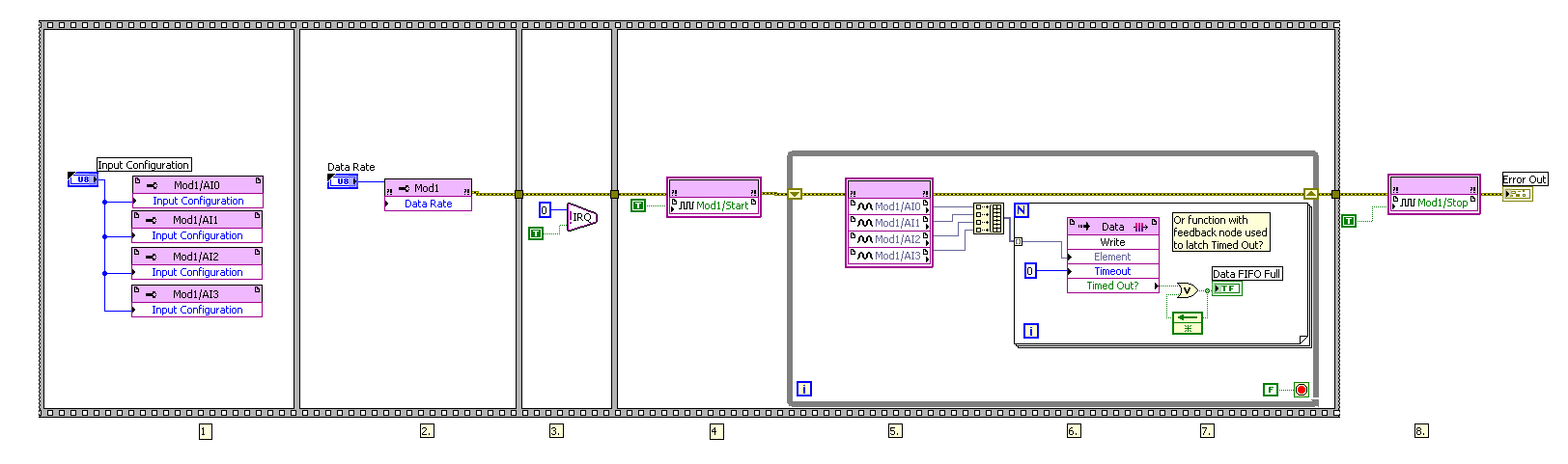
I try to write data from a host of RT on target FPGA using DMA FIFO and then process these data and read then return of the FPGA target to the host of the CR through an another DMA FIFO. I'm working on the NI SMU chassis 1062 q, with the built-in NI SMU-8130 RT controller and target FPGA NI SMU-7965R.
The problem I face is that I want to send three different tables, two of the same size and the third with different size, and I need one more small to be sent first to the FPGA. I tried to use encode dish with two executives in the FPGA VI. In the first image, I read and write the first table in a while loop which is finite (that is, a finite number of iterations). The second frame contains the process of reading and writing the second two tables (of the same size) in a while loop that can be finite or infinite (depending on a control). The problem is that it does not work. 2 arrays are displayed on the front panel of the RT VI host and works well, however, the table that should have been read in the first sequence does not appear on the front panel of the RT VI host. It is not sensible because if it is not passed from the host to the fpga and vice versa then the second image should not have been executed. Note that I'm wiring (-1) for the time-out period to block the while loop iterations until the passage of each item is completed. So the first while loop has only 3 iterations. Could someone help me undersdtand why this happens and how to fix this?
I enclose a picture of the host and the fpga vi.
Thank you.
If you vote for my idea here and it is implemented, you can even omit the loop FOR fully.

(I also propose the RE / IM divided inside the loop FOR and perform operations on complex table before the loop the transpose and reshape .) In this way, you only need one instance of these operations. You might even save some unnecessary allocations table in this way)
-
Reading of the zeros of a DMA FIFO empty
Hello
I'm having a problem using the DMA FIFO to communicate between my real-time system and my FPGA. I use two DMA FIFO, one-way to the FPGA of the RT system and then vice versa. I can successfully get data to and from each system; However, before, after and sometimes inbetween my data, I'll get a seemingly random assortment of zeros. In the latest version of my code (which I have provided) I read the number of items stored in the DMA FIFO and read only this number to my RT system to try to get the data that I want and no zeros, but this does not work either.
I'm new to both in real-time and FPGA and so it certainly feels like I'm missing something very basic. I tried dealing with this problem by myself well and have had absolutely no success and would appreciate any help.
My equipment includes:
A Dell laptop (used as a host of the user interface)
1082 chassis
Controller of 8133 (running the LabView RT operating system)
7965R FPGA
5781 module for FPGA (not currently in use)LabView 2014 SP1
On the side of RT, you need to use a structure of the case so that you have not read of the FIFO if no data is available.
I would also like to change the flow of network to be inside of your time in a loop until the user interface capturing each data point, as it comes (connect before the loop, close after the loop and write it as the data come from the inside of the loop). This will save memory (which is VERY important in a RT system) since you don't have to set up the table.
You write only as an element in the FPGA. So any sous-suite readings should give you an array of 0 s, causing 0s back upward. You must maintain the Timed Out in the FPGA so that the data will only until to the RT when there is real data to send. Your FPGA code could be reduced to this:

-
Number of DMA FIFO of items to read mismatch in the FPGA and RT
Hi all
I use myRIO, LV14 to run my application.
Request: I have to continuously acquire data via FPGA and host RT process once every 2000 samples are taken. I use DMA FIFO (size 8191) to acquire data, use timeout property in the FPGA to eliminate the buffer overflow. I had followed cRIOdevguide to implement this part. An excerpt of what I put in place is attached. All code runs in the SCTL at 50 MHz.
Question: Two or three times I met with this strange behavior, the FPGA FIFO gives continous timeout and the RT is unable to read the FIFO. The number of elements to set the property in the FPGA VI gives 0 showing that FIFO is full and no more can be written, but the RT, remaining items gives 0, so it is reading 0 (none) elements.
Solution: I put a case where I'll write to FIFO (under the code) and if the number of elements to write is different from zero. It seems to work fine, from now.
What confuses me, is that my FPGA VI said that FIFO is full (number of items to write 0 = FIFO) and gives a timeout error, but RT VI said that number of items remaining in the FIFO is 0 and therefore no data is read. No idea why this is so? My RT and FPGA VIs continues to run, but with no gains or to read data.
A few minutes after you run the code, I've seen this behavior. No idea why this happens? I try to reproduce the behavior, and will update if I meet with her again. Sorry, I can't post my code here, but I guess the code snippets to explain some extend.
Thank you
Arya
Edit: Even with the mentioned workaround solution, the problem persists, now that the FPGA written any of FIFO. And the RT VI is not able to read all the elements he sees 0 items in the FIFO. The FIFO continues to be in a State of timeout. So I guess that the problem is on the side of RT.
Why it looks like you read from the FIFO even in two different places in the same VI, at the same time? If the lower reading throws the FIFO, it will never trigger the reset, which could lead to the situation you describe, I think (it's hard to tell from a few screenshots).
Also, your logic seems too complicated. I immediately noticed that there is no reason to select the entry, the output of = 0 - simply use the 'equal to zero' output directly. On the side of FPGA, why you need check the number of items that you want to write? There's nothing wrong with writing in a FIFO that is already full. just the data won't get written.
-
Two DMA FIFO fill and asynchronous playback?
Hello
I work lately on the Labview for my system which includes the acquisition of data from two sensors in FPGA vi and communicate to RT vi, where I treat the two sensor data and subtract. I am facing a problem of synchronization. I tried 4 data points, 2 of each sensor to each 25th microsec. Here I attach a pseudo-code that is just one of my original code that shows the same problem.
When we run the code, acquire US 4 data points each 25 microsecs in the FPGA vi and storing in the fifo DMA 2.
Then, I read this in RT vi and display them.
When I have a single loop in the FPGA and RT vi. the number of elements left in the two fifo should be identical, I perceive.
But in this case, it is not. Please enlighten me why?
Concerning

Intaris is right. How work DMA FIFO is that they fill a small pad on the FPGA, and when this buffer is almost full, the data is copied (automatically and at the bottom) of a larger buffer in the memory of the host. The remaining items is the amount of data is left in the buffer of the host. The automatic copy of the FPGA to the host will happen precisely at the same time to the two FIFOs, so you will get different amounts of data in each. The total number of items (between the pads FPGA and host) should be the same, although there is no way to see that, except for read all data (until the two buffers are empty) and confirm that the total number of items of reading was the same.
-
Reading and arraya thro DMA FIFO (PCI7813R)
Normal 0 21 false false false SL X-NONE X-NONE MicrosoftInternetExplorer4 / * Style Definitions * / table. MsoNormalTable {mso-style-name : « Navadna tabela » ; mso-tstyle-rowband-taille : 0 ; mso-tstyle-colband-taille : 0 ; mso-style-noshow:yes ; mso-style-priorité : 99 ; mso-style-qformat:yes ; mso-style-parent : » « ;" mso-rembourrage-alt : 0 cm 5.4pt cm 0 5.4pt ; mso-para-marge-haut : 0 cm ; mso-para-marge-droit : 0 cm ; mso-para-marge-bas : 10.0pt ; mso-para-marge-gauche : 0 cm ; ligne-hauteur : 115 % ; mso-pagination : widow-orphelin ; police-taille : 11.0pt ; famille de police : « Calibri », « sans-serif » ; mso-ascii-font-family : Calibri ; mso-ascii-theme-font : minor-latin ; mso-hansi-font-family : Calibri ; mso-hansi-theme-font : minor-latin ;}
Hello
Location:
I read 5-position encoder with PCI7813R. The position of encoder data format is I32. Following is each position encoder converted to U32 and build in a table by using "build the array function. Finally this table guided loop where I write it in DMA FIFO uses "FIFO write function. FIFO depth is equal to 16383 and Timeout to 0.
Side host I'm reading this table of DMA FIFO. The host FIFO depth is set to 1000000. I use 'Method Invoke with FIFO read' to read data from the FIFO. I read 10000 elements each time. Data output is converted to I32 and guided an extension to "decimate the 1 d array function. I use 5 indicators to represent the positions of Encoder on the host side.
And now the problem:
Position 1 Encoder shell displayed on indicator 1. But every time I close my application and run it again this position appears on the other indicator. Sometimes is the position of the Encoder 1 shown on the 1, sometimes on the indicator 5 indicator, sometimes on indicator 3... Although this position of the encoder is shown every time on the other indicator it has correct values. What I'll do as I will always receive encoder position 1 on indicator 1, position of the Encoder 2 Indicator 2...
My application has been built according to these instructions:
http://zone.NI.com/DevZone/CDA/tut/p/ID/4534
TNX,
Gregor
Normal 0 21 false false false SL X-NONE X-NONE / * Style Definitions * / table. MsoNormalTable {mso-style-name : « Navadna tabela » ; mso-tstyle-rowband-taille : 0 ; mso-tstyle-colband-taille : 0 ; mso-style-noshow:yes ; mso-style-priorité : 99 ; mso-style-qformat:yes ; mso-style-parent : » « ;" mso-rembourrage-alt : 0 cm 5.4pt cm 0 5.4pt ; mso-para-marge-haut : 0 cm ; mso-para-marge-droit : 0 cm ; mso-para-marge-bas : 10.0pt ; mso-para-marge-gauche : 0 cm ; ligne-hauteur : 115 % ; mso-pagination : widow-orphelin ; police-taille : 11.0pt ; famille de police : « Calibri », « sans-serif » ; mso-ascii-font-family : Calibri ; mso-ascii-theme-font : minor-latin ; mso-hansi-font-family : Calibri ; mso-hansi-theme-font : minor-latin ;}
Sorry Jochen, I placed the function reset at the end of my routine. L I corrected (put it on the beginning of the routine) and now it works as it is supposed to be.
Thanks a lot again!
Kind regards
Gregor
-
How to choose the maximum number of items for DMA FIFO to the R series FPGA
Greetings!
I'm working on a project with card PCIe-7842R-R series FPGA of NOR. I use to achieve the fast data transfer target-to-host DMA FIFO. And to minimize overhead costs, I would make the size of the FIFO as large as possible. According to the manual, 7842R a 1728 KB (216KO) integrated block of RAM, 108 000 I16 FIFOs items available in theory (1 728 000 / 16). However the FPGA had compilation error when I asked this amount of items. I checked the manual and searched online but could not find the reason. Can someone please explain? And in general, what is the maximum size of the FIFO given the size of the block of RAM?
Thank you!
Hey iron_curtain,
You are right that the movement of large blocks of data can lead to a more efficient use of the bus, but it certainly isn't the most important factor here. Assuming of course that the FIFO on the FPGA is large enough to avoid overflowing, I expect the dominant factor to the size of reading on the host. In general, larger and reads as follows on the host drive to improve throughput, up to the speed of the bus. This is because as FIFO. Read is a relatively expensive operation software, so it is advantageous to fewer calls for the same amount of data.
Note that your call to the FIFO. Read the largest host buffer should be. Depending on your application, you may be several times larger than the size of reading. You can set the size of the buffer with the FIFO. Configure the node.
http://zone.NI.com/reference/en-XX/help/371599H-01/lvfpgaconcepts/fpga_dma_how_it_works/ explains the different buffers involved. It is important to note that the DMA engine moves data asynchronously read/write on the host nodes and FPGAs.
Let me know if you have any questions about all of this.
Sebastian
-
Target to host DMA FIFO not compensation when they are arrested
I use a PXI-7841R (Virtex5) and 32-bit data to the host via DMA FIFO transfer. When you read the FIFO on the host for the first time, the data are "stale" (which means that it is not what is currently coming in the FPGA, but what came in a few seconds ago stale). I tried both a stop and a configuration for clear memory FIFO before I use them. Documentation on one or both of these so-called clears the target and host the FIFOs. Does not help in both cases. With readings of the second and the following, FIFO has then 'valid' (same data as it appears on the FPGA entry node). What is curious is that each reading exactly the same thing:
- Stop the FIFO (must erase all data)
- Elements of reading 375 of the FIFO. (repeated playback of the FIFO)
Also interesting: FPGA FIFO is implemented for 255 elements. The first 255 items host-side contain the data "stale" on the first reading. It reminds me of the never erased FPGA FIFO.
Answered by support OR. The documentation for the FIFO, stop and configure FIFO is in error. Cars of documentation will be written against them.
Solution:
These methods remove only the FIFO on the side host. Data FPGA FIFO must be read following until no element.
-
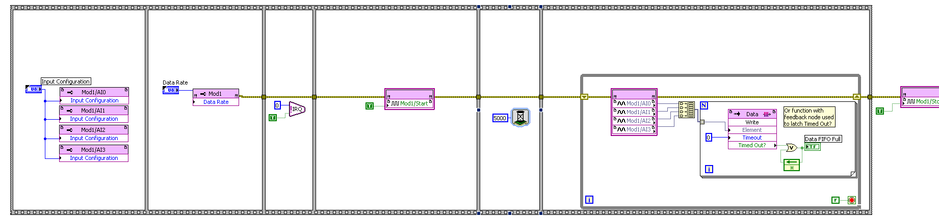
DMA FIFO of FPGA to host RT is full
I transfer data via DMA FIFO of FPGA to host RT.
DMA FIFO is full, I have tried everything I know:
-increases the size of the FIFO DMA up sideways FPGA
-set the depth of the FIFO DMA to 100000000
-increases the amount of DMA FIFO reading in each iteration of the loop
-use a timed with a frequency of 1 MHz, instead of a normal life all loop
Please find attached my project folder, FPGA code and code RT.
I solved my problem.
Below you will find my FPGA code before solving the problem and after resolution of the problem.
Solution: I just added a function of 5000 milliseconds (5 seconds) to wait before getting the analog input nodes samples (AI).
Before:
After:
-
simple DMA FIFO reading two analog channels
Hello
I have a question on a method of data transfer between two analog inputs for a simple DMA FIFO in FPGA. The code is described here: http://decibel.ni.com/content/docs/DOC-6303. If I use this method, and I got out in a graph of my host VI, the calendar in the graph reflects the same schedule as the signals that have been entered? Or will they be phase shift between two signals?
Thank you
Grant
Grant:
Because it is not all information of timing with the signals in the FIFO, there will be no lag phase on the chart.
Hope that helps. I would like to know if I forgot something, or who does not explain very well.
Thank you!
-
Hello
I have the next vi FPGA and RT vi (joint). I'm trying to transfer data from the FPGA to the RT vi (using the target to host DMA FIFO), then to plot the data in the RT vi. The signal that I take analog input also is a 10 Hz, 1 well module 9215 V sinusoidal amplitude.
However, in the RT vi, I get only one exit fluctuating, with only the values 0 or 1. Also I see no time-out that happens with the RT parameters vi as: 'TimeOut = - 1' and "Count (uC) = 25".
Why would this be happaning?
Thanks in advance...
Mandar-
Hi Mandar,
Not with 8.6. You told me 8.5 documentation (I didn't know you were using this version). Take a look at the following article; It should solve the problem that you are facing:
How can I transfer my data to fixed-point using a FIFO in LabVIEW?
-
What would be the effect of the adjustment of the depth of DMA FIFO before every read?
I'm using a PXI-7813R FPGA board using a 3rd party API. I had a few problems during playback. I looked in their API (LabVIEW) code and realized that they were in DMA FIFO depth before each reading of the FIFO. This apparently does not cause a failure of catastrphic issues I have observed are only transitional in nature.
What kind of problems, if everything can these operations cause or will be ignored because the FIFO is already running?
Thank you...
mgerceker,
According to the help file , that should be OK to do even though I could see it being a problem if it is not set correctly before performing an operation. What kind of symptoms do you observe?
Greetings from Austin,
-
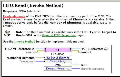
Read DMA FIFO: reads + deletes?
Just to double check:
An invoke for read DMA FIFO method: reads and deletes the oldest elements of the FPGA FIFO?
I mean that it removes after reading? Porbaly deletes.
It is not mentioned in the documentation of expelicitly:
Yes, reading is destructive (meaning that it removes the element of the FIFO).
-
How is managed using DMA FIFO (target host) host matrix
Hi people,
I'm trying to pass an array of values of the host to the FPGA using DMA FIFO. Let's say 20000 items in the table. My FIFO host side can contain only 16000 items or almost. The data will be written element by element regardless of the size of the table or do I need to partition the table in small paintings before writing the FIFO method? Let's say that I write for the FIFO with berries small, 1000-element. The FIFO will read 1 element both of the side FPGA so the stream is blocked until I have at least 1000 free items on the FIFO method write, how he writes every 1000 the next setpoint at the same time? Or target values will be written permanently as soon as the individual elements are erased by the number of available items to write?
Hi Nathan,
Sorry for the late update, but I just thought that I should follow. I followed your advice and try it tested just for me (I probably should I have done it before posting). Turns out that the data table will write even if there is not enough empty elements to contain the table in its entirety. However, it always crashes until enough information is read and erased from memory on the side FPGA for the whole table. So if it's data that are constantly being played, it's always better transmitting data through in the form of smaller tables if you do not want to increase the amount of memory FIFO host OCCUPIES on your system. However, if you can afford the memory while you mentioned, you can always increase the depth of the FIFO on the host side. As I understand it, try to write more big berries to a host to target FIFO buffer does not diminish overhead costs (as is the case with a target to host FIFO) as it still passes an element at a time to the FIFO of FPGA-side without worrying.
Thanks again for your help.
Kind regards
John has
Maybe you are looking for
-
Satellite A200 - 26 d: black screen when I try to play the video in full screen
Hello I hope someone can help, when trying to play a video full screen on my laptop I get only audio and a black screen - can anyone help? Thank you very much Fiona
-
I would like to enlarge the text in the toolbar firefox 6.0.2. (file, edit, view, etc.)
The Firefox toolbar is rather small and sometimes hard to read depending on the circumstances. I would like to expand the toolbar and text to double its current size. How then?
-
Problem with Wifi on all Apple devices on my network
Hello everyone, a few days ago, I started having WIFI problems on my network at home with only the APPLE DEVICES, we have a MacBook Pro 2012, two IPhone 6 + s and also a PC all WIFI windows running on a Netgear R7000 Nighthawk (ISP Comcast). The wind
-
I just spent 2 days and $100 by working with a company whose seat is in India to fix my computer. First issue was wireless printing. I have HP PHotosmart Plus, and it has been printing for 4 months. Then it would not print anything either from the
-
the control panel fixed association, he say of cereate Association for this
PPS. I can not open emails with attached pps more. He said, to create an association in THE SET ASSOCIATION CONTROL PANEL