DMA FIFO of FPGA compilation error
Hello
I have a cRIO 9074 with FPGA. I tried a simple piece of code to learn how to acquire the data that is generated on the FPGA at a rate of 10 KHz and transfer it to the host VI to treat later in offline mode. However, I meet this compilation error when you compile the FPGA VI base containing a node to write FIFO (photo of the VI attached below). In compiling the report, it is said that there are 256 RAM Block used (the total number is 40), so an error has occurred. The error notification of exact compilation from Xilinx report is reproduced below:
# From the PAM program
# o toplevel_gen_map.ncd - intstyle xflow-calendar toplevel_gen.ngd map
toplevel_gen. FCP
#----------------------------------------------#
"Target part using" 3s2000fg456-4 ".
Design of mapping in the lut...
Guided running of packaging...
Running based on the delay of packaging of LUT...
ERROR ack:2310 - type compositions "RAMB16" too found to adapt to this device.
ERROR: card: 115 - the design is too large to fit the device. Please consult the Design summary section to see what resource requirements for your design exceeds the resources available in the device. Note that the number of slices don't notice it that their packaging could not be completed accurately.
NOTE: A file NCD will be always generated to allow you to examine the mapped design. This file is intended for evaluation use only and will not be processed successfully by means of BY.
Mapping performed.
See the report of map file "toplevel_gen_map.mrp" for more details.
Problem encountered during the packaging phase.
Summary of design
--------------
Error number: 2
Number of warnings: 125
ERROR: Xflow - card program returned the error 2 code. Aborting the workflow execution...
Bitstream not created
Time history analysis
What does that mean? How can I fix this error?
Thank you
Bogdan
Hey,.
Have you already tried to reduce the size of the FIFO memory?
Christian
Tags: NI Software
Similar Questions
-
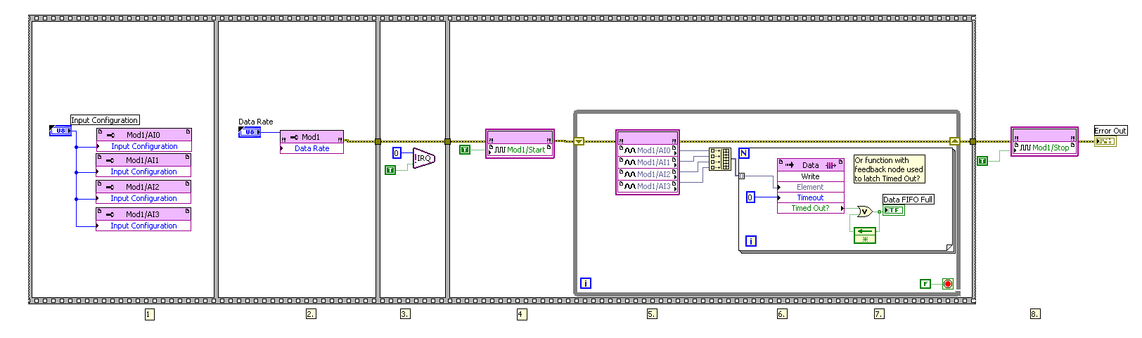
DMA FIFO of FPGA to host RT is full
I transfer data via DMA FIFO of FPGA to host RT.
DMA FIFO is full, I have tried everything I know:
-increases the size of the FIFO DMA up sideways FPGA
-set the depth of the FIFO DMA to 100000000
-increases the amount of DMA FIFO reading in each iteration of the loop
-use a timed with a frequency of 1 MHz, instead of a normal life all loop
Please find attached my project folder, FPGA code and code RT.
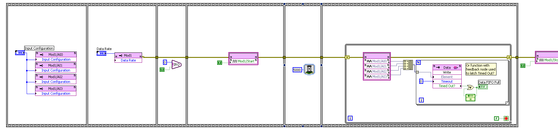
I solved my problem.
Below you will find my FPGA code before solving the problem and after resolution of the problem.
Solution: I just added a function of 5000 milliseconds (5 seconds) to wait before getting the analog input nodes samples (AI).
Before:
After:
-
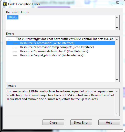
A Labview program with 4 DMA FIFO on FPGA card that can support DMA only 3
Hello
I am a beginner on LabVIEW FPGA, my internship that I work on the previous intern program, there during his internship and he published this program in its report.
On his program, it's that he put 4 DMA FIFO, but supported the FPGA (PXI of NOR-7951) map where we work me and the trainee takes only 3 DMA, so I can't run the program, I have this error:
I wonder if it's a bug or anything else, any ideas?
Sorry to answer the longer end, thank you for your response thank you for your help I could change my program, now the program run with three 3 DMA, I used a table to 2 signals in a single FIFO DMA.
I show the program, that can help someone with the same problem.
-
tables of fixed size in FPGA compilation error - how to implement a waveform control in an FPGA?
Hello
After being stuck for two days, please let me briefly describe my project and the problem:
I want to use the cRIO FPGA for iterative control of waveforms. I want to capture a full period of the waveform, subtracting a reference waveform period and apply control algorithms on this. Subsequently the new period of correction must be sent again for the output module OR. If it does not work, the captured waveform will look like the one reference after several iterations.
I am planing to create an array of size fixed for the capture and the reference waveform (each around 2,000 items for a given period). I use so 2 paintings of each elements of 2000. I use the function 'replace the subset of table' to update each element captured in the loop sampling and a feedback for each table node to keep in memory (I also tried shift registers, but then the berries do not have a fixed size any more and I can't start the compilation process).
If I try to compile the FPGA vi, I get the following error:
Details:
ERROR ortability:3 - Xilinx this application runs out of memory or met a memory conflict. Use of current memory is 4167696 KB. You can try to increase physical or virtual memory of your system. If you are using a Win32 system, you can increase your application from 2 GB to 3 GB memory using the 3 G switch in your boot.ini file. For more information, please visit Xilinx answer Record #14932. For technical support on this issue, you can open a WebCase with this project attached to http://www.xilinx.com/support.
"Synthesize - XST" process failedBefore I added berries to my code I could compile the FPGA without problems. So, it seems that the tables are too big for the FPGA. :-(
Therefore, I would like to ask if there is perhaps a better method to implement my problem in LabVIEW FPGA? How could avoid the tables to save my waveforms on a period?
Thanks a lot for your help in advance.
Best regards
Andreas
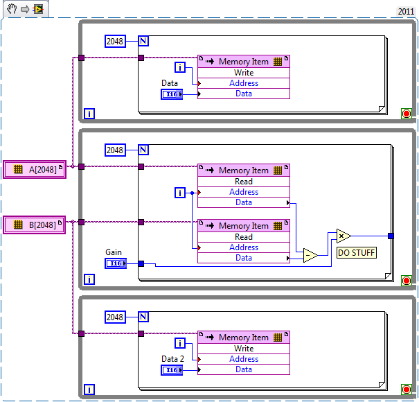
Unfortunately, the LabVIEW FPGA compiler cannot deduct stores shipped from berries (yet). When you create these two large paintings, you are creating essentially several registers very, very large. Just by looking at your picture, I guess that there are at least 4 copies of each of the tables.
You want to use LabVIEW FPGA memories instead. You can create memories outside the loop and then read/write them where you are currently referencing the berries. The only change that you really need to do is to break down your treatment in scalar operations. I have attached a simplified version of your plan, I hope it helps. Let us know if you have any other questions.
-
I'm converting a piece of code from 8.5 to 2011. When I tried to compile the fpga vi to a bit file, I get the error attached. Why is this? Thank you!
The thing is that the only solution that I found about this error is to install a patch or repair/reinstall Xilinx or LabVIEW FPGA tools.
Christian
-
FPGA compilation error sbRIO 9632
Hi guys,.
I'm trying to write a simple piece of code to send a PWM signal to a PIN on my sbRIO-9632 (starter kit 2.0) to order a servo. I used the example of 'control a servo using PWM' and my code is pretty much the same. When I try to generate/compile the FPGA VI, it stops after only 4 to 6 minutes, saying an error has occurred. The compilation appears to hang during the process of the "card".
The example is for a sbRIO-9631 so I created a new project for my robot Robotics and changed the PIN e/s that I use (Port5/DIO9). I search through forums but cannot find a solution to this :/
I have attached my code and the XilinxLog file with it.
Thanks for any help!
MortZ
Hello
Sorry for the late reply! Have you made progress?
Unfortunately, your zip file seems to be disabled on my PC. How it has been compressed?
So what I meant by remove the digital Pulse.vi to generate, is to see if it affected the compilation. Please see if you can compile the FPGA code with the following approach:
Create the new project > add your target sbRIO > add the VI attached to this post to your FPGA target > compile
I think it would be beneficial to you to see if the problem is the compilation itself or the code you are trying to compile.
In addition, you have any another available PC? Might be a good idea to see if your code compiles on another PC.
Please make sure you have LabVIEW Real-time and LabVIEW FPGA installed (it should come with the Robotics module, but I recommend that you check that they have indeed been included).
If the build process fails to map no matter what you do, I propose the following: make sure that the target passes a self-test of MAX. reinstall the Xilinx tools (only if it seems that the issue is not with the code, but with the compilation process itself).
Good luck

Best regards
Christopher
-
cRIO 9014, FPGA compiler error
I use cRIO 9014, that while the FPGA code compilation I get attached error.
Please guide me ob who...
Hi Olivier,.
The displayed error is clear.
Your system time is older than the time of installation.
Change to correct time and try it...
In addition, if you change your system time (IE computer), some software will not work. (another example is Gmail. Try to connect to Gmail after year settting in the previous year in your system. It displays error SSL.).
-
Hello
can someone tell me how to stop Fifos DMA as a target host on the level of FPGA FIFO?
The node of the method 'stop Fifo' host only erases the fifo buffer on the host side. The Fpga FIFO is still running.
To reset the whole fpga is not possible, because the running code is important for control of the measure.
Thank you very much
Hi b.,.
you might stop to write in the FIFO with a Boolean control connected to a structure of matter...
-
Transfer 1 d table using DMA FIFO of FPGA
I'm transferring a table 1 d of two U32, with a configured U32 FIFO for the host.
but I get the error because of the connection to different types of terminals,
It seems very simple, I found a lot of samples with a very similar treatment here, but I don't see the problem?
There is a loop of indexation of array... The write operation is therefore the element by element.
The operation of reading (on the host) can read several items at once (--> a table).
-
FPGA Compile Error - Xilinx error
I am compiling my FPGA VI on my laptop and have failed to do. The VI compiles correctly on my PC lab. I tried to uninstall and reinstall LabVIEW FPGA and Xilinx tools without change.
I'm running SP1 2014.
I've attached my log for compiling file. I tried to geenrate a new specification to build with no change. Compilation of a white VI works fine.
The FPGA VI has some registers and interacts with the DIO card using FPGA.
I appreciate all help.
Matthew
So, I finally determined what was the problem.
I had created a junction of Windows for several directories for some files out of a second disc of port. As regards to Windows is, C:\NIFPGA is exactly and is supposed to hide the fact that he is really D:\NIFPGA.
Well, apparently, he does not hide that quite some programs. I noticed in the Xilinx log file that it maintained exchange between C:\NIFPGA and D:\NIFPGA. So, I tried a Windows symbolic link to Diretcory, which is similar to the junction (according to my research, the junction is supposed to be the 'best'), and now it seems to work correctly.
So the lesson here is: If you want to move this directory NIFPGA, reinstall the system, or use a symbolic link to remap the directory, not a junction.
-
simple DMA FIFO reading two analog channels
Hello
I have a question on a method of data transfer between two analog inputs for a simple DMA FIFO in FPGA. The code is described here: http://decibel.ni.com/content/docs/DOC-6303. If I use this method, and I got out in a graph of my host VI, the calendar in the graph reflects the same schedule as the signals that have been entered? Or will they be phase shift between two signals?
Thank you
Grant
Grant:
Because it is not all information of timing with the signals in the FIFO, there will be no lag phase on the chart.
Hope that helps. I would like to know if I forgot something, or who does not explain very well.
Thank you!
-
For a DMA FIFO running from the host to the 7976 is a data type that is optimum for PEP?
For transmission to the host 7976, I can pack my data in say U64s or break up in U8s. Y at - it a data type that will give the best rate? Maybe based on the bus (SMU) or the implementation of RIO drivers behind the scenes?
My experience is different. Once, I did a load of tests with different widths DMA FIFO for FPGA and tested the throughput and latency. If sending data via U8, U16 or U32 DMAs, I saw the same total transfer of bps. My explanation for this? Given that the width of the DMA is 32 - bit, LV little packaging in order to ensure that each part of the 32 bits is used. This means that if you have a DMA U8, it will transfer at a time, 4 to DMA 2 both U16 or U32 DMA one at a time. 64-bit is divided into two individual transfers.
Do not use FXP. Even a 1-bit FXP is represented internally as 64-bit and will require TWO DMA transfers to an FPGA.
Side fromt hat, U8, U16 or U32 makes essentially no difference because they are all packed 32-bit internally.
-
How to choose the maximum number of items for DMA FIFO to the R series FPGA
Greetings!
I'm working on a project with card PCIe-7842R-R series FPGA of NOR. I use to achieve the fast data transfer target-to-host DMA FIFO. And to minimize overhead costs, I would make the size of the FIFO as large as possible. According to the manual, 7842R a 1728 KB (216KO) integrated block of RAM, 108 000 I16 FIFOs items available in theory (1 728 000 / 16). However the FPGA had compilation error when I asked this amount of items. I checked the manual and searched online but could not find the reason. Can someone please explain? And in general, what is the maximum size of the FIFO given the size of the block of RAM?
Thank you!
Hey iron_curtain,
You are right that the movement of large blocks of data can lead to a more efficient use of the bus, but it certainly isn't the most important factor here. Assuming of course that the FIFO on the FPGA is large enough to avoid overflowing, I expect the dominant factor to the size of reading on the host. In general, larger and reads as follows on the host drive to improve throughput, up to the speed of the bus. This is because as FIFO. Read is a relatively expensive operation software, so it is advantageous to fewer calls for the same amount of data.
Note that your call to the FIFO. Read the largest host buffer should be. Depending on your application, you may be several times larger than the size of reading. You can set the size of the buffer with the FIFO. Configure the node.
http://zone.NI.com/reference/en-XX/help/371599H-01/lvfpgaconcepts/fpga_dma_how_it_works/ explains the different buffers involved. It is important to note that the DMA engine moves data asynchronously read/write on the host nodes and FPGAs.
Let me know if you have any questions about all of this.
Sebastian
-
Number of DMA FIFO of items to read mismatch in the FPGA and RT
Hi all
I use myRIO, LV14 to run my application.
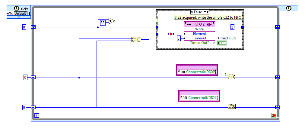
Request: I have to continuously acquire data via FPGA and host RT process once every 2000 samples are taken. I use DMA FIFO (size 8191) to acquire data, use timeout property in the FPGA to eliminate the buffer overflow. I had followed cRIOdevguide to implement this part. An excerpt of what I put in place is attached. All code runs in the SCTL at 50 MHz.
Question: Two or three times I met with this strange behavior, the FPGA FIFO gives continous timeout and the RT is unable to read the FIFO. The number of elements to set the property in the FPGA VI gives 0 showing that FIFO is full and no more can be written, but the RT, remaining items gives 0, so it is reading 0 (none) elements.
Solution: I put a case where I'll write to FIFO (under the code) and if the number of elements to write is different from zero. It seems to work fine, from now.
What confuses me, is that my FPGA VI said that FIFO is full (number of items to write 0 = FIFO) and gives a timeout error, but RT VI said that number of items remaining in the FIFO is 0 and therefore no data is read. No idea why this is so? My RT and FPGA VIs continues to run, but with no gains or to read data.
A few minutes after you run the code, I've seen this behavior. No idea why this happens? I try to reproduce the behavior, and will update if I meet with her again. Sorry, I can't post my code here, but I guess the code snippets to explain some extend.
Thank you
Arya
Edit: Even with the mentioned workaround solution, the problem persists, now that the FPGA written any of FIFO. And the RT VI is not able to read all the elements he sees 0 items in the FIFO. The FIFO continues to be in a State of timeout. So I guess that the problem is on the side of RT.
Why it looks like you read from the FIFO even in two different places in the same VI, at the same time? If the lower reading throws the FIFO, it will never trigger the reset, which could lead to the situation you describe, I think (it's hard to tell from a few screenshots).
Also, your logic seems too complicated. I immediately noticed that there is no reason to select the entry, the output of = 0 - simply use the 'equal to zero' output directly. On the side of FPGA, why you need check the number of items that you want to write? There's nothing wrong with writing in a FIFO that is already full. just the data won't get written.
-
Transmission of data to the host of RT to the FPGA via DMA FIFO
Hello
I try to write data from a host of RT on target FPGA using DMA FIFO and then process these data and read then return of the FPGA target to the host of the CR through an another DMA FIFO. I'm working on the NI SMU chassis 1062 q, with the built-in NI SMU-8130 RT controller and target FPGA NI SMU-7965R.
The problem I face is that I want to send three different tables, two of the same size and the third with different size, and I need one more small to be sent first to the FPGA. I tried to use encode dish with two executives in the FPGA VI. In the first image, I read and write the first table in a while loop which is finite (that is, a finite number of iterations). The second frame contains the process of reading and writing the second two tables (of the same size) in a while loop that can be finite or infinite (depending on a control). The problem is that it does not work. 2 arrays are displayed on the front panel of the RT VI host and works well, however, the table that should have been read in the first sequence does not appear on the front panel of the RT VI host. It is not sensible because if it is not passed from the host to the fpga and vice versa then the second image should not have been executed. Note that I'm wiring (-1) for the time-out period to block the while loop iterations until the passage of each item is completed. So the first while loop has only 3 iterations. Could someone help me undersdtand why this happens and how to fix this?
I enclose a picture of the host and the fpga vi.
Thank you.
If you vote for my idea here and it is implemented, you can even omit the loop FOR fully.

(I also propose the RE / IM divided inside the loop FOR and perform operations on complex table before the loop the transpose and reshape .) In this way, you only need one instance of these operations. You might even save some unnecessary allocations table in this way)
Maybe you are looking for
-
Can I retrieve my text Messages from my apple account
Can I retrieve my text Messages from my apple account
-
Can I connect two monitors to a PC Tower? cc = us
Can I connect two monitors to a PC Tower?
-
When I click on the item to taskbar Windows 7 to Firefox (or on the Start Menu, too), he asks me each time if I really want to open this file: ... \ick Launch\User Pinned\TaskBar\Mozilla Firefox.lnk I say YES and it opens... until next time, when he
-
What is the difference between asus enrich your life and enrich your life rt
I'm not sure
-
How can you communicate with Adobe?
Hopw you contact Adobe?