Failure of compilation of the FPGA target
Hi all
I met a problem when I tried to compile my target FPGA VI. Failed to compile for some reason any to halfway after start of the compilation. I post a few screen shots of the labview error information.
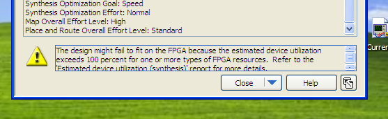
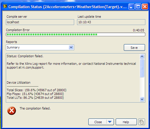
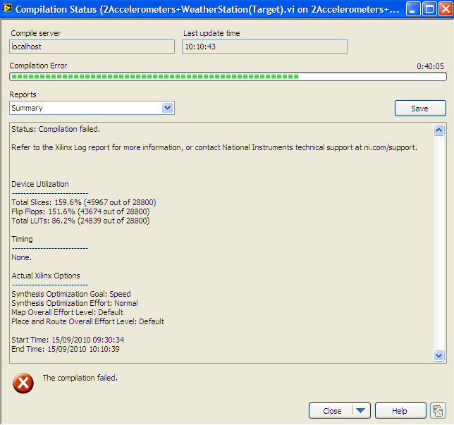
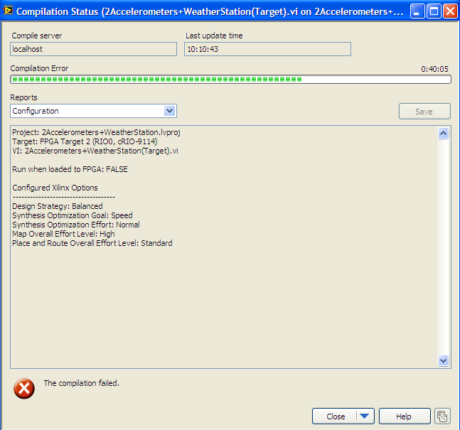
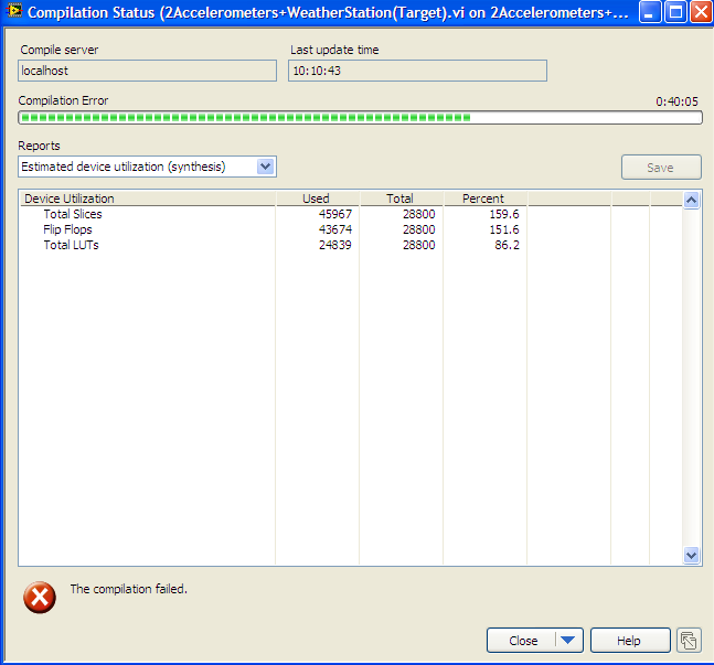
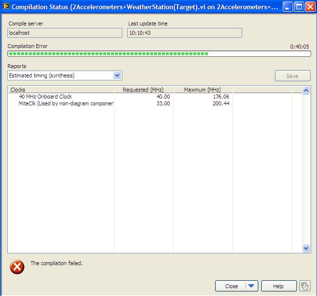
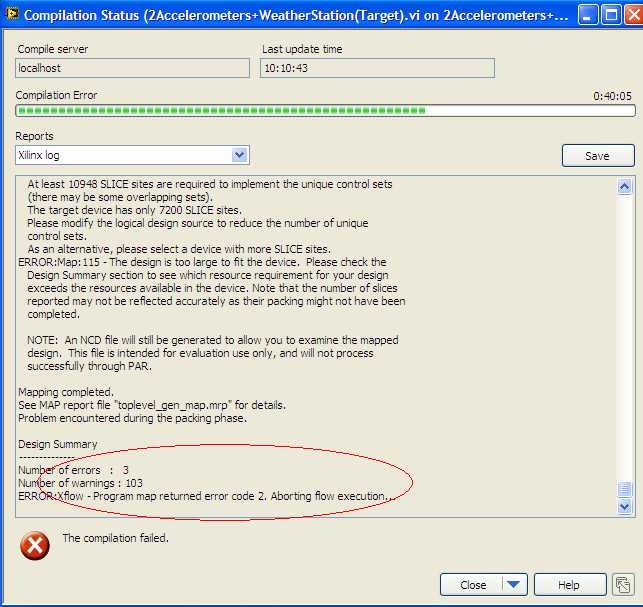
What causes this problem? How could I solve this problem?
Thank you very much!
Kind regards
masterwho
Also you have large networks on the Panel before the FPGA VI?
Or is there the great paintings inside the code?
If you can, put a piece of your code.
Tags: NI Software
Similar Questions
-
Error: Execution of registry is supported only on the FPGA target
I am trying to write a debugging tool to test the communication between objects FP on my host VI to a RT system and then to a FPGA system. I thought I would "simulate" the three layers with queues between them in order to ensure that the parameters are received correctly - a comprehensive test of Communications virtually. I want to be able to run this VI on the host. There are a lot of bits being shifted and twisted and be able to define probes and braekpoints within a single host VI is an advantage.
Initially, it worked fine after copying my FPGA code (with object instantiation of the registers and then reading and writing for them), but now then LabVIEW did another thing that disappears (with no goodbye or anything like that). When I say that it worked, the values read from the FPGA objects that instantiate their own records showed the correct values when sending data. This means that LV really instantiate records and has been able to address them individually.
Since then, I get the error appearing in the title, whenever I try to run the VI.
(1) should I really move my parts FPGA to a VI on the FPGA target and have the VI in parallel with the defined target to run in Dev mode (and sends data over the DMA channel)
(2) why this work initially and then fail?
Shane
False alarm, I had no wired all my objects instantiated (and thus a communication VI received default objects with no valid registry.
Program actually works very well.
Still weird, but the error message doesn't really leave everything that was wrong.
Shane.
-
Xilinx FPGA target properties options is not available
Hi all... I have a little problem.
I can't have Options of Xilinx FPGA target properties to change the goal of optimization of the synthesis of area instead of the speed in 2012 of LabVIEW. Please let me know the cause and the solution to this problem.
Thank you.
Coelho,
Interesting, looking to the right place for the compiler options? Compiler options will not be under 'Properties of the FPGA target' as you mentioned previously (sorry I missed this in your first post), rather these options can be found under the heading 'Options of Xilinx' when you create a specification to build FPGA for compilation.
"" Click on build specifications ' New ' Compilation, and then select the Options of Xilinx category and you should see a window like this.
Can you confirm that you are looking at this place?
-
Areas of clock in the FPGA examples
I was looking through some examples of LabVIEW FPGA and I fell on the example of Crossing Clock domains.
In this example, there are 4 screws; FIFOs.vi; Global Variables.vi; Local variables.VI; and Registers.vi. In each of these screws, there is a timed loop which runs at 160 MHz.
How is that possible? Since the clock on the FPGA is only 40 MHz. did I miss something?
On the FPGA target, you can right click on the clock of 40 MHz and create a derived clock which can be a multiple where for a fraction of the base clock (40 MHz).
160 MHz is a trivial example of 4 times the base clock.
-
Transmission of data to the host of RT to the FPGA via DMA FIFO
Hello
I try to write data from a host of RT on target FPGA using DMA FIFO and then process these data and read then return of the FPGA target to the host of the CR through an another DMA FIFO. I'm working on the NI SMU chassis 1062 q, with the built-in NI SMU-8130 RT controller and target FPGA NI SMU-7965R.
The problem I face is that I want to send three different tables, two of the same size and the third with different size, and I need one more small to be sent first to the FPGA. I tried to use encode dish with two executives in the FPGA VI. In the first image, I read and write the first table in a while loop which is finite (that is, a finite number of iterations). The second frame contains the process of reading and writing the second two tables (of the same size) in a while loop that can be finite or infinite (depending on a control). The problem is that it does not work. 2 arrays are displayed on the front panel of the RT VI host and works well, however, the table that should have been read in the first sequence does not appear on the front panel of the RT VI host. It is not sensible because if it is not passed from the host to the fpga and vice versa then the second image should not have been executed. Note that I'm wiring (-1) for the time-out period to block the while loop iterations until the passage of each item is completed. So the first while loop has only 3 iterations. Could someone help me undersdtand why this happens and how to fix this?
I enclose a picture of the host and the fpga vi.
Thank you.
If you vote for my idea here and it is implemented, you can even omit the loop FOR fully.

(I also propose the RE / IM divided inside the loop FOR and perform operations on complex table before the loop the transpose and reshape .) In this way, you only need one instance of these operations. You might even save some unnecessary allocations table in this way)
-
Tests of changes in the fpga without reloading code
I understand that after a fpga code is changed, it must be recharged in the fpga. Is there a way to test the code fpga on PC without reloading the file bit in the fpga every time? Thank you!
Yes - with the right button on the FPGA target in the project and choose "run VI on...» "You can always run in simulated simulation with IO. Some devices take care of simulation with real IO so. Of course it won't work not anywhere near the actual speed, but you can use the standard LabVIEW tools such as probes, highlighting the execution and debugging breakpoints.
-
Cannot deploy when you use the FPGA configuration file
Hi all
I'm new to NI Veristand. We use a controller NIPXI 8108 with a map of FPGA OR 7841R. Is the used chassis OR PXI 1042 q. VeriStand does not deploy, when we try to add the target FPGA. For adding, we used the default for NOR 7841R provided with veristand FPGA configuration file. The error is attached! Without adding the FPGA target, we are able to deploy.
We programmed with LabVIEW FPGA card and it works.
Please help us!
Thank you
SID
Hi Sid
This is because the FPGA card is not connected through the chassis
Right click on the (unidentified) PXI system and identify as PXI 1042 q.
Right-click on the PXI-1042 q system and identify the PXI-8108 controller.
Then it will automatically fill the devices under the controller
Now try to deploy again. It will work
-SID
-
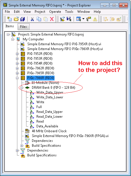
How to add a FIFO 128-bit DRAM to the FPGA project?
How can I add the DRAM FIFO - 128-bit memory Interface to an SMU-796XR RIO module?
Above project is examples of projects. I know how to add DRAM but not how to set as FIFO 128 bits as shown above.
Any guidance is appreciated.
Right-click on the FPGA target-> properties
Select Properties DRAM on the left side of the Popup.
Change the mode of the two shores to CLIP nested LabVIEW FPGA memories.
Click OK.
The project will be auto-updated with new DRAM memory, it will be empty.
Right-click on the DRAM-> properties
Enable
Select FIFO 128 bits
-
ERROR: TclTasksC:process_077: in the FPGA Compilation
Hi all
I use for my application in which I am facing following error when compiling my fpga code compact rio 9072:
Compilation failed due to an error of Xilinx.
Details:
ERROR: TclTasksC rocess_077: did not finish. Please, look in the newspaper and report files.false
When running
"process run"card.
(file "C:\NIFPGA\jobs\XI64xG6_My449tj\map.tcl" line 6)ERROR
ack:2310 - type compositions "SLICEL" too found to adapt to this device.
ERRORack:18 - the design is too large for the device and package.
Please see the Design summary section to see the cost estimates for
your design exceeds the resources available in the device.
NOTE: A file NCD will be always generated to allow you to examine the mapped
Design. This file is intended for assessment use only and will not be processed
successfully through NOMINAL.
This NCD mapped file can be used to assess how the logic of the design has been
mapped in FPGA logic resources. It can also be used to analyze
preliminary to the level logic (route pre) calendar with one of the static electricity of Xilinx
analysis of synchronization (PRHT or Timing Analyzer) tools.
Summary of the design:
Error number: 2
Number of warnings: 69
Use of logic:
Number of slice Flip Flops: 7 886 on 15 360 51%
Number of 4-input lut: 16 104 on 15 360 104% (OVERMAPPED)
Distribution of logic:
Number of slots occupied: 8 744 7 680 113% (OVERMAPPED)
Number of slices only related logical container: 8 744 100% 8 744
Number of slices that contains no logical relationship: 0 to 8 744 0%
* See NOTES below for an explanation of the effects of unrelated logic.
Total number of 4 input lut: 17 400 on 15 360 113% (OVERMAPPED)
Number used as logic: 15 998
Number used as a middle way: 1 296
Number used as Rams 16 x 1: 82
Used number recorded the shift: 24
The logical Distribution report slice is not significant if the design is
too mapped to a resource not slices or if Placement fails.
Number of IOBs servile: 183 on 333 54%
BIO flip flops: 74
Number of RAMB16s: 1 24 4%
Number of MULT18X18s: 2 on 24 8%
Number of BUFGMUXs: 4 to 8 50%
Number of DCMs: 1 on 4 25%
Fanout of the Non-horloge nets on average: 3.38
Peak Memory use: 361 MB
Total in time REAL in the completion of the card: 1 dry 12 mins
Time CPU until the end of the total map: 1 dry 12 mins
NOTES:
Related logic is defined as logical that share connectivity - for example two
Lut are "related" if they share common inputs. During Assembly of the slices.
Card gives priority to combine the logic that is related. Generates so
best performance of synchronization.
Without logical report does share no connectivity. Card will start only packing
logic not related in a slice once that 99% of the slices are held through
logical packaging partners.
Note that once the logical distribution reaches the level of 99% by related
logical packaging, this does not mean the device is completely used.
No logical report package will begin, continuing until all usable LUTs
and FFs are busy. According to your timing budget, an increase in the concentrations of
logical packaging unrelated can adversely affect the performance of timing set
your design.
Mapping performed.
See the report of map file "toplevel_gen_map.mrp" for more details.
Problem encountered during the packaging phase.
Failure of the process 'Map '.Start time: 18:29:23
End time: 18:44:42
Total time: 00:15:19Can someone tell me why this error came?
Thank you best regards &,.
Vipin Ahuja
Vipin Hello,
It seems that your code requires more resources that are available on the FPGA. Optimizing your code can help to solve your problem:
You may have noticed some "Overmapping", mentioned in the newspaper:
Number of 4-input lut: 16 104 on 15 360 104% (OVERMAPPED)
Distribution of logic:
Number of slots occupied: 8 744 7 680 113% (OVERMAPPED)Take a look at this article:
http://digital.NI.com/public.nsf/allkb/060BA89FE3A0119E48256E850048FFFE?OpenDocument
And this:
http://digital.NI.com/public.nsf/WebSearch/311C18E2D635FA338625714700664816?OpenDocument
Kind regards
Navjodh
National Instruments
-
Run code on the host target RT and FPGA
Hi all
I'm sorry if I ask a question to repeat. I searched for this a bit and couldn't find a solution.
I'm trying to run a single VI (be it on RT compactRIO or on the connected host PC) and enforce the code on the host PC and target the FPGA code RT. I currently code that runs on the host PC computer that opens the FPGA reference and executes code FPGA, but I don't know how to do this with a VI on the target of RT. Any advice/help would be great. Thank you!
Brandon
You are not far from your goal. But you need to at least
- Update FPGA code (Bitfile) containing your code to run on the FPGA.
- An executable compiled for your goal of RT, which is set to autostart.
You can use the code from my first post as a starting point. Compile, deploy and set it to autostart on your target of RT. - An executable compiled for the host machine. that your user will begin.
You can use the code in my first post, maybe load IP address, Port etc. of the Ini file settings.
If you double-click on the exe file on your host computer it will open an application reference to your target computer of RT and call the VI on the target machine. This is how you run code on your RT. From this RT code you can download and run the FPGA (bitfile) to your FPGA code or control which is already running the FPGA by controlling a state machine code. Load more screws to your memory of RT targets and call them from your host to add more functionality if you need to.
-
FPGA target 9146 OR editions variable defined by the user to a network
I am developing code to use on the expansion chassis NI 9146 ethernet with 3 hanging modules, NI 9205, NI 9264 and NI 9476.
The code is supposed to be downloaded on the chassis as FPGA code and run the code itself and the release of information on the network for the chassis, it is hanging in. The code is simple (blood pressure measurement and convert them to pressure).
When the code is on the host pc, it can be run through the target and runs correctly. The pieces are just have thing chassis user FPGA 1 LED blink a few times per second, convert the voltage in pressure and variable output on the network and read some Boolean variables that are on the network. All variables are not listed in the network in this way (by pressing the button run an FPGA VI compiled host) by pressing
When the FPGA VI is downloaded to the flash memory chassis, configured to run once downloaded and restarting the device, the VI FPGA runs, because user FPGA 1 LED flashes on the specifided rate in the code, but variables do not put on the network.
Attached are several screenshots of the code window and screen project.
Thank you for your time
Mitchell
Hello
The FPGA cannot write to the variables by itself. It is usually used to make a task of high speed. In order to communicate with a host computer, you will need the code running on the controller that uses screws FPGA Interface.
-
compilation process 'Map' FPGA failure failed
Hi all
We bought a new cRIO 9068 and I try to get installed it in a new project with some new maps. We have also improved our projects to LV2013 - sp1. I was unable to complete a compilation of the bitfile FPGA. It takes place during 25 minutes and when it will do the "Utilization, (map) of final device" it fails. Looks like I might be missing something, I have, but I have installed and reinstalled LV2013 and versions of Xilinx (10.1 and 13.4 or 14.4) which does not seem to solve the problem.
Any ideas on what he seeks can be as useful as a search on 'Map' did not help.
Thanks in advance.
I found the solution. There are additional items on the WAY lead the FPGA Compiler for the installation of VS I have instead of the executable 'Map' that she needed. I removed the path to the VC\include directory and now it compiles. Probably screwed my VS, but that's another day.
-
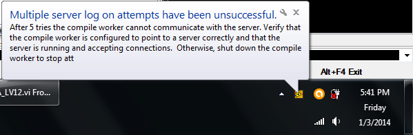
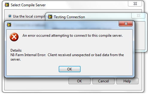
Internal error OR-farm - impossible to compile the FPGA VI
Hello!
When I try to compile any FPGA VI with LabVIEW2013 or 2012 SP1, I get the following error:
"Year error occurred trying to connect to this server compilation."
Details:
Internal error OR the farm: Client Server received unexpected or bad data. »
Intermediate files are not generated, the error message appears immediately after I have select build of build specification or I click the run arrow.
I use the local server for compilation.
The equipment I use: CompactRIO Evaluation Board - SbRIO9636, DELL laptop, Intel core2 Duo T5800, 2 GHz, 3 GB RAM, Windows 7 Ultimate 64-bit, SP1.
The intermediate files CAN be generated without any problems if I select in the menu. If I run the FPGA application compile worker, a ToolTip message specifying that "FPGA compile runs", but after a few seconds, another message appears: newspaper several attempts were unsuccessful - please see attached images.
At first, I thought that my firewall (Comodo 6.3) is the reason for this, so I disabled it but nothing changed. Then I tried to fix LabVIEW FPGA and XILINX tools with the firewall disabled but din do not solve the problem. I tried with LabVIEW SP1 of 2012 and 2013.
If you have any suggestions, please let me know! Thank you!
We would like that you try to reset the NIAuth database by following these steps:
1. go to Windows Services (Bring up Windows with Ctrl + Alt + Delete Task Manager, click the Services tab, click the Services button at the bottom right of the window.
2 stop the NI Application Web Server and NI System Web Server services in this order (right click, stopping service and select).
2 backup, and then delete all the files under %PROGRAMDATA%\National Instruments\NIAuth: registry.bin and commitmark.
3. run NI System Web Server and NI Application Web Server services in this order.
4. navigate to http://localhost:3580 / connection of an IE on the local computer and try to log in with username "admin" and password empty. Succeeds, the server will return one signed in as: message from the admin.
After you follow these steps, try and connect to the FPGA compiler, and then let me know what are the results.
-
Disable the extended FIFO FPGA target during execution
Hello
I use a FIFO extended target in my FPGA to constantly calculate the derivative of a measured value (dB/dt). Thus the FIFO stores all values during time dt. This means dt determines the number of items in the FIFO and dB is determined by the actual value less the oldest value in the FIFO. It works well when I initialize with the code in figure InitFIFO.
But the FIFO of compensation is not possible (see figure clearFIFO). In the while loop if "reset dB" is false, as the new value of B is written on the FIFO, then the oldest value is read from, for the number of items in the FIFO remain constant. To change dt during execution, I need to clear the FIFO and initialize it with a new length (number of items). I tried the next loop, but it does not work. The FIFO does not initilized with the elements. The length is zero and the loop counter for (#deltaB Length2) is 0.
What I am doing wrong? Is there a better way to erase a FIFO during execution in the FPGA? I'm now stuck for 2 days with this problem and looking forward to any idea or suggestion.
Thank you very much. Best regards
Andy
Hej,
Thank you for your response. You were correct, that deltab FIFO length was 0 because the defalt value was zero. The problem is that in my host vi on the RT system I put DeltaB FIFO length in a loop of high priority and as you can see when I restart the FPGA, DeltaB FIFO length has a valid value (the code in figure 1 works well with a local variable of DeltaB FIFO length in the FPGA). But the variable to set the variable "reset dB" is under the control of the loop of low priority of the host vi. And there, I had an entry DeltaB FIFO length unwired.
So, I learned that a control FPGA read/write unwired sends a '0' or resets the variable to its default value in the FPGA. I assumed that nothing is transferred and the last variable is retained if you let a control read/write unwired. Now, I learned of this stupid error!
Thanks a lot again!
Andy
-
Compilation of the variable results in LabVIEW FPGA
Hello. I would ask why LabVIEW FPGA generates different results of compilation for the same code. When I compile several times my code, the maximum speed and total changes bitfile slices generated according to the compilation, but I does not alter with the FPGA VI. In addition, is the precise relationship of compilation? Thank you
It's normal. The FPGA compiler starts to place pieces of code on the FPGA somewhat randomly and adjusts them until either the design adapts and responds to the criteria of the moment or there that the compiler determines that it cannot fit all the code and meet time constraints. The outputs that the FPGA VI generates when run will always be the same.
Maybe you are looking for
-
How can I download my Thunderbird AddressBook on my computer?
I want to download my address book in Thunderbird on my computer. Is this possible? Thanks for any help you can give.
-
Satellite A665-S6054: backlight keyboard and Fn + z accessibility
Hey guys I came across a problem which then lead to another Firstly I have updates have been made to my computer but only recently have noticed that the Fn + z does not control my backlit keyboard more Seeing that all the other functions (that I know
-
Lenovo y50-70 extremely boring stutter LAG!
So I've only had this laptop for a week already and I look forward to all of its features, except that I experience extreme stuttering gal. The stutter lag effects games, software, etc... The shift goes something like this: Hello you are t-t-t-t-t-t-
-
VIsta... user profile service didn't login. Failed to load profile
Attempted to restart... Press f8... not going than to sign... f12... even... get impossible to spend here to do a system restore...
-
IPS sensor - Event Notification by e-mail?
Good day to all. I was asked to recreate some features after he lost the customer improved VMS to the CSM but without CS-MARCH or any other event monitor. The user has had the system to generate an email when an event was triggered. He was apparently