FPGA and digital i/o Modules
Hi all
We have NI 9421 digital input and digital output NI 9472 Modules. We can run these modules into a VI under the 9073 cRIO chassis. While we have added the FPGA target under the same chassis, we cannot use the modules. We also install the scan engine.
How can we use FPGAS and i/o Modules at the same time?
Once you add a target FPGA in CompactRIO chassis, when you deploy the code, the cRIO is configured for the FPGA mode, which requires a bitfile compiled to connect with the C Series modules. Remove the target FPGA or changing the mode of chassis in the project and by redeploying must reconfigure the cRIO for scan Mode, which allows you to use the IO module directly from the RT VI.
For more information, see this post.
Tags: NI Software
Similar Questions
-
LabVIEW FPGA and real-time communication module
Hi all
I created a small program in labview FPGA which gets continually distance from the HC - SR04 ultrasonic sensor. The rest of the robot program is written in the time module real Labview. Is it possible that the distance calculated by FPGA module to read in time real module.
I used the FPGA just because there micro-deuxieme counter, which helps me get the distance from the ultrasonic sensor.
Thanks in advance.
There are many ways this can be done, according to your needs.
See the help article transfer of data between the FPGA and host (Module FPGA) for a breakdown of each method.
-
sbRIO-9631 digital inputs/outputs using e/s node FPGAS and FPGA of i/o method node
Hello, I'm trying to configure my SBRio-9631 for the first time. I try to use the on boards to inputs and digital outputs. The following code will work? This is a simple "read the entries, 'or' some inputs and pass ' exits." I have to add "E/s method nodes FPGA" between my 'FPGA of i/o nodes"to get"modes of State of sorting for the input and output lines? Also, I can't simulate/test it works, by adding 5 VDC at the entrances, and not have any source of voltage output. Thank you for your time.
Hey, Spex,.
I really, really appreciate your help. Your follow up information was exceptional.
Thanks again for your help and your time.
gjmm
-
What is the use of FPGAS and how it differs from the IO Modules
Hi all
Maybe it's a silly question for most of you. But I have very less knowledge about the basic concepts of electronic (FPGA, real-time) to cRIOs. I know that FPGA
can be used to generate circuits within the chip that helps by some logical functions.
I've just started working in the cRIO. My question is that we have Modules e/s making it outputs all the application entry. So, what is the purpose of e/s in the FPGA.
Lets consider that we entered for an application of RTD. In this case the module NI 9217 itself exits 24 bits of data from the RTD measurement which may be the process of the LabVIEW VI. What will be this FPGA between the i/o Modules and the processor will help in? Also I want to know what type of communication is used to send data between the FPGA and host modules.
Thanks in advance
Ajay HI:
Sorry, you do not have an answer to your original question. However, you are right about the benefits of the FPGA. You said, if you build pre-processing in the FPGA, you can unload a lot of potentially CPU calculations out of the host processor. In addition, the program running on the FPGA is highly deterministic and can run the code very quickly. So if you build a kind of guard or evanescent dog part of your application, the FPGA is a good place to put it.
To answer your other questions, communication between the modules and the FPGA is generally above the SPI and the data can be transferred between the FPGA and host via DMA FIFO operating on the PCI bus or single point save access using read/write in the FPGA host Interface controls. You can also use interruptions in signal of disputes between the FPGA host.
I hope this helps, but let us know if you have any other questions.
-
Resources on Rio fpga using the NI 9403 module
I use a CRIO and it works very well with my A/D and D.-a. When I add an e/s digital NI 9403 module, it eats all my resources even if I don't use all that in the circuit! Is there a way where I can use say only 2 or 3 pins e/s and not other use without him swallow all my resources.
I found the problem. When I added the module e/s I used the mode of discovery and he went. It seems it went past Scan mode for some reason any. When I moved the unit on Solution Explorer up next to two other files, I had made A/D D - A mode FPGA, he changed his mode of FPGA itself and then I could remove I/O pins as required. The icon, then changed when I pulled a PIN on my FPGA block diagram and everything was ok.
-
How to use the target FPGA and co. on the same chassis cRIO?
I have a cRIO system consisting of a master chassis 9074 with several modules IO and EtherCAT 9144 slave unit.
I want to run a CIE (see: http://zone.ni.com/devzone/cda/epd/p/id/5333) on the chassis of the master, this uses the analytical engine. At the same time I have to do some very urgent measures if I want to use the Board in hybrid mode, using analysis and FPGA engine at the same time (as described here: http://digital.ni.com/public.nsf/allkb/0DB7FEF37C26AF85862575C400531690.)
But as soon as I add the FPGA target at one of the chassis, the feature of the ice on this chassis stops working. After some research, I found that the CIE can initialize is no longer the modules belonging to the frame that has the target FPGA on it. Error in the method Init of the CIE is: 65700 (indeterminate). This occurs when you try to use "for a more specific class' on the modules configured with a target FPGA on it.
Someone knows what can cause exactly this problem and perhaps provide a solution/work around?
Many thanks in advance.
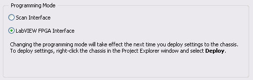
Hybrid mode requires you to have a bitfile compiled running on the FPGA to be able to read the Scan Interface IO Variables. Move the target FPGA at the RT target module will allow Interface of scanning for this module, but the frame will always mode Interface of LabVIEW FPGA.
To get fair access to the scan mode for the frame, right click on the chassis in the project, and choose Properties. Then, modify the Scan Interface programming. If you want to continue using the programming of FPGA and the Scan Interface set (hybrid mode), you will need to compile a bitfile (empty if you do not want programs on the FPGA again or containing your FPGA code). By compiling, the support of the module scan mode for the modules under your RT chassis is compiled in your custom bitfile. Then, on your VI RT, you need to use reference FPGA VI open to your newly compiled VI. Once this VI is deployed and ongoing implementation, you get the data from you are the CIE.
For more information, see this knowledge base article and Reference Interface of Scan CompactRIO and procedures.
-
Fortunately the cRIO merger two time real screws: analog and digital output
Howdy,
I need help with a cRIO code. The purpose of the code is to acquire an analog input from the NI 9234 c series module and be able to send a "signal of pulse" digital camera (first low for some time, t1, then high for some time, t2) from a NI9401. Separately, I wrote the code to perform both tasks. However, when I add the code of RT digital output pulse pulses to analog input RT code, the DMA FIFO overflows because of the way that my digital pulse output code works. Currently, there are two reasons which overflows of the FIFO:
- The digital output code is pending for a while loop (pending "Send Pulse" become a true), the loop I can't empty the buffer FIFO
- The FIFO is not enough, quickly emptied depending on how long the pulse (t1 and t2) times are. The way I keep the pin high or low for a defined period of time is by issuing a sleep command, which blocks the loop I empty the FIFO. (Is there a "best" way to sleep?)
I have attached photos of my codes FPGA and RT. Please give me a suggestion on how to marry my two loops of RT for the use of happy resources! Thank you.
I found a quick way to solve this problem. I moved the timing of the Digital pulse on the FPGA. So whenever I have a Boolean value, the FPGA generates a waveform with the settings I put (a pulse in my case). This works because the FPGA loops run in parallel, I think. That's why, when I run a pending order in the loop of FPGA digital output, it does not prevent the FPGA of analog input loop to run. I have attached a picture of the code.
-
Producer consumer with inputs and outputs analog and digital
Hello world
I'm working on a program of control system for some practical test work. Currently, I am working on the data acquisition of the Labview program component. My architecture is consumer-product loops with a what. My system will have analog inputs, outputs, analog inputs and digital outputs. It is not a criticism of time sytem, but I wish that all the acquisition of data to synchronize. I enclose my program because it is at the moment. I have difficulties to get all the data in the since that I have two types of data. In addition, I don't know if I have synced the four sequences of read/write correctly. I would be very happy if someone could take a look at my program and give me some advice. Thanks in advance.
-
analog and digital data synchronization
Hi all
I would like to help with what I seek to accomplish, if you don't mind much.
I'm trying to synchronize the acquisition of analog and digital modes using a common trigger that launches both types of data collection at the same time. What I've done so far, is wasting his time trying different combinations to gather examples of LabVIEW 2011 on the synchronization of data - namely the 'Multi-multifunction-Synch AI lu Dig Chan.vi' and 'Multi-Device Synch-Analog Input-Finite Acq-Analog Start.vi.
I tried to combine the two, because one contains digital and analog, the other contains the trigger for multiple tasks.
I guess I should place the trigger (either digital or analog-eventually I will want to choose) then call the "Get Terminal name with device Prefix.vi. But from there I'm not sure wheter to connect the name of the terminal of the sample clock digital channel or a digital leading edge of the digital chain trigger.
Also, the way it is wired now I get errors at the local terminal name, so I don't know exactly where this terminal must come from.
I try my best, I could use a little help, I have attached my attempt with the examples that I speak to you.
Thank you.
Hi beefcake.
The CtrInternalOutput internal output line is used as sample for your digital output sample clock source clock. If you change the settings for your CO Pulse Time is Dev1 and your digital output is Dev2, you will notice that the name of the product terminal would give Dev2/CtrInternalOutput. So what you get here, it's as well as the digital output device sees his sample clock, instead of the clock itself.
If you just want to use a digital/analog input as your trigger, you should do something more as in the example above. Do you use multiple devices, or are all your lines on the same device? This example is more complicated because it is synchronization of signals on several devices.
Looking at how this VI is wired, you can see that the digital signal triggers the analog signal. You want the analogue signal must be started first, so that when the digital signal triggers the analog task is already running and can trigger immediately. If the digital task started first, it can trigger until the similar task had started, and they do not exactly trigger at the same time.
I hope that clarifies things. Kind regards
-
Analog acquisition and digital simultaneous DAQmx
Hi all
I use the USB-6212 acquisition card to acquire analog and digital inputs. However, I encountered some problems that I don't know how to solve.
All channels (analog and digital input) is independent of one another, but should be acquired at the same time (using the same clock, I think), but I'm not managing to achieve; In addition, I can not put a task so that the digital acquisition is made by "continuous sample" - the error says it is not supported, but I saw this configuration in other examples in this forum.
The only way to get a digital waveform must keep pooling the entry? And, therefore, also in common analog input? Is it not this costly approach from the point of view resources?
Best regards
The decrease of performance will be determined by the speed of your computer and your USB hub.
I think that to get the hardware timing of digital I/o on a USB device, you're going to have to step up to a card in the X series as the 6341, but I'm not sure about this. You can find this specification under the specifications of each product tab. Looking for 'Material' under DIO > Timing.
-
How to trigger and outputs analog and digital Outout tasks begins on a counter to start?
Hello
I'm trying to synchronize the start of a task outputs analog, a task of digital output and a task of counter. I want to start the counter to serve the master trigger and analog and digital tasks to synchronize his departure.
I guess I need something like:
analogOutputTask.Triggers.StartTrigger.ConfigureDigitalEdgeTrigger ("?", DigitalEdgeStartTriggerEdge.Rising);
digitalOutputTask.Triggers.StartTrigger.ConfigureDigitalEdgeTrigger ("?", DigitalEdgeStartTriggerEdge.Rising);
analogOutputTask.Start (); Slave 1
digitalOutputTask.Start (); slave 2
() counterTask.Start; n / / master
Where? is a string specifying a command source for the beginning of the task of the meter. However, I can't find what this string. Any suggestions?
Thank you!
-Jon
Just FYI, the solution to this problem as well as some other ones is encapsulated in a short example .NET, I created. It is on the Web site of EITHER:
http://decibel.NI.com/content/docs/doc-15500
This project shows how to synchronize all your analogue/digital outputs through tasks and forums in terms of synchronizing Calendar and start clock.
-Jon
-
Number of DMA FIFO of items to read mismatch in the FPGA and RT
Hi all
I use myRIO, LV14 to run my application.
Request: I have to continuously acquire data via FPGA and host RT process once every 2000 samples are taken. I use DMA FIFO (size 8191) to acquire data, use timeout property in the FPGA to eliminate the buffer overflow. I had followed cRIOdevguide to implement this part. An excerpt of what I put in place is attached. All code runs in the SCTL at 50 MHz.
Question: Two or three times I met with this strange behavior, the FPGA FIFO gives continous timeout and the RT is unable to read the FIFO. The number of elements to set the property in the FPGA VI gives 0 showing that FIFO is full and no more can be written, but the RT, remaining items gives 0, so it is reading 0 (none) elements.
Solution: I put a case where I'll write to FIFO (under the code) and if the number of elements to write is different from zero. It seems to work fine, from now.
What confuses me, is that my FPGA VI said that FIFO is full (number of items to write 0 = FIFO) and gives a timeout error, but RT VI said that number of items remaining in the FIFO is 0 and therefore no data is read. No idea why this is so? My RT and FPGA VIs continues to run, but with no gains or to read data.
A few minutes after you run the code, I've seen this behavior. No idea why this happens? I try to reproduce the behavior, and will update if I meet with her again. Sorry, I can't post my code here, but I guess the code snippets to explain some extend.
Thank you
Arya
Edit: Even with the mentioned workaround solution, the problem persists, now that the FPGA written any of FIFO. And the RT VI is not able to read all the elements he sees 0 items in the FIFO. The FIFO continues to be in a State of timeout. So I guess that the problem is on the side of RT.
Why it looks like you read from the FIFO even in two different places in the same VI, at the same time? If the lower reading throws the FIFO, it will never trigger the reset, which could lead to the situation you describe, I think (it's hard to tell from a few screenshots).
Also, your logic seems too complicated. I immediately noticed that there is no reason to select the entry, the output of = 0 - simply use the 'equal to zero' output directly. On the side of FPGA, why you need check the number of items that you want to write? There's nothing wrong with writing in a FIFO that is already full. just the data won't get written.
-
Card FPGA and data acquisition synchronization
Hi, we are control and data acquisition of several hardware devices (including Photodetectors and translational stages). Until last week, we used all the controls and acquisition using a PCIe-7852R FPGA board. However, we decided to move the acquisition part to a PCIe 6363 DAQ card to improve the sharpness of the tension. During the test, I found that the internal clocks in the FPGA and the DAQ cards are slightly inconsistent (not just a phase delay, but a difference in the period).
I know because I have generated a square wave (period = 20) using the FPGA and gains using the data acquisition card (at a rate of 200 kHz, that is, 1 taste every 5). I have observed acquired place shifts 5 every 5 seconds approximately. Such a change does not occur if the production and acquisition is done using the same Board. Therefore, the only explanation is that the data acquisition and FPGA cards clock frequencies are different. According to my calculations, the percentage difference between their time clock must be 5/5 s = 0.0001%.
Therefore, I wonder if there is anyway to synchronize clocks between them. Or, is it possible that I can drive the FPGA clock-based DAQ hardware, or vice versa? Also, please let me know if there is something trivial as I fix.
Thank you very much.
Kind regards
Varun
Hi Varun,
my post was only one solution...
Your data acquisition card may take an entry to control sampling of trigger. In this mode, samples draw on a rising edge of the external clock signal. As long as you stay within the limits of the DAQ (100 MHz for your card) material sampling works perfectly. There are even examples coming with LabVIEW explaining how to program your data acquisition card...
This mode use you your FPGA as clock source sampling for data acquisition. Both will run on the FPGA clock in sync. When the FPGA is a bit out of 40 MHz, so it won't matter because both devices are triggered on the same clock signal...
-
What are the differences between LabVIEW and LabVIEW FPGA and LabVIEW RT
I need a comparison of LabVIEW, LabVIEW FPGA, and LabVIEW RT
Sorry, I misunderstood.
LabVIEW RT (LabVIEW Real-time) combines graphical LabVIEW of programming with the power of a real-time operating system, allowing you to create applications in real time.
-
NEITHER USB-6343 analog and digital grounds
In the manual for the NI USB-6343, it is said that the mass input/output, analog and digital terrestrial are related, but by a small sign. For my application, I am attaching all 3 these grounds to exit the box (I'm tie all areas with physical threads). It is perhaps a silly question, but it's OK to do, correct?
This should be OK unless there are large currents flowing on ground conductors. If you have important currents in the ground, you have other problems that must be resolved before you connect the DAQ hardware.
Lynn
Maybe you are looking for
-
IPhone crashed the Middle updated and now stuck on the setting of the screen!
My Iphone has been unusually slow. So I tried to update my phone I thought it's maybe the old version of the IOS that makes my phone lag (I think I downloaded the latest version, 10. something). While trying to update my phone, it crashed at halfway.
-
Cannot use iTunes on the iMac to sync apps for iPhone
I can relocate (from the screen to the other), install, and remove icons on my iPad via iTunes. I use the left side of the screen "App" for that section. However, I can't do it all on my iPhone 6. In addition, the IOS app icon is now absent on iPhone
-
Player and Media center stop working
How to remove the program and reinstall
-
My hp printer photosmart c4750 is available for eprint
Got what I want to use on my iPad 2
-
Cannot find download for CS4 Design Standard
Hello worldI bought a copy of CS4 Design Standard a few years ago and still use it today. I update my 2009 MacBook to a MacBook Pro 2012 which is not a disk drive so I need a download of this edition. When you look at the list of downloads I don't se