FPGA resources
When I look at my compilation report for my code FPGA on a PXI-7833R. I see the settings below. They are all listed separately. However, I thougth a slice consists of the register and LUT, isn't it? Records of slice and Slice LUTs explain just more Total slices? If so, I don't see how the calculation works in my attached compilation report.
Total slices
Records of slice
Slice LUTs
Block RAMs
jyang72211 wrote:
The total range is therefore to what I'm looking for in terms of capacity, right? Let's say I
Total installment: 100%
Slice the registry: 60%
Slice LUTs: 60%
I must conclude that my FPGA is full, even if a few slices are not entirely uttialized. There is no way to make the FPGA using these partial slices, right?
No, still not quite right. The compiler FPGA constantly optimize once all adapts and responds to the timing (or it determines that there is no possible way so that everything fit). If you add more logic to your design, the compiler may be able to do all this in shape, although the compilation will take more time.
Even more confusion, if you're just on the edge of what you can adapt, sometimes the compilation will succeed and other times, it will fail for exactly the same code, because the compiler (really the place-and-route step) uses a random starting point to place the logic.
For a very simplified analogy, let's say you have a collection of triangles (registers) and squares (LUT) that you want to stay inside a piece of paper. If you have only a small number of triangles and squares, you can put them anywhere. The numbers are rising, you must arrange to pack them more closely, and when it starts to get very tight, you may have to try several times to make it all be adapted. That's what makes the FPGA compiler, with additional restrictions on where the logic can be placed due to delays.
Tags: NI Software
Similar Questions
-
Reverse and pseudo inverse Matrix on FPGA
Hi all
How can I calculate matrix inverse/pinv on pushed more logical clock (*.gcdl), for FPGA? (Labview Comms 2.0)
Maybe someone has a solution for this task? Or that the best algorithm I use for this task?Thank you.
Hello togoto,.
We have matrix Inverse and matrix screw Pseudo-inverse for code side host, but these are not supported on FPGA. The reason for this is because without a known matrix size, there is not a way to implement a dynamic matrix math function (the compiler couldn't know how many resources which requires). If we consider that more algorithms of inverse depend on the division, which is very intensive on FPGA resources, which provides another reason why we would be unable to put implementation in CDL.
That being said, Comms has Matrix multiply and transpose the matrix of features that you can implement in CDL. Because for a long time the matrices are always a fixed size and uniform, you can implement a custom algorithm to achieve pseudoinversion and matrix inversion. It would take careful pipelining to ensure it worked in a single clock cycle.
Could you elaborate on what exactly the application is supposed to accomplish? If possible, the math movement matrix your screw host-side may be the best approach.
Best,
Daniel
-
Violation of FPGA Timing-> how to find?
Hello
I encountered a problem of violation of timing during my FPGA code compilation. Even if I change the options of compilation for "balanced" or anything else, the problem is still there.
My question now is, how do I find the function block in my code where the problem occurs? I use the SCTL several in my code.
Thanks in advance
Use the controls for the FPGA-host communications as long as you have enough of FPGA resources. It is recommended to use the communication between the host and FPGA DMA FIFO.
Only controls on the higher-level FPGA vi are accessible on the side of the host.
Global variables are used to communicate with an FPGA scope exclusively.
You use a device of sbRIO so I think the FPGA to communicate with the aim of RT (host)...
-
use of devices high cRIO 9068 FPGA
Hello. I have problems with my cRIO 9068 (dual-core, Artix 7 667 MHz), which uses a lot of FPGA resources. I did a little VI FPGA (LabVIEW 2013 SP1) allowing USER FPGA led to two colors (green and orange) for 500ms and then it is off for another 500ms. use of device Watch report 9193 records used(8.6%) and 9744 LUTs (18.3%). I adapted the VI even for a cRIO 9072 (Spartan 3 - 1 M) which have been allotted to me and use of the device is much lower: registers used: 443(2.9%) and read: 644(4.2%) - please see attachments!
I used the XNET library in the past with the 9068 and 9862 CAN Module: since I knew that these libraries use the FPGA space, I removed XNET 1.8 cRIO software before this test. Before removing, use of FPGAS was even higher!
Can someone tell me how can I reduce the resources used to 'normal '? Thank you!
Hi Lucien,.
The increase in the use of core resources that you see is normal for the family of targets Zync. Try to compile white VI for each (no user written code LabVIEW). You will notice that the Zync platform always uses an important part of the fabric (which targets Zync is used).
This behavior is due to the very different architecture of the family of chips Zync. As the FPGA and ARM processors are on a shared matrix, a large part of the logic and OR treatment implemented in ASICs Spartan/Virtex advice should be moved on the FPGA itself.
You should also notice that, although there is an increase in the use of FPGA base fabric, the gross number of LUTs/flip flops at your disposal as a user is much greater on Zync objectives than a Spartan comparable unit.
-
Please add support for channels DMA between RT/FPGA for custom types
It is a request than a question at OR. Please find a way to provide support for custom types when data transfer between RT/FPGA. Even an ability to mount a type complex in a bit array and proceed with a redesign to the custom side type FPGA would be acceptable. Break my configuration in primitive data is completely unrealistic. So, I consume large amounts of FPGA resources passing data through the method of the façade. THX.
There is an existing idea for this. Please Kudo it if you do not want to see this!
-
Change the Data Type to node e/s on PXI-7841R FPGA
I would like to change the data type for the node FPGA of e/s on my card FPGA 7841R (simulation). So far, I have raw data (I16). I want to test something with the calibrated data (FXP).
The cRIO, you usually go to the properties of module to change the calibration mode...
I searched 7841R documentation and could not do any weather information this calibration mode was also available on this map.
Any tips?
Vincent
The new maps in the series R offer node fixed point IO (for example, the SMU-7858R), but as mentioned all the old PXI based cards R-series offer only modes of measurement I16.
Page 22 manual R series is about how to do this conversion: http://www.ni.com/pdf/manuals/370489g.pdf#page=22
Specifically, it notes that you can calculate the voltage by (output Code I16) * 10.0V / (32 768).
Even if this can use FPGA resources, it records the host do the same conversions. RT old target with slow processors doing the conversion of I16 or FXP to SGL on the FPGA has saved a lot of time CPU

-
Distribution of LVOOP/FPGA-based application on several possible projects?
SITUATION: I develop a large enough project that relies heavily on LVOOP: I encapsulated material-interaction and functionality in the classes of LV that are loaded at run time. I have different types of plug-ins that are interacting with each other in the first level VI. These types of plug-ins are made in more generic classes defining their interfaces that are used by the top-level VI. Plug-ins actual instantiated at runtime classes are child-classes of matching the more generic classes (dynamic distribution).
PROBLEM: The Labview project file is now big enough and takes forever to load/save. Also, I regularly get crashes or other very odd behavior of Labview himself. For example, Labview stalls when loading the project file, except when it is loaded through the list 'recentlly open project' in the start menu in Labview.
POSSIBLE SOLUTION: I would like to make an individual Labview project file for each plugin real. This would have the additional advantage that they could be indivually developed by different developers without cause version conflicts.
The PROBLEM WITH THIS SOLUTION: First tests show that it would work in effect plug-ins that do not target FPGA use. However, many of my plug-ins use the FPGA screws, which are still features some plug-ins (i.e., some plug-ins can use an FPGA VI, while others use it an another VI FPGA: a single FPGA VI will run both, however). For this reason, I would like to put these FPGA VIs in Labview for the plug-in project only, but not in the top-level Labview project. Because otherwise, I would have to update the project level higher every time that someone has written/edited a plug-in that uses an FPGA VI.
Unfortunately, Labview generates an error when executing in the first level VI a method of a class of plug-in that uses an FPGA VI: "1498 error in Get LV class by default Value.vi. Possible reasons: LabVIEW: library has errors. Correct the errors before performing this operation. "Complete the call chain: get LV class default Value.vi top_level_vi.vi.
In fact, it not even help to add to the project LV level the target FPGA including the FPGA VI which will be called: the error message remains the same.
QUESTIONS RELATING TO THE:
-Is it possible to distribute the LV classes on various projects with some of these projects with their own VI FPGA/resources dedicated.
- Or is there a completely different solution to avoid a huge project file LV with problems?
Thanks in advance for any help!
I discovered that you can access an FPGA VI without adding all resources FPGA (for example the FIFOs, i/o etc.) for the respective project by obtaining the FPGA VI reference via bitfile VI (unlike obtaining by the path of the VI). Exactly what I needed. I now have a project containing the FPGA resources and live FPGA. And in all the other projects that I can make use of the FPGA screws without adding resources FPGA, just by opening the bitfile FPGA VI related references.
The idea of encapsulating the FPGA VI in own LabVIEW class is also very useful. In combination with obtaining the FPGA VI reference via the bitfile it allows me to charge flexibly different screw FPGA running (according to the settings in the configuration files), again without having to add any combination of FPGA resources to the project.
Problem solved. Thank you!
-
To access the symbols parolees disable FPGA of host machine
Hello
Is there a way to programmatically access the conditional FPGA disable the host machine symbols? I would like to have a host VI who could know if, for example, the bitfile FPGA has been compiled with ENABLE_AO or not.
solarsd wrote:
Thanks for the tip. I was about to resort to something like that, but I thought that it would be uneconomic in terms of FPGA resources, I didn't know that it was minimal. Furthermore, you happen to know more in detail how something as in the pobrepablo1 example (btw, thanks for the illustration) would be completed in the material? What is the cost of a Panel control before FPGA? I was getting the impression that this is important - in one case, I could only include the VI my FPGA by changing some controls in the constants.
You can get an idea of the use of the resources of statistical resources on the use of FPGAS screws. For example, I chose an FPGA random ones listed, and the table indicates that a Boolean or indicator control uses 3 flip-flops and 3 lookup tables, which is almost nothing. A constant uses resources from 0 (no logic). If your conditional constant disable can have more than 2 values, an 8-bit value is not much more expensive. If you have more than 256 possible values for a conditional disable, you're probably something wrong
 of course, I would not recommend using a string as in the example of pobrepablo, because it would be very expensive. That's as much detail as I can provide.
solarsd wrote:
I find such behavior of weird symbol be honest. I realize that these symbols are gone after compiling, but everything is managed in a LabView project, if the symbols must be available throughout. I think changing the symbol value will trigger a recompilation of bitfile FPGA anyway, so the 'source' and the binary files are synchronized. The FPGA "bitfile", as I see it, must have a code of host interacting with the driver card hardware FPGA, i.e. where the State of these symbols must be exposed to the user in my opinion. Just trying to understand the logic behind this.
You can configure LabVIEW to open a bitfile on FPGA directly, without the VI used to compile. In this situation the VI and bitfile are not synchronized, and the bitfile could have been gathered in a different project with a completely different set of symbols parolees disable. The only way to guarantee that the bitfile is compiled with the right settings is an indicator on the front panel. You can take a look at the bitfile, it is just XML, and it doesn't even include the version of LabVIEW, used for the compilation. You can use a bitfile to a version with one crowd on the other, as long as the bitfile format has not changed. Disable conditional symbols are removed before the VI (in the intermediate form) is given in the Xilinx tools that actually create the bitfile. NEITHER could add more information, such as the value of the disable conditional, to the bitfile XML symbols, but there should be enough demand for them to do and they would then also need to add a mechanism to access this information. I could be wrong, but I don't know that enough people would find useful to a value of this change, when it is so easy to add an element of façade. Still, you could post on the Exchange of ideas FPGA and see if there is interest.
-
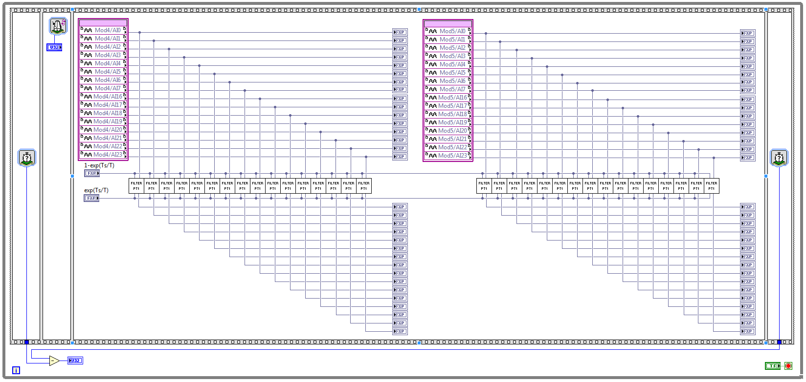
Acquisition of data and filtering on FPGA
Hi all
I have trouble to design a FPGA program for acquisition of data and filtering.
I have two NOR 9205 modules configured to work in terminal mode of DIFF, i.e. There are 32 entries this program must read every Ts seconds. (Ts is the time discretization, i.e. during the period of loop)
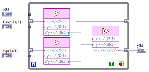
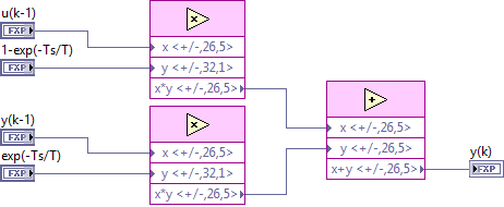
With respect to the digital filter, I implemented a possible simple filter with transfer function G (s) = 1 /(1+sT), which is part of the field of discrete-time equal to y (k) = a * u (k - 1) + b * y (k-1), where u is the original signal, and there is filtered signal. The coefficients a and b are equal to: a = 1-exp(-Ts/T), b = exp(-Ts/T), and T is the time constant of the filter (usually T > 5 * Ts).
The implementation of main program for the acquisition of data and filtering are:
This application is for the digital filter:
However, the problem is that this program cannot take the FPGA resources on cRIO-9114, and Yes, I tried to define the criteria of compilation for the area. I also tried to implement the multipliers in digital filter as lut and DSP, unfortunately without a bit of luck.
Because I don't have that much experience in programming of FPGA, someone has any suggestions how to improve this code to adapt existing FPGA resources?
Best regards
Marko.
Hey Norbert_B,
I managed to solve the problem. First, I changed the reentrancy of Preallocated incoming execution clone to not reentrant execution. As no reentrant VIs have States, I had to use the node of the feedback to the main VI to get u(k-1) and y(k-1). Another important thing is to choose Ignore FPGA reset method in the node of the properties of FPGA implementationfeedback, since in this case, the feedback node uses less resources.
Here is the new main program VI:
And here's the 'filter' VI:
Thanks for the help!
Best regards
Marko.
-
Then as the loop timer Timing vannes_ouvertes. Elements
I would like this while loop to iterate through every second. But it seems that he doesen't recognize the loop timer. What's wrong?
Just found the article to help talking about it: Debugging of FPGA screws using Mode Simulation (FPGA Module)
At the bottom, it says:
Understanding simulated time on the host computer
If you use some FPGA resources and you run the FPGA VI in simulated using I/O simulation mode, the resource uses simulated time rather than real time. Simulated time could be faster than real time according to the number of events that occur during the simulation. For example, if you add a waiting VI (simulated time) for the schema and set the timeout to 1000 ms, LabVIEW does not attempt to delay a second of real time. Instead, LabVIEW delays as long as necessary before performing the next action scheduled in the simulation.
The following resources are using the simulated time on the host:
- Then the loops
- Single-Cycle timed loops
- VI of waiting (simulated time)
- Loop timer Express VI
- Number of cycles Express VI
- FIFO, except DMA FIFO
- Wait on Occurrence with Timeout based on ticks
- Interrupt the VI, during her wait until this that clear is TRUE
-
Hello. I am developing a VI to a FPGA target and I'm trying to make sure who is using the VI can specify the size of an array of input when they instantiate (such as by the presence of an entry to the VI who said "maximum table size" or something). So far, it seems that the only way to do something like this is to go into the VI himself and manually set the size of table for each entry in the table for the VI (open the VI, do a right-click on each input array, select 'Set the size Dimension', choose 'fixed', set number of items). I would like to have a point where I can set the size of all tables at once (as in my case, they are all the same size) and let the person using the VI set it to the right size for which application they use it for (to be clear, let's say I have two uses for this VI and in one case (, I have a table of entry of size 100 and other use of size 1000, I would like to be able to put these in some way rather than do it through the dialog box). Thank you.
It's a little more work, but it could be a case of good use for a memory block on the FPGA. Make it bigger you wait, you need, and then store the actual number of items somewhere. This will allow you to vary the amount of data without consuming large amounts of FPGA resources on an oversized table.
-
I use the element of memory in my fpga code. However, it uses a lot of fpga slices eventhough I chose the memory implementation of the issue of the memory block. I though it should use block of RAM instead of other fpga resources. The number of total slices increases I increase the amount of data in the element of memory. It seems that using slices of fpga. I joined the project in LabVIEW FPGA and FPGA VI with this post. The target FPGA is SMU-7965R. Thank you for your help
LabVIEW FPGA needs to logic on the fpga to take care of the communication between the chip and your host, as the communication of control/light, logic of installation for the dma channel. While LabVIEW FPGA offers ease of use, there is a fee to pay. For most of the time, this cost is acceptable compared to your actual application.
-
Just a general question about gaps in my knowledge. We used a fixed point in the Rio, which is fine. If I do some basic math, say the multiplication of two numbers in the format 20,4 IE integer size 4 and 16 bits after the decimal point and then I get a number of 40.8. Should I re - convert this back to 20.4 or can I leave it and just continue. LabVIEW will make space for all the variable solutions or should I do it manually? I can see if I'm doing a lot of multiplies and adds the numbers get bigger and bigger.
Also, I saw an article where the programmer made the move to the right and chipping itself but the fxp block for me? for example I multiply two 8.4 numbers and get a 16.8 who do I shift to the right and re-scale. What is recommended for the addition, division, and multiplication.
Thank you
I don't know what you're asking here. What do you mean by, "LabVIEW Will make way for all the different solutions?" By providing the result as a value of 40.8, LabVIEW is to ensure that there is enough space for any results. You can continue with this value, but afterwards, you should it retract. With number requires more bits more FPGA resources, and there is a maximum number of bits that can be used to store a value. It is up to you to know how you want to handle this scaling. Sometimes, it is more important to preserve the most significant bits and lose resolution. In other cases, you can know in advance the normal range of entries and can accept the overflow for unusual entries in order to maintain the resolution for typical values. There is no specific best practice. See warnings and recommendations for the use of fixed point numbers and.
-
Undocumented tags FlexRio Adapter MDK ExampleIOModuleCLIP.xml file
The sample file "ExampleIOModuleCLIP.xml" in the Apapter FLexRIO MDK modules, I found the tags of theses that I can't find documentation on.
What they are?
IOModuleID:0xFFFF0000
FlexRIO-IOModule
Hello OveNystas,
The tags you mention are documented in the manual of FlexRIO MDK. I have included some additional General information below, but you can find the answers to your questions in the manual MDK.
In the future, please use the e-mail address included in your SDK Module (MDK) NI FlexRIO Adapter user manual to send your questions directly on the FlexRIO MDK support team. This group has experience with FlexRIO MDK specific questions such as this. National Instruments always improving and working on new versions of the FlexRIO MDK. So, please do not hesitate to use the support email address FlexRIO MDK manual to send me any comments you have about the content of the manual.
Additional information:
FlexRIO uses half-bridge CLIP to create an interface between the adaptation FlexRIO module and the module FlexRIO FPGA. CLIP half bridge is similar to the user CLIP is that it allows your FPGA VI interact with custom VHDL code. We'll find a CLIP using LabVIEW user documentation (help LabVIEW > FPGA Module > FPGA Module Concepts > using VHDL Code as a component-level IP).FlexRIO is the only target of LabVIEW FPGA that supports the half bridge CLIP added on user CLIP allowing the user to interact directly with IO FPGA resources that. Half-bridge CLIP requires that you add a few extra items for your files of CLIPS to ensure that it interacts correctly with the hardware interface. FlexRIO MDK manual is designed to provide all the information, as a hardware designer must create an adaptation module FlexRIO. This includes electrical considerations, mechanical considerations and a section on the passing of half-bridge CLIP.
-
Resources on Rio fpga using the NI 9403 module
I use a CRIO and it works very well with my A/D and D.-a. When I add an e/s digital NI 9403 module, it eats all my resources even if I don't use all that in the circuit! Is there a way where I can use say only 2 or 3 pins e/s and not other use without him swallow all my resources.
I found the problem. When I added the module e/s I used the mode of discovery and he went. It seems it went past Scan mode for some reason any. When I moved the unit on Solution Explorer up next to two other files, I had made A/D D - A mode FPGA, he changed his mode of FPGA itself and then I could remove I/O pins as required. The icon, then changed when I pulled a PIN on my FPGA block diagram and everything was ok.


Maybe you are looking for
-
Stuck on the Apple Logo screen
My phone froze so I restarted. It got stuck on the apple logo screen and I tried to restore it. When I have it plugged into my laptop it would not restore because my boot drive is full. I tried to remove as much as I could turn off my laptop and empt
-
HP Pavilion Touchsmart 23 NO KEYBOARD not WORKING!
Well, I called HP, Logitech, Microsoft, you name it. I recently bought a HP Touchsmart Pavilion 23 at our local office depot. When we started to install everything and realized that a dongle is not included with the keyboard and mouse. I called Of
-
How to remove the old compressed files? I have over 200,000.
After being run-up disk cleanup, I show more than 200,000 old compressed files. How can I remove them?
-
Problem with uptade credit card
Hello world.My credit card ends this month. I have a new and try to enter the new number (as well as a new date, etc.) but the system says "there was a problem with the card information entered. Enter another card or contact your bank. »This is inter
-
Windows7, CC2014 8.1Anyone know of any problems with playback of H.264 on Mac file?* Especially if the file was created on a PC thru' SOUL?Strange question I encounter, it is these files play perfectly on my NLE and my laptop... but my Mac colleagues