How data for chart FPGA of DMA Fifo and relaxation
Have a design Question here:
IM using a FIFO DMA here at the flow of data from the target to the host. Side host, I was using the FIFO read Functinon, converting to Dynamic Data and display in a chart in 'real time '. Pretty easy.
However, I would like to make it more functional. The incoming signal is essentially a square wave. I want to trigger on a rising edge, and then graphic permanently the result in the table. I tried to add that 'trigger and Gate' express Vi, but its uneven (see attached photo).
I am on the right track, or should it be done differently? I was not able to find specific examples for this. I think Im getting messed up because my data are read from the FIFO as a table 1 d, 5,000 items at a time. All of the other examples I've found just show the signals that are generated on the host computer already at a fixed frequency.
Thank you!!!
Bones349,
Hello! Some ideas/questions
1.), you could make a detection of edges in your FPGA, saving you a lot of treatment because no no need to spend no relevant data until the host code.
(2.) what you're doing in splitting the numbers before their conversion to the type of dynamic data? I'm not surw what happens there. You can use a data type of waveform instead, because she would have an element of time to your data.
3.) 5000 incidentally both through your FIFO would be fine.
Tags: NI Hardware
Similar Questions
-
Transmission of data to the host of RT to the FPGA via DMA FIFO
Hello
I try to write data from a host of RT on target FPGA using DMA FIFO and then process these data and read then return of the FPGA target to the host of the CR through an another DMA FIFO. I'm working on the NI SMU chassis 1062 q, with the built-in NI SMU-8130 RT controller and target FPGA NI SMU-7965R.
The problem I face is that I want to send three different tables, two of the same size and the third with different size, and I need one more small to be sent first to the FPGA. I tried to use encode dish with two executives in the FPGA VI. In the first image, I read and write the first table in a while loop which is finite (that is, a finite number of iterations). The second frame contains the process of reading and writing the second two tables (of the same size) in a while loop that can be finite or infinite (depending on a control). The problem is that it does not work. 2 arrays are displayed on the front panel of the RT VI host and works well, however, the table that should have been read in the first sequence does not appear on the front panel of the RT VI host. It is not sensible because if it is not passed from the host to the fpga and vice versa then the second image should not have been executed. Note that I'm wiring (-1) for the time-out period to block the while loop iterations until the passage of each item is completed. So the first while loop has only 3 iterations. Could someone help me undersdtand why this happens and how to fix this?
I enclose a picture of the host and the fpga vi.
Thank you.
If you vote for my idea here and it is implemented, you can even omit the loop FOR fully.

(I also propose the RE / IM divided inside the loop FOR and perform operations on complex table before the loop the transpose and reshape .) In this way, you only need one instance of these operations. You might even save some unnecessary allocations table in this way)
-
Hi guys!
I am writing here after many days of attempts without success...
My request is 'simple', send data from the Panel of Labview RT within a DMA FIFO target host. Then the FPGA core receives data and imported through a knot of VHDL processes, and then after the data is pointing to the Labview RT through a target to host DMA FIFO.
I tested my node VHDL simulation mode in Labview FPGA where data sent by a target scope THAT FIFO and just work fine.
But when I try to run the node VHDL in the real target with data from the RT by DMA FIFO basis, it won't. I already do some checks:
-Data are properly sent through the host target DMA FIFO;
-The data are correctly received in the FPGA base;
-The data are correctly sent to the node VHDL;
-Result of the node VHDL are correctly sent to the heart of the RT through the target to host DMA FIFO;
-Result are correcly received in the heart of the RT, , but the result is false and absurd. But I have proof that my node is semanticly correct with my mock test
So my question: are there reasons to see my work VHDL nice knot in simulation mode and not in mode real target with data from the base RT by DMA FIFO taking into account data Transfer between DMA FIFO work well in both sides? Is there some sample available with data send RT FPGA-based via DMA and data processing with a knot of VHDL and returned to the RT kernel to inspire me?
I can't post my screw here because I work for a company, I use a MyRIO with Labview FPGA 2014 target.
Thank you guys! I am available for some details on my implementations.
Afghow.
Hey!
Thank you for your answer but I solved my problem. Indeed, at first, I tried to make a knot of Combinatorics (without clock) pure, but the problem seemed to come from that.
I modified my node in order to incorporate a clock, according to the prescriptions of this white paper: http://zone.ni.com/reference/en-XX/help/371599K-01/lvfpgaconcepts/ipin_prepare_ip/ . And now, every thing seems to work well.
The question remains why the combinatorial node has worked in simulation mode en not in the actual target?...
But for people with the same problem, I suggest add them a CLK and check an edge of entry with rising_edge (CLK) and if it does not, add an input signal to check if the input signals are valid or not.
Afghow.
-
I want to transfer data to my FPGA using a DMA FIFO. The FIFO is 1024 elements, but can I write bigger than that of the side pieces PC? I don't know if the PC actually allocates a larger block of memory for this purpose?
I'm sure that you can set DMA on the side host is greater. There is a node of configuration DMA you can use host-side to define the size of the FIFO on the side host. The size is set in the hardware on the target side.
-
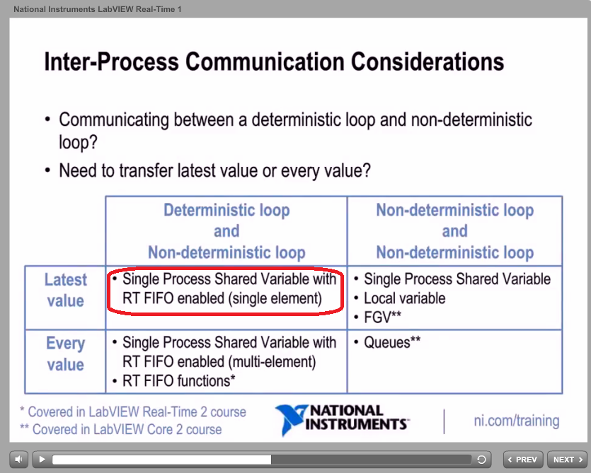
How a shared single process variable be FIFO and single element?
How a variable shared unique process can we both FIFO and the only element at the same time?
I read the NOR recommended for communication between a loop deterministic and non-deterministic loop. He is said to use SVariable ingle-process Shared FIFO and single element. OK I can't have something... because in my mind these two things must be mutually exclusive. How do you have a single item 1?
What 'RT FIFO activé' means, that when you use the variables shared in a timed loop it actually is written to a RT FIFO created automatically.
The key here is that generally shared variables are shared resources and can add jitter to deterministic tasks if another loop uses the variable at the same time as your loop of deterministic.
So here's the takeaway, when shared with RT FIFO active Variables using:
- Normal loops read and write the shared variable in the same way as they always do.
- Call loops read and write a FIFO RT rather
- The data is automatically passed between the RT FIFOs and shared in a nondeterministic loop variable
RT FIFOs exist because their architecture referred to as non-blocking so that when the timed loop trying to access it is guaranteed immediate access to a memory space.
Does that answer your question?
-
Re: Release Date for the Tecra A10 - 18 p and A10 - 15 c
Could someone tell me the release date for the Toshiba Tecra A10 - 18 p and A10 - 15 ° C. What would be the estimated price for these two models.
Thank you
I didn't find the release date of this laptop models.
On the Europe of Toshiba page-> Products->-> Tecra laptops, you will find a whole list of different series and Tecra models.
Right now I find only the info that these laptops will be available soon. -
Sony Xperia Z5 Premium. How make for rotation full screen. Screen and menus.
Hello. I have new premium of z5. I want to know how to get a full rotation in 5.1.1 android
I have the rotation in chrome and the rest of the applications, but the main screen with apps does not run with my activity. also the lock screen does not rotate. then, feeling very unconfortable using the mouse and keyboard wireless BkB10.
I would use view portrait throughout the system, when I need it.
Help, please.There is no way to do this with launcher Sony Home, you will need a third-party application, he asked before, do not forget to send your comments to Sony
-
Validation test for the relationship between network_name, services and relaxation
11g R2 running on RHEL 5 U4
Primary (NO CARS) with a physical Standby (NO CARS)
I'm trying to set up a basic configuration so that the client can ONLY connect to the primary database.
Here's what I think it should all look like
-entry on the primary and Standby physical tnsnames
DMS =
(DESCRIPTION =
(ADDRESS_LIST =
(ADDRESS = (PROTOCOL = TCP) (HOST = PRIMAIRE1)(PORT = 1521))
(ADDRESS = (PROTOCOL = TCP) (HOST = STBY_DR01)(PORT = 1521))
)
(CONNECT_DATA =
(SERVICE_NAME = DG_DMS)
)
)
-the service created on the primary
exec DBMS_SERVICE. () CREATE_SERVICE
network_name = > "DMS",.
service_name = > 'DG_DMS '.
);
-the service created on the primary
CREATE OR REPLACE TRIGGER manage_service after starting on the database
DECLARE
role varchar (30);
BEGIN
SELECT DATABASE_ROLE IN the role OF V$ DATABASE;
IF role = "PRIMARY" THEN
DBMS_SERVICE. START_SERVICE ('DG_DMS');
END IF;
END;
Sounds good?
If this is not the case, can you please explain how to set up.Yes, if you plan to have a service being started on your physical waiting while it is in standby mode, you don't need to create the service with DBMS_SERVICE previously. CREATE_SERVICE. When the waiting becomes the main, Oracle Restart starts the appropriate services as defined by you using the command "srvctl add service d DMSPRMY s DG_DMS-l primary SCHOOL.
If you need a container of service started on a standby physical while it is in standby mode, then you would have still to do the creation on the primary service so that the service is available on the day before.
But in both cases you don't have to create the trigger.
Larry
-
How to choose the maximum number of items for DMA FIFO to the R series FPGA
Greetings!
I'm working on a project with card PCIe-7842R-R series FPGA of NOR. I use to achieve the fast data transfer target-to-host DMA FIFO. And to minimize overhead costs, I would make the size of the FIFO as large as possible. According to the manual, 7842R a 1728 KB (216KO) integrated block of RAM, 108 000 I16 FIFOs items available in theory (1 728 000 / 16). However the FPGA had compilation error when I asked this amount of items. I checked the manual and searched online but could not find the reason. Can someone please explain? And in general, what is the maximum size of the FIFO given the size of the block of RAM?
Thank you!
Hey iron_curtain,
You are right that the movement of large blocks of data can lead to a more efficient use of the bus, but it certainly isn't the most important factor here. Assuming of course that the FIFO on the FPGA is large enough to avoid overflowing, I expect the dominant factor to the size of reading on the host. In general, larger and reads as follows on the host drive to improve throughput, up to the speed of the bus. This is because as FIFO. Read is a relatively expensive operation software, so it is advantageous to fewer calls for the same amount of data.
Note that your call to the FIFO. Read the largest host buffer should be. Depending on your application, you may be several times larger than the size of reading. You can set the size of the buffer with the FIFO. Configure the node.
http://zone.NI.com/reference/en-XX/help/371599H-01/lvfpgaconcepts/fpga_dma_how_it_works/ explains the different buffers involved. It is important to note that the DMA engine moves data asynchronously read/write on the host nodes and FPGAs.
Let me know if you have any questions about all of this.
Sebastian
-
How is managed using DMA FIFO (target host) host matrix
Hi people,
I'm trying to pass an array of values of the host to the FPGA using DMA FIFO. Let's say 20000 items in the table. My FIFO host side can contain only 16000 items or almost. The data will be written element by element regardless of the size of the table or do I need to partition the table in small paintings before writing the FIFO method? Let's say that I write for the FIFO with berries small, 1000-element. The FIFO will read 1 element both of the side FPGA so the stream is blocked until I have at least 1000 free items on the FIFO method write, how he writes every 1000 the next setpoint at the same time? Or target values will be written permanently as soon as the individual elements are erased by the number of available items to write?
Hi Nathan,
Sorry for the late update, but I just thought that I should follow. I followed your advice and try it tested just for me (I probably should I have done it before posting). Turns out that the data table will write even if there is not enough empty elements to contain the table in its entirety. However, it always crashes until enough information is read and erased from memory on the side FPGA for the whole table. So if it's data that are constantly being played, it's always better transmitting data through in the form of smaller tables if you do not want to increase the amount of memory FIFO host OCCUPIES on your system. However, if you can afford the memory while you mentioned, you can always increase the depth of the FIFO on the host side. As I understand it, try to write more big berries to a host to target FIFO buffer does not diminish overhead costs (as is the case with a target to host FIFO) as it still passes an element at a time to the FIFO of FPGA-side without worrying.
Thanks again for your help.
Kind regards
John has
-
How to generate multiple dates for a year [Sunday or Monday or Tuesday]
I want to generate number of holidays for 1 year. based on the box I choose I want to generate all the days in the year. example - if I select the Sunday & Monday I want to generate all Sunday, Monday [dates] for a year.
number of Sundays and Mondays [dates] for a yearWhat I would do, is be a table or an index of collection arrayCollection with number of Flex for the day of the week. For example, index 0 will always represent Sunday.
The State of the check box would change the value of the table at this level, turn MonTableau [0] to true or falsepublic static millisecondsPerDay:int const = 1000 * 60 * 60 24;
private var myArray:Array = new Array;
myArray [0] = false
myArray [1] = true
myArray [2] = true
myArray [3] = true
myArray [4] = true
myArray [5] = true
myArray [6] = falseprivate void GenerateNoofHolidays (): void
{var myDate:Date = new Date();
var startDate:Date = new Date (myDate.fullYear, myDate.month, myDate.date, 0, 0, 0, 0);
var endDate:Date = new Date (startDate.getTime () + (365 * millisecondsPerDay));While (! startDate > endDate) {}
for (var x: Number = 0; x)< myarray.length;="">
If (myArray [StartDate.getDay ()] == false) {}
He has a holiday doing something, that is to say put a full date of this day in an array / collection arraycollection for manipulation}
startDate.setMilliseconds (startDate.getMilliseconds () + millisecondsPerDay)
}
//
}Alert.Show ("\n" + startDate + endDate);
} -
iHi.
My apologies if this is the wrong Board... not sure where it should go! Just to clarify from the outset, I cannot share screws due to issues of IP etc... sigh.
Basically I have a sbRio 9626 and the software that runs on the FPGA to interface with analog converters / digital external. This is done using a machine to States (single cycle loop timed with a structure of business inside, so it passes between cases each tick of the clock FPGA). In one of the cases (the States), I have a little routine that takes data from the ADC and place it in a buffer FIFO of DMA of target-to-host. In fact, there are 4 FIFO DMA buffers to send various information and the value of the sample. It is then read by the software on the host of RT and processed to produce an array of values which I then send to the PC using a shared variable.
What I wanted to check, is that data sent from FPGA to RT host (and PC) are contiguous (that is, I have my right to lengths FIFO). I modified the code FPGA to use a counter instead of the data sampled for the FIFO must simply send numbers in a sequence (1, 2, 3, 4, etc.). I then examine this sequence to ensure that it is correct, and no data has been overwritten.
I think it's the FIFOs, 2, 3 and 4 are very good. FIFO 1 sends data that is continuous but every now and then I seem to get a glitch at random. This glitch is * not * appear to be due to lengths of FIFO, but seems to be an error in the data transfer. For example, I get something like 1, 2, 3, x, 5, 6, 7, y with x and y the seemingly random values. The positions x and y in the sequence are also seemingly random - they have not held in the same place every time. Code written to the FIFO 1 is * exactly * the same thing others - in fact, it's the same group of data being written.
Has anyone seen anything like this before? I am trying to determine if it is due to the goal to receive FIFO or some problem with the shared variable in the network. Any suggestions as to what I could check? It almost seems as if there is IME peaks on the transfer... does not suggest this is the case but it gives an idea of what I see. I'm using Labview 2013 and BIOS on the sbRio is up-to-date. I have sbRio another I'll try again later to see if the problem is specific to a particular board.
It seems that you have found the wrong path here: since you are dealing with the programming of FPGA, which is essentially played woth LabVIEW you should post this question to the Office of LabVIEW or, perhaps, to the Office LabVIEW Embedded
-
Reading of the zeros of a DMA FIFO empty
Hello
I'm having a problem using the DMA FIFO to communicate between my real-time system and my FPGA. I use two DMA FIFO, one-way to the FPGA of the RT system and then vice versa. I can successfully get data to and from each system; However, before, after and sometimes inbetween my data, I'll get a seemingly random assortment of zeros. In the latest version of my code (which I have provided) I read the number of items stored in the DMA FIFO and read only this number to my RT system to try to get the data that I want and no zeros, but this does not work either.
I'm new to both in real-time and FPGA and so it certainly feels like I'm missing something very basic. I tried dealing with this problem by myself well and have had absolutely no success and would appreciate any help.
My equipment includes:
A Dell laptop (used as a host of the user interface)
1082 chassis
Controller of 8133 (running the LabView RT operating system)
7965R FPGA
5781 module for FPGA (not currently in use)LabView 2014 SP1
On the side of RT, you need to use a structure of the case so that you have not read of the FIFO if no data is available.
I would also like to change the flow of network to be inside of your time in a loop until the user interface capturing each data point, as it comes (connect before the loop, close after the loop and write it as the data come from the inside of the loop). This will save memory (which is VERY important in a RT system) since you don't have to set up the table.
You write only as an element in the FPGA. So any sous-suite readings should give you an array of 0 s, causing 0s back upward. You must maintain the Timed Out in the FPGA so that the data will only until to the RT when there is real data to send. Your FPGA code could be reduced to this:

-
Target to host DMA FIFO not compensation when they are arrested
I use a PXI-7841R (Virtex5) and 32-bit data to the host via DMA FIFO transfer. When you read the FIFO on the host for the first time, the data are "stale" (which means that it is not what is currently coming in the FPGA, but what came in a few seconds ago stale). I tried both a stop and a configuration for clear memory FIFO before I use them. Documentation on one or both of these so-called clears the target and host the FIFOs. Does not help in both cases. With readings of the second and the following, FIFO has then 'valid' (same data as it appears on the FPGA entry node). What is curious is that each reading exactly the same thing:
- Stop the FIFO (must erase all data)
- Elements of reading 375 of the FIFO. (repeated playback of the FIFO)
Also interesting: FPGA FIFO is implemented for 255 elements. The first 255 items host-side contain the data "stale" on the first reading. It reminds me of the never erased FPGA FIFO.
Answered by support OR. The documentation for the FIFO, stop and configure FIFO is in error. Cars of documentation will be written against them.
Solution:
These methods remove only the FIFO on the side host. Data FPGA FIFO must be read following until no element.
-
Given to replace my iphone today with a 6s - a trip that I can disable the use of boxes and use a sim card only data for email & web.
If you go to settings > Mobile and less ' use of mobile data for: "turn off all except Safari and Mail
Maybe you are looking for
-
version update 34 displays blank pages unless it is started in safe mode
After the update of v33 34, all pages loaded are empty. The portable and office have the same problem. Uncheck the hardware acceleration did not work. Works in safe mode.
-
Satellite Pro L450D-12 X cut randomly
Hey,. My Satellite Pro L450D-12 X randomly cut out on me all by just work on this topic. I plug in the charger and no light, so never what turns on and it will not be under tension. I disassembled the laptop cleaned up BIG TIME and the mother/logic B
-
How to get the graphics card Intel HD to Satellite C660?
Anyone know how to get graphics Intel HD for a Satellite C660-1JH PSC0LE please?
-
Some strange things have developed to the end that suddenly somewhat concerned me that someone keeps track any activity on my macbook air. I see nothing wrong in the file of applications, but I have to admit that I am somewhat a sucker when it comes
-
LaserJet 500 m551 no project don't print option on Mac OS x 10.7
We use a range of HP LaserJet 500 m551 color printers in my office and it takes too long for the photos to print. When you print a picture of a Mac OS 10.7 (jpg) images, there is no option to print a "draft" or the low resolution copy. The only optio