specifications of clock sbRIO-9651 SoM FPGA fabric.
Hello
I would like to know the following specifications about the clock (clock of fabric) FPGA of the NOR sbRIO-9651 SoM:
-Precision (ppm)
-Aging (ppm/year)
-Temperature (ppm / ° C)
-Skew (ppm)
I couldn't find anything related to this in the specification document.
Is it possible to use an external clock to repalce this one if the specification does not meet our requirement? This clock would be managed by a Board of business custom.
Thank you
Michel
Michel,
The accuracy of the clock is ±50 ppm. You can use an external clock as a source for single-cycle timed loops. The first logical level - things outside SCTLs - is still controlled by the internal oscillator at 50 ppm, but logically or e/s who needs a different precision can be placed in a SCTL and use the external clock. There is some good information on how to import a clock on our developer community material for NI Single-Board RIO and module system. Remember that the quantity of resources used and their frequency toggle will have an impact on the overall jitter of your system.
Thank you
Bryan
Tags: NI Hardware
Similar Questions
-
sbRIO 9651 SoM Unique Identification UID
Dear Almighty LabVIEWers,
our test system I intend using several units of SoM as a control bodies, for this I want to assign the IP address dynamically.
For our current system, we use the UID - the chip inside the CPU and a CRC-32 128-bit in order to get a unique MAC address and generate UID then address IP of this.
My question is: is it possible to get a UID of a hardware component inside the sbRIO 9651?
If not, has anyone had an experience store values to the NAND Flash as a value just read?
Help is highly appreciated!
Dear SerjsVIEW
Do you intend to replace the MAC address of a NETWORK card?
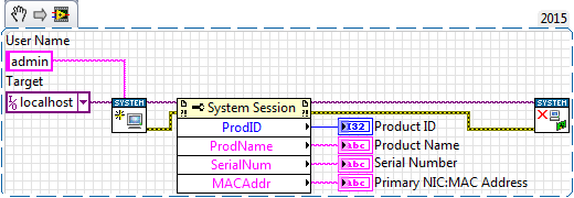
There is no special UID-piece in the SOM to which you have access.
What you can do is to access information system with the 'API Configration system'. There you get information such as ProductID, SerialNumber, product name, MAC address of the NETWORK card.
I hope that helps you.
-
sbRIO-9651: FPGA RS-485 baud rate 230400 beyond? Error-1073807330
I use a sbRIO-9651 and drop the CLIP of FPGA in "Other devices" it shows six Serial1 serial ports... Serial6. The first four are described as "RS-232 serial Port" and the two last "RS-485 Serial Port". On Serial6 (RS-485), I have configured the TX, RX and TX pins activate.
In my .vi on real time, I put my "VISA set up a Serial Port (Instr) .vi" with a baud rate. A works 115200 or 230400 baud rate, but the pace I want to use (256000) generates a run-time error. "Error-1073807330 VISA: (Hex 0xBFFF001E) the State specified, the attribute is not valid or is not supported as defined by the resource."
I suspect the FPGA hardware is capable of 256 Kbps, but I know that if it is a fundamental limitation of the NI UART IP block, or some places I have to change to allow a wide range of transmission speeds (?)
Hello
The maximum rate for these serial ports is 230 400 bps, so there is a limitation on the connection of the UART. In the manual, you will find more specific information if you need it! http://www.NI.com/PDF/manuals/376962c.PDF#page=8
-
How to program a SoM sbRIO-9651
I opened a thread here:
In the ethernet communication between a windows PC and a SoM sbRIO-9651.
I tried to use the sbRIO-9651, but an integrated system of programming seems a little more complex than a cdaq of programming.
I've only sat basic course 1 and 2, so have not sat the FPGA.
I've been following the next link to get me started and used aid in LabVIEW to try to understand how a device OR embedded system programming, but it is a little confusing.
http://zone.NI.com/reference/en-XX/help/373197D-01/sbriohelp/9651_clip/
Advice or stories to help me will be good. Before I think about my project of ethernet communication, I want to start by coming out with devices OR embedded systems.
Hi Dawud-Beale,
My name is Mitchell at National Instruments, and I'm happy to help you regarding your request.
You can consult the links below on the getting started with FPGA programming and get to work with your sbRIO:
Introduction to LabVIEW FPGA: http://www.ni.com/tutorial/14532/en/
CompactRIO tutorial: http://www.ni.com/tutorial/3111/en/#toc3
The sbRIO programming should not be only very different from programming a cRIO, so these articles must be informative.
I hope you find these articles useful for you. Let me know you need help and I'll be happy to do so.
Kind regards
Mitch
-
sbRIO-9651 IO corresponding length
We plan to interface high speed ADC (1gech/s x8bit) that uses a wide interface LVDS (two samples) from 16-bit to a sbRIO-9651. Is there a resource that provides information about the sbRIO-9651 module layout details as worst case length offset series in differential pairs and between differential pairs that exist on the module (independent of our own layout of the Board of Directors)?
Since the interface use a common differential clock and wide 16-bit interface, I'm trying to get a sense tilt the worst case there might be between pairs differential seperatate.
I can they use sheet date architecting to get an idea of the maximum transfer rate, but are there restrictions on the module itself that will limit rates date?
Hi abadobid,
The SbRIO-9651 manual specifications (table 8) should have the details of length sur-module trace info you are looking for.
In addition, I recommend reading the Design Guide for the SOM carrier for detailed techniques, guidelines and requirements for the design of carrier card.
Finally, for future issues are the design of specific equipment for the SOM, we have implemented a dedicated community/forum that will probably be the best place to get help.
Community of developers of hardware for NI Single-Board RIO and module system
Resources for the system OR on the Module
Kind regards
-
Modulation Toolkit screws sbRIO-9651
Hi all
I try to help solve some difficulties with my current developments of the LV.
Currently, I am working on implementing some transmission of packets using sbRIO-9651 interfaced with a programmable TRANSMITTER/RECEIVER. Unfortunately, a few screws (Resample(complex_cluster).vi MT and MT demodulate PSK.vi) run on the sbRIO. These screws are part of the LV modulation toolkit and some dll which fail to load into the sbRIO due to their incompatibility with the platform OR Linux RT-dependent.
Anyone know of workarounds. Any help or suggestion would be welcome.Thank you very much.
Bachir
Bachir,
Is it possible for you to open a DMA FIFO or some other form of data flow of the sbRIO to the host?
A suggestion I have for her resample VI is to use the button Reechantillonner VI, who hails from LabVIEW. I can't confirm that this will work on the sbRIO, but you can try.
The nice thing about the modulation toolkit is that most are open to be viewed by the user. In addition, most of the code is written in LabVIEW. (Not very easily), you could look at the code and try to reproduce them in a fashion that will focus on the sbRIO. You may even be able to find the place where there is no call to a DLL and try to eliminate these dependencies.
Is there a specific reason to use the sbRIO rather than a RIO USRP?
-
sbRIO-9651 reference Carrier Board specifications
There are a little info on the reference card included in the SDK of SOM within the document http://www.ni.com/pdf/manuals/376960a.pdf, but it does not say for example what are the power requirements for the Board of Directors.
I put such a kit in a test area and do not want to use the power supply that came with it. I'm looking for the tolerances of the Executive Board to see what other feeds I can use. I can match the properties of the standard provision of course and it's probably what I'll do, but I expect to be able to go a little outside this range...

Hi MTO.
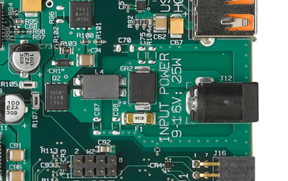
The PCB for the reference carrier has a silkscreen label that refers to the necessary high input power:
9 - 16V, 25W. The documentation for the reference carrier is deliberately light because it is not designed or put on trial for the deployed systems. The carrier of reference exclusively to the assessment office.
See you soon,.
-
Hi all
I work with a system of 9651 sbrio on a module and I am limited by the memory volatile quantity of the device. I could use something like 2 GB of RAM.
Is it possible to create a virtual memory on an SD card, probably through the Linux OS in real-time? Has anyone tried it?
Best regards
Joe
This happened the other day here: https://decibel.ni.com/content/message/107211#107211
-
Specifications of the customization - only some seen in vRA 6.2.0
Hello
When I create a clone of a VC model model I normally specifies a customization script. I have 6 custimaztion scripts starting with the "Base" name... "can I display in vSphere web client on the virtual circuit.
When I search for them through the customization of vRA spec field in a model by using the word 'Base', I have only posted 4. Also if you type the name of one of those missing and save it, then on provision of blueprint, I get an error that the script customization is not found. I can see and edit on the VC. I did vRA collect data of computing resources, but this has no effect.
Anyone has an idea why I only see in vRA some of the specs of the personalization of the VC?
Also, I can see added in December 2015 but miss me one from July 2015.
vRA 6.2.0
VC 5.5 Update 1 c
Thank you
Chris
I don't think you are actually looking for Specs of personalization, you're seeing residual record that you entered in previously as a form that used the same name of backend.
-
With the help of CAE/FGA columns specific null for all, but some users
I was read about VPD and - but there are many examples - I'm having a hard time to get together.
I have a table that - when most users select hand - they should get NULL in a specific column.
This column should only display a limited group of users as one value other than null.
Can someone help me with an example implementation of this?
Any help is appreciated.An excerpt from http://www.oracle-base.com/articles/10g/DatabaseSecurityEnhancements10g.php
CONN sys/password@db10g AS SYSDBA
GRANT EXECUTE ON dbms_rls TO scott;

CONN scott/tiger@db10g

-- Create the policy function to restrict access to SAL and COMM columns
-- if the employee is not part of the department 20.
CREATE OR REPLACE FUNCTION pf_job (oowner IN VARCHAR2, ojname IN VARCHAR2)
RETURN VARCHAR2 AS
  con VARCHAR2 (200);
BEGIN
  con := 'deptno = 20';
  RETURN (con);
END pf_job;
/

-- Using the same policy function as before.
BEGIN
  DBMS_RLS.ADD_POLICY (object_schema         => 'scott',
                       object_name           => 'emp',
                       policy_name           => 'sp_job',
                       function_schema       => 'scott',
                       policy_function       => 'pf_job',
                       sec_relevant_cols     => 'sal,comm',
                       sec_relevant_cols_opt => DBMS_RLS.ALL_ROWS);
END;
/

-- All rows are returned but the SAL and COMM values are only
-- shown for employees in department 20.
SELECT empno, ename, job, sal, comm FROM emp;

     EMPNO ENAME      JOB              SAL       COMM
---------- ---------- --------- ---------- ----------
      7369 SMITH      CLERK          10000
      7499 ALLEN      SALESMAN
      7521 WARD       SALESMAN
      7566 JONES      MANAGER         2975
      7654 MARTIN     SALESMAN
      7698 BLAKE      MANAGER
      7782 CLARK      MANAGER
      7788 SCOTT      ANALYST         3000
      7839 KING       PRESIDENT
      7844 TURNER     SALESMAN
      7876 ADAMS      CLERK           1100

     EMPNO ENAME      JOB              SAL       COMM
---------- ---------- --------- ---------- ----------
      7900 JAMES      CLERK
      7902 FORD       ANALYST         3000
      7934 MILLER     CLERK

14 rows selected.

-- Remove the policy function from the table.
BEGIN
  DBMS_RLS.DROP_POLICY (object_schema     => 'scott',
                        object_name       => 'emp',
                        policy_name       => 'sp_job');
END;
/
The function returns "deptno = 20" so no row corresponding to this condition will show the value of sal and comm, rest will display null value.
IN your case I suppose you want the user to the function that executes the query (select user to double), once you get the user to see if it is a user who is supposed to see the values of columns if yes return "1 = 1" in the case otherwise return "0 = 1".
-
Implementation of I2C in FPGA on SOM devkit
Dear all,
I have this sbRIO 9651 SOM with jury of carrier of reference with which I would like to connect a sensor of MPU 6050 Pmod 5 and acquire sensor data in an FPGA VI and process data in a RT VI. I find it difficult to implement I2C interfacing to FPGA as I am relatively new to FPGA programming in LabVIEW. MyRIO implementation was pretty easy as the API and usage example it was easy to access. Any help would be appreciated.
Concerning
Guenoun
Hello
I found this documentation to be very helpful:
https://decibel.NI.com/content/docs/doc-41410
She described the meaning of in, out and activate. SCL clock series, SDA is given in series. In and out are to read and write data, activate switches between being an input or output pin. It is what explains the wiring in this post on the forum: https://decibel.ni.com/content/message/127591#127591
The I2C bus is high when idle, so out is set to false (bass), but this has no effect because enable is false. In order to drive the bus low, enable is set to true. Now has an effect and driving the bus low. If the bottom of the bus is set to true to activate while the output is held low literacy.
I hope this helps you.
Alex
-
Independent of the 40 MHz clock Onboard FPGA PPS GPS meter
Could you give me some advice or point me in the right direction?
I need to time counter accurate/tick synchronized by GPS PPS synchronization signal.
I got cRIO S.E.A. GPS Module that trigger PPS signal at the bottom of basket FPGA. PPS rising edge signal precisely mark the beginning of the second.
When I measure the number of ticks of 40 MHz clock FPGA embedded in a (PPS) second number of ticks is not 40.000.000 ticks but something like 39,999,800 ticks.
I want to measure with precision time between edges up/down digital signals. Because the clock of 40 MHz FPGA are drifting I can't use it.
How could set up my own witch counter ticks will be put away with signal GPS PPS?
I don't expect that I could provide 40 MHz FPGA on board the oscillator.
Should I create my own counter which will increase the opposite by the value 1.000,005 (40 000 000 / 39,999,800) each tick and this counter will be running timed loop (chronometric 40 MHz FPGA embedded base). Increment the value (1,000...) will be updated every seconds dependent PPS vs FPGA clock drift.
My configuration: cRIO-9025, cRIO-9116, S.E.A. GPS + cRIO module, high-speed DIs NI 9402, RT/FPGA LabVIEW 2011
Looking forward to your hearing you.
PeterHi all
This could help you.
Timekeeper FPGA
- http://digital.NI.com/public.nsf/allkb/EFDC35727D4F2CC086257A0700693003
- https://decibel.NI.com/content/projects/NI-TimeSync-FPGA-timekeeper
(I do not understand how this could be released on 23/05/2012)
-
To use the external clock for SCTL myRIO
Hi people,
I'm trying to find a way to get a 2.5 PSM 16-bit ADC, TI ADS1602, to send data to the device myRIO. Ideally, I'd like to bit Records at 40 MHz in order to obtain the benefit of the PSM full 2.5. I know that I can create an 80 MHz SCTL on the FPGA to create a clock of 40 MHz, but when I checked the clock on an oscilloscope signal, it was obviously greatly degraded by bunch speed limits, so he looked more like a sine wave to a square wave. I doubt it would work for use as a clock signal to drive the ADC since ADC specifications say that eligible jitter is around 100ps.
I can use an external oscillator to drive the ADC, but then I have to find a way to sync the clock with clock FPGA 40 MHz. is there any kind of PLL structure that would allow me to sync the clock FPGA myRIO to an external clock? Is there a way to do a loop simple timed cycle driven by an external clock? Or if I was able to customize the FPGA personality to accept a SPI signal up to 40 MHz (ten times her supported limit...), he would be allowed to use an FPGA to ~ 160 MHz and tell him to taste the SPI line each loop and proceed from there?
Thank you!
Hi 3.14159... ,
The myRIO doesn't have the ability to import a clock to use on the FPGA block diagram for clock loops timed cycle unique (SCTLs). The sbRIO-9651 new coming out week OR (not shipping yet) is the only sbRIO who has the ability to import an external clock in LabVIEW. Many of our products FlexRIO also have this ability.
Like you we have it, you can taste the signal at twice the frequency (or maybe more) to and wait an edge trigger to run a certain element of logic. "" "If you open the example Finder and navigate to hardware input and output" R series "FPGA Fundamentals ' triggers and guard dog" trigger detection, this gives a simple example to do this. Once again, since you are eager to taste 10 times the frequency of support, all bets are off, but it may be worth trying.
-
acquisition of data and processes in FPGA
Hello!
In FPGA, I am trying to acquire analog data (0 ~ 10V) with a specific time clock rising edge of each digital pulse encoder.
I went to get the data on the front, but I don't know how I'd keep th and i + 1 th data.
(Frequency of data is less than 250 kHz)
I have the cRIO-9074, NI 9411 (encode), NOR 9205 (module I),
data
1st, 2nd data, data 3rd 4th 5th 6th 7th... I-1 th, I e, i + 1-th... 1200 e (approx.)
I need every sum of two consecutive data data 1st + 2nd, 2nd + 3rd, 3rd + 4th, l - 1 e + i Thess,... th + (i + 1-th)... 1199 th + 1200 e (about)
On the process of two consecutive sum.
[i - 1 e + i th] / [a value] + [the other i e amount of different data acquisition] = 1199 set of data (up to 1200 th data)
and then
all data across data (data from 1199) will be worth.
Thank you very much!
All tips are welcome!
Sincerely,
Hyo
Looks like a simple feedback node will do the trick.

-
example simple + huge delay + fpga
Hi Member
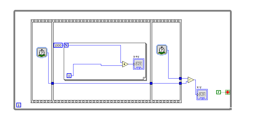
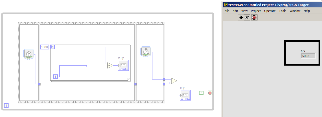
I'm trying to caclute number of clock for this example caculate, the delay for the ' ' «for loops with 1000 run»»»
After complition process the vi was executed on fpga and read the number of cycles in the pc with the real time and the number of clock was 5002 clock as shown below
What is c?
is their any wrongdoing in my vi
mangood wrote:
So if a system (add many components, sub) and put this system inside the ""while loop"
Inverse of the period of the loop will be the frequency of the loop. Or frequency system is true!
-----------------------------------------------
I'm sorry for the stupid question, but my work on the architecture of the systems so these parameters is crucial and important for me.
I left my old job on tool company xilinx ISE because the design of the system to take a lot of time so I now moved into labview fpga, its amazing especially in the optimization process, but the clock Concept here is very weak and totally confused.
It's a different clock concept that most use of FPGA designers, it's true (I am trying to learn about it at the moment I'm doing some work software - C, not LabVIEW - on a processor clocked inside an Altera FPGA). For a normal programmer it makes sense - it works just like it does on a desktop computer. On a desktop computer you do not need to know how fast the processor is, you just need to know how long it takes your code to run.
I don't know what is the distinction between the loop and frequency of system for you. There could be other components of the system that are running at a different frequency that you don't see, but are required by the LabVIEW environment (for the acquisition of data or communication with the host processor), but your code inside the loop runs at the level of the loop which can be measured with the number of cycles.
Maybe you are looking for
-
Problem Installation plug Adobe Flash Player 10.3.183.7
On several sites, I was alerted that I need to install the plugin Adobe Flash Player 10.3.183.7 to see everything correctly. When I select the button install, I get the message that it could not be installed, and I had to install it manually. By sele
-
Satellite L750D-14R Win 7 reluctant to start, freezes when it does
Hi, my daughters L750D-14R has developed a fault. I searched this forum and did not see a solution.(running Windows 7 Home Premium) Yesterday he ran checkdisk at startup and froze. He does this every time on a hard reboot. I tried: F2 - in the config
-
Computer HP laptop Pavilion DV6t has Intel wireless display?
I am considering Netgear Push2TV and it requires Intel wireless display.
-
Windows install will start automatically on reboot
Windows install lights automatically restarts and then goes manic. I have to stop it by (several tries) Task Manager. I tried to register again without success. My computer works fine between these episodes above. I would like to uninstall (or ren
-
How manually to disable source outpoint changes three points in the timeline
Hi all, I am a passionate Editor, cutting more and more on the Prime Minister and to love him.I know that in this latest version of the Prime Minister, there are options on how you want Prime Minister by default if your source has an input / output a