Synchronization of FIFOs in FlexRIO SMU-7962R
I am acquiring data digitized using 16 channels NI 5751 on SMU-7962R. I have to do it as fast as possible that of why I use 4 FIFOs with depth of 32768 elements and width of 64 bits (each symbol takes 16 - bit).
I recently discovered that the FIFO is not synchronized. There is somehow arbitrary delays between different blocks of data from the FIFO. The delays remained the same, at the time of purchase. I think it is mainly due to the fact that I'm not rinsing the FIFOs correctly during the initiation.
Is it possible that I can solve this it such that the FIFO is synchronized.
I enclose the folder of the project, also the charts for Host.vi and FPGA.vi
Any help will be very appreciated!
Appreciate the feedback!
Your previous post made me understand that it is indeed possible to increase the depth of the FIFO on the host side (I have 12 GB of RAM, IE I have virtually no limits). This allowed me to redevelop the FPGAS such as I now use a simple FIFO instead of four to communicate with the host (only running at 10 MHz instead of 50 MHz sampler, also helped, because I had need of 5 ticks to serialize data).
So, the problem is solved using a simple FIFO instead of four. Thank you Christian for pointing me to finger the right directon.
Tags: NI Software
Similar Questions
-
Unable to access SMU-7962R + OR-5734 in LabVIEW
Hello
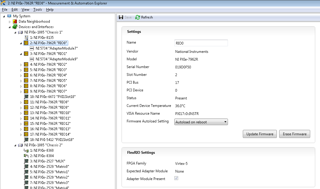
I have already developed a SMU system that uses FlexRIO. This has worked well. FlexRIO devices appear in MAX OR as follows (note that FlexRIO modules have yellow icons of FPGA, and their adaptation modules are shown):
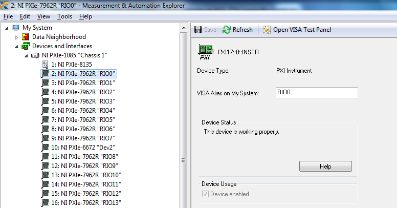
I'm now trying to build an exact copy of this system. I put together a together identical material, and (far as I can tell) I installed all the same components as the original system (using the NI Developer Suite 2015 DS1 set). However, something is not quite right. Here's what MAX OR shows me in the new system (note that FlexRIO devices now have generic grey icons instead of yellow icons of FPGA, and adaptation modules are not visible).
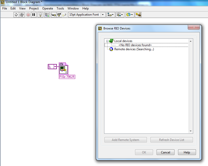
In addition, the LabVIEW code that I developed for the original system generates a runtime on the new system error "NOR-RIO: (Hex 0xFFFF0928) the name of the supplied resource is not valid in a resource name of RIO or the device was not found." Use MAX to find resources appropriate for the expected device name. " LabVIEW is unable to find RIO devices:
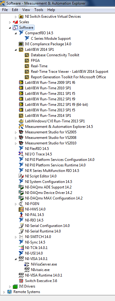
Here is the list of software installed on the new system:
I also installed NI FlexRIO Adapter Module Support 14.1.0 (who does not appear in NI MAX). Can anyone place what Miss me?
Thanks in advance!
Hi David,
2 controllers had exactly the same BIOS (version 1.2.0f0), which was the latest version for the SMU-8135.
It turns out that, even if I had installed the drivers, Windows had not "registered" (?) the drivers properly for some reason any. There was a lot of articles in "Device Manager"-> "devices OR-RIO":
- x 15 "NI SMU-7962R", were all OK
- x 15 "NOR-RIO FPGA Device", all had yellow exclamation on them.
I clicked "NOR-RIO FPGA Device" and selected "update driver software...". '-> 'Browse my computer for driver software'-> "Let Me pick from a list of drivers on my computer"-> 'NI - RIO FPGA Device'. After that I did "device of FPGA OR-RIO", all 15 exclamation points disappeared and I could use my FlexRIOs correctly.
-
NOR-5781 Baseband Transceiver and OR SMU-7962R (FPGA)
I'm looking for an example of code to transmit videos using OFDM in LabVIEW between two different units of the PXI. I have two different sets of NOR-5781 Baseband Transceiver and NI SMU-7962R (FPGA) installed in two PXIs. One is the sole issuer and another is to be alone receiver.
Are there examples of code to trasnmit video with the help of these above mentioned devices preferably via OFDM in LabVIEW.
Thanks in advance.
Hey Joseph,.
If you look at the 5781 start-up project, you will see that the analog input and output of the sections of the code are separated. You will want to remove the section of code of analog output of the side Rx and remove the analog input on the side of Tx section. At this point, you would have a functional code that would send signals to a chassis to another, you simply add this necessary to the wave before you write it on the device of modulation and demodulation subsequently shape wave after receipt.
The examples are intended to be a starting point, and I think that you can access your ultimate goal without much change (remove unnecessary parts of the code and the addition of modulation).
-
Invalid values obtained sporadic FlexRIO card
Hello
I can't acquire the data of my FlexRIO (SMU-7962R + OR-5734). I write custom code instead of using FIDL building blocks, because the FIDL requires a design of master-slave to trigger synchronized, while I need each FlexRIO card to activate it.
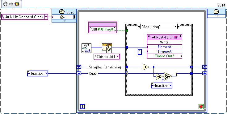
In short, this is a small test case (I tried with a 40 MHz clock and a clock of 10 MHz, with the same results):
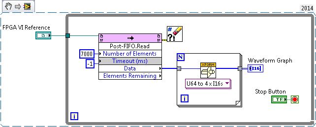
FPGA
Host
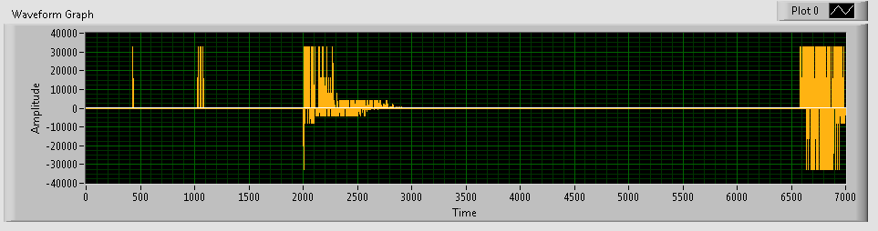
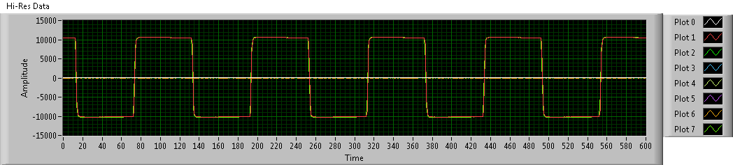
While most of the output looks ok (i.e. the look of signals as input signals), I have several bursts of corrupt samples. I often get spikes that equals the I16 max/min value, although there are cases of non-max tips too.
Interesting fact:
- Each FlexRIO card seems to have exactly 1 channel of misconduct.
- The channel varies from cards (for example RIO1 gets spikes in AI0, while RIO2 gets spikes to AI3)
- When I repeatedly trigger acquisition on the same card, I see a very similar form 'noise' every time. Different cards produce different forms "noise".
- I see spikes when I use the FIDL pre-built instead of my own code examples (maybe I need to make some sort of synchronization?)
Screenshots below.
- Orange graphics are supposed to be zeros.
- The green graph is supposed to show a pure sinusoidal signal.
What could be the problem and how can I solve this problem?
Thank you!
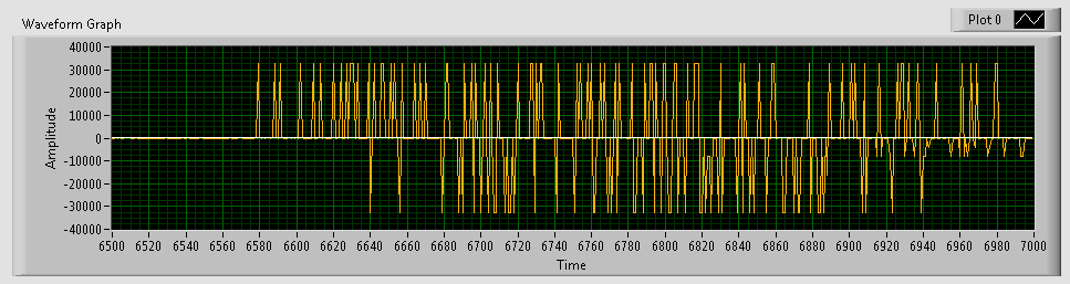
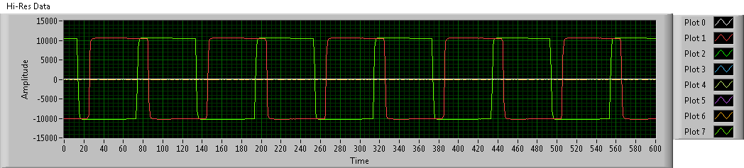
Zoomed in
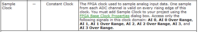
You must acquire the 5734 data in the area of the sample clock. Reading from the node HAVE in any other field clock causes the glitching you see.
-
Advice on the Organization of the modules in a system of 2-chassis SMU
Hello
Content of the system
We have a system which consists of:
- 2 SMU-1085 hunts, connected via an SMU-8384/SMU-8360
- 15 maps FlexRIO (SMU-7962R + OR-5734), to acquire data at 10 MHz
- 1 function (SMU-5412) generator
- map 1 calendar (SMU-6672)
- Other cards (switches and low-speed i/o)
Use cases
- In a mode of operation, we need 60 FlexRIO channels to listen to at any time. When a channel exceeds the threshold, all 60 channels must be simultaneously acquired and recorded on the disc (i.e. each FlexRIO card must be able to trigger in all 15 acquisition cards)
- The other mode of operation, to generate a pulse of the SMU-5412 and acquire at the same time all 60 FlexRIO channels since the moment the fire pulse.
Question
Essentially, we have 17 maps of conservation (15 FlexRIOs + 1 function generator + 1 card calendar), but only 16 cards can fit in a frame (because 2 slots are ocupied by the on-board controller and MXI-Exprress card). Thus, one of these must be on the other chassis. Then the two obvious options are:
- FlexRIOs so that the function on the 1st frame generator, calendar card on the chassis from the 2nd.
- FlexRIOs more map timing 1 chassis, generator of functions on the chassis of the 2nd.
Does it matter which option we're going for? Can we get the benefits of performance or ease of coding be it?
Thanks in advance!
If all that you want to this topic the accuracy of the clock, there an entry on the back of the SMU-1085 for an external clock of 10 MHz and a 10 MHz clock rate. So everyone can use the same clock.
But you worry about triggering. So I see two real options:
1. turn all that must trigger the other in the same chassis. That would mean putting the source of synchronization in the second frame and using the reference I/O on the chassis clock to share clocks.
2. get a second synchronization module. The module should have PFI lines so that you can share trigger signals. I would still use the reference I/O on the chassis clock in order to ensure that everyone uses the same clock.
-
My specs are:
-Chasis SMU-1082
-FlexRIO SMU-7962R
-MRF custom calendar card
The MRF pushes its clock to the PXI_CLK10_IN with own clock at 10 MHz.
I use several SCTL to Council FlexRIO with multiple clock sources. Availiable clock sources are (also see attachment):
-40 MHz on-board clock
-PXI CLK10
-Clock 100 MHz
-Clock 200 MHz
-Clock DStarA
I can't get my hands on the information what are the sources of clock of 100 MHz and 200 MHz clocks. Who are special oscillators to the Board of Directors? Are the clocks 40 MHz clock PLL - ed or the PXI CLK10 PLL - ed?
After some additional searching on Google, I got my answer: http://zone.ni.com/reference/en-XX/help/372614J-01/target5devicehelp/pxie_base_clocks/
-
SMU FlexRIO DMA FIFO host read the FIFO overflows broadband bandwidth/DMA issues
I'm working on an application that uses 2 modules FlexRIO, and 2 LVDS digital I/O adapters. I'm driving each of the SDC A/SDC B ports on LVDS 16-bit data at 50 MHz adapters. The FlexRIOs are expected to receive the data and write down them on four targets-to-host DMA FIFO (one per connector SDC), or two by FlexRIO. The host reads the FIFO and brings together a series of tables each FIFO output 2D. Ultimately, the individual tables (we're each a quarter of single image) will be assembled in simple images, but I haven't gotten that far yet.
The duty cycle for the data is about 80% (in other words, I'm only transmit data to the FlexRIOs 80% of the time, the rest of the time the transmitters are disabled), so the flow is about 80 Mbytes/sec/port total invasion, or 320 MB/s on the four FIFOs DMA. I find that the acquired data gaps sometimes inside that line up along the length of the material part of the DMA FIFO in FlexRIO modules. In other words, if my memory FIFO DMA are set to 65535 length, I'll see a break in the data acquired at the word of data 65536th. Data is a waveform of sight, which is essentially just a counter, so it's easy to see the break in the model. For the words of first 65535, adjoins the data, then from Word 65536 model is discontinuous and starts counting again from there, contiguously. At the beginning of the acquisition, the FIFO is erased: the beginning data read from the FIFO is always aligned correctly, so I know that the process starts at a good point.
The error is not always the case: sometimes I get continuous data through the point 65536. In addition, the error occurs independently between the four FIFO: on a particular race, a FIFO could have data of interest and some bad. Rarely, all four FIFOs have good data.
The fact that the gap of the configuration is to the point even the depth of the FIFO DMA tells me that fills the FlexRIO FIFO, the FPGA hardware without the system managing to move to read, which means that the data gets dropped during the period that the FIFO is full. Then transfer to the host comes into action, there again is the space in the FIFO, and the data is once more contiguous in FIFO memory for a large amount of data (I have not yet tried to locate a second gap in the data of a single acquisition). It seems therefore that the host doesn't have enough bandwidth between the FlexRIOs and the host of RAM to prevent the filling FIFO, or comes along some software process on the host that is temporarily stop the ability to instantly transfer.
Are at - it a specification for the SMU flow system that would indicate that we are trying to use too much bandwidth? Or are there priority controls on DMA FIFO that would allow us to raise the priority of the FIFO transfers as they are guaranteed to go in preference to other system tasks?
System Specs:
SMU-1075 chassis
SMU-8135 CPU
2 SMU-7962R FlexRIO modules
2 digital i/o modules of NOR-6585
LabView 2012 32-bit SP1 version 12.0.1
A suggestion of an applications engineer of NOR and some experimentation has solved the problem. It turns out that I was calling the method FIFO of DMA stop just before the outbreak of the transmission of the data via a control for the FPGA FPGA VI. I did this in order to clear the FIFO before you begin data acquisition, but I didn't know that this method disables also transfer data between the memory FlexRIO and host. Following this call, I trigger the FPGA code to start filling its FIFO and then begin reading. Calling the Read of FIFO of DMA apparently light up the transfer back, but it seems that the host VI has been randomly slow down enough to move to the bed such as filling the side FlexRIO FIFO and dat would be lost. I changed the host VI to insert a FIFO method call start before the trigger for the FPGA signal, and the problem is now gone.
-
[FlexRIO] Start-up to synchronize several clocks sample
Hello
I tried before, two different (SMU-7962R + OR-5734) FlexRIO card reading in the '40 MHz Onboard Clock' or 'PXI_Clk10' areas of clock. Trigger has been achieved by simply looking for a rising edge on PXI_Trig0:
This produces seeds, but there has no inclination (or constantly tilt at least) between the two FlexRIOs - I sent a pulse train duplicated in the two cards, and the triggered-acquired waveforms were still at the stage:
To avoid problems, I went to examples of clock (IO Module clock 0). Unfortunately, the clocks of the sample between the two FlexRIOs had nothing in common, so the acquired waveforms have been is out of phase. Worse still, the phase difference changes with each release:
Looking at the implementation of the library of the synchronization of the FIDL, the classic technique for synchronization of multiple cards FlexRIO seems to be built around synchronization master-slave (my observation is correct?). I was wondering: is there a way to simply share a sample clock shared between cards (like what the 40 MHz embedded clock was doing before), as described in http://www.ni.com/white-paper/11369/en/ ? (I think I understand the disadvantages associated with sample clock synchronization, but I'm willing to try for now).
Thanks in advance!
Hi JKSH,
Page 9 of the Manual 5734 described the different synchronized methods that can be used the 5734. You can synchronize either sample clock of each module to a clock available through your chassis backplane (for example, DStar_A) by allowing the IOModSynClk in 5734 properties (available the Details category) or use an external clock through the Clk port on the module. Activation of IOModSyncClk is probably the best approach and will lead by examples of clock on each module e/s being PLLed on the clock of the town - which must synchronize the clocks of the two sample together.
Let me know if you have follow-up questions.
Kind regards
-
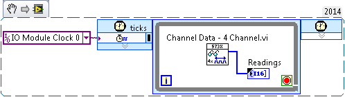
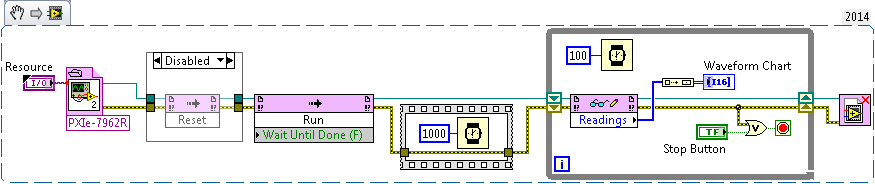
Understand how to set up and use a sample FlexRIO clock
Hello
Following this discussion on inputs glitching, I learned that I need to use the area of the sampling clock to read nodes to HAVE it in my 5734 OR. So I right click 'FPGA Target'-> "New FPGA Base Clock" and selected "IO Module clock 0". In general, I followed the instructions at http://www.ni.com/pdf/manuals/375653a.pdf
Issues related to the:
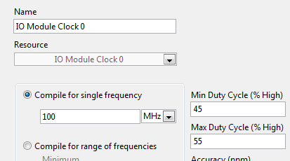
- I noticed that, regardless of the value I put in "Compile single frequency", timed loops using this clock works at 120 MHz. Should it?
- I want to gain at 10 MHz, no 120 MHz. is there a way to create a clock derived from the sample clock? (Right click on the clock gives me not the option "New FPGA derived Clock")
- In the example of the FIDL, engine of CQI on 5734 SMU - 7962R.lvproj, 'IO Module 0 clock' is configured to be compiled to "100 MHz" instead of 120 MHz. is there a meaning behind this value? (# 1, I understand that the value is ignored)
- The code example below, I get "error-61046 occurred to read/write control" unless I have excluded the "Reset" of the VI host node. This problem does not occur if I use on-board 40 MHz clock instead of the clock of Module e/s 0, (although I'd get glitched data). Am I wrong configured something?
- In my current, more complex program, I get the same error even with disabled node, if I stop and restart the host VI - but the next attempt would succeed.
- I have attached the sample file project, the screw and bitfile, where they are useful.
Hi FKSH,
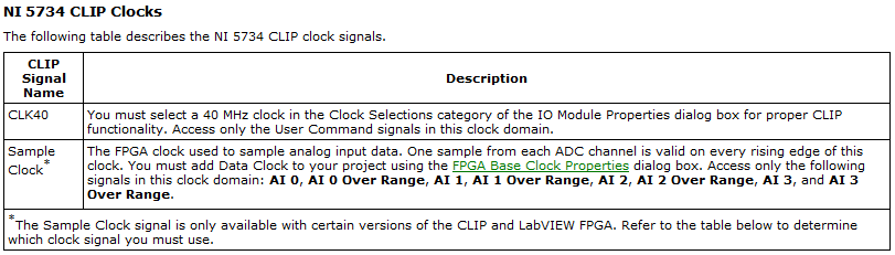
You are right that you must Access your e/s on the 5734 NOR in the area of sample clock:
(this information is by using LabVIEW for the CLIP of 5734 OR)
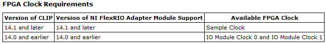
It is a clock Module e/s 0 or sample clock based on your version of the FlexRIO driver you have installed. Based on your statements, looks that you use LabVIEW 2014, so be sure to have FlexRIO 14.0 or FlexRIO installed 14.1. If you have FlexRIO 14.0 or earlier, the sample clock will be IO Module clock 0. If you have FlexRIO 14.1 or later, it will be the sample clock:
(also of the documentation NOR 5734 CLIP in help)
The only support for sampling rate is 120 MHz, unless you use an external clock CLK in and it must be between 50 and 120 MHz (see page 9 of the Manual). If you wish to purchase to 10 MHz, the best thing to do would be to sample the e/s to 120 MHz and then decimate the data by a factor of 12 (keep all 12 data points only and throw out the rest).
Regarding the FIDL, I'm guessing that you're referring to the configuration in the properties of the clock:
This configuration is not actually change the frequency of the clock. The compiler uses this value so that the logic can operate at the specified frequency, but the real clock is provided elsewhere (in this case, the FAM).
Finally, I saw error-61046 occurs more often because of the configuration of the internal clock. Make sure you use the clock on the right as the only cycle timed loop source as I mentioned above. In general, I do not recommend write directly on a 120 MHz indicator, as there are a lot of other logic that needs to be done in order to update the indicator. The data are sent to a domain different clock under the hood, so you can actually update the data and I suspect that there are some conflicts with the clocks. You also lose data as the host won't be able to read all the data before it gets crushed. Instead, I would use DMA FIFOs if you need all the data you acquire or to send the data to a different loop which will be responsible for the update of the indicator in a slower clock domain.
In general, I recommend always that the start-up of the examples in the Finder as a good place to check if the equipment works properly and as a reference for the correct configuration. Once you compile the code, you should be able to run it natively to acquire some data. "" "These examples will be under input and output hardware" FlexRIO "Modules e/s ' NI 573 X ' NI 5734.
Best regards
-
SMU-7975R with FPGA Kintex-7 - LVDS problem
Hello
I developed a custom RIO FLEX module (Digitizer18, 0xAB66 - vendor id) and try to use it with the card 7975R-SMU-FPGAS (FPGA Kintex-7)
I have a problem, try output LVDS signal via aUserGpio (61) and aUserGpio_n (61).
These pins are not K7 capable clock, but I used this module FLEX RIO with SMU-7962R (Virtex-5 FPGA) where these pins are capable REGIONAL clock and it worked fine.
Kintex-7 it compiles without error, but I see no signals on the pins aUserGpio (61) and aUserGpio_n (61), although its switching State is ADC2_FSM.
Is it possible to use pins that is not capable of WHAT LVDS output or I am condemned to use MRCC clock or pins SRCC?
Thank you
My xdc file (aUserGpio (61) and aUserGpio_n (61) belong to the 18 Bank):
set_property IOSTANDARD LVDS_25 [get_ports {aUserGpio [61]}]
set_property FAKE DIFF_TERM [get_ports {aUserGpio [61]}]
set_property IOSTANDARD LVDS_25 [get_ports {aUserGpio_n [61]}]
set_property FAKE DIFF_TERM [get_ports {aUserGpio_n [61]}]# all unused pins Bank 18 are LVCMOS25
set_property IOSTANDARD LVCMOS25 [get_ports {aUserGpio [49]}]
set_property BUNCH SLOW [get_ports {aUserGpio [49]}]
set_property DRIVE 8 [get_ports {aUserGpio [49]}]
set_property BIO FAKE [get_ports {aUserGpio [49]}]...
part of my clip to vhd file (because it's too big and all other LVTTL logic works very well except LVDS):
attribute dont_touch: string;
Signal ADC2_CNV_buf: std_logic_vector: = '1';
attribute dont_touch of the ADC2_CNV_buf: signal is 'true '.OBUFDS_ADC2_CNV: OBUFDS
map of port)
O-Online aUserGpio (61)-Diff_p output (connect directly to the port of higher level)
OB-online aUserGpio_n (61)-Diff_n output (connect directly to the port of higher level)
I have-online ADC2_CNV_buf - the input stream
);....
process (LVDS_CLK) - 200 MHz
Start
If LVDS_CLK' event and LVDS_CLK = "1" then
ADC2_FSM case is
When s0 =>
If ADC2_CNV = "0" then
ADC2_timer1 <= (others="">' 0');
ADC2_timer2 <= (others="">' 0');
ADC2_CLK<=>
ADC2_READY<=>
ADC2_CNV_buf<= '1'="">
ADC2_FSM<=>
end if;
When s1 =>
If ADC2_CNV = "1" then
ADC2_CNV_buf<= '0'="" ; ="" ="" ="" ="" ="" ="" ="">
ADC2_RESET<= '1'; ="" ="" ="" ="" ="" ="" ="" ="" ="">
ADC2_FSM<=>
end if;
When s2 => ADC2_FSM<=>
When s3 => ADC2_FSM<=>
When s4 => ADC2_FSM<=>
When-online s5
ADC2_CNV_buf<= '1'="" ; ="">
ADC2_RESET<=>
ADC2_FSM<= s6;="" ="">
When-online s6
If ADC2_timer1< x"28"="" then="" --="">
ADC2_timer1<= adc2_timer1="" +="" 1;="">
on the other
ADC2_FSM<=>
end if;
When s7 =>
ADC2_CLK<= not="">
If ADC2_timer2< x"24"="">
ADC2_timer2<= adc2_timer2="" +="">
on the other
ADC2_READY<=>
ADC2_FSM<= s0; ="" ="">
end if;
When other => ADC2_FSM<= s0; ="">
end case;
end if;
complete the process;-the host uses the flank amount of DCO± to capture D±
process (UserGClk2, ADC1_RESET) - echo DCO2 clock
Start
If ADC1_RESET = "1" then
ADC2_READ_FSM<= s0; ="">
ADC2_BUF <= (others="">' 0');
elsif UserGClk2' event and UserGClk2 = '0' then - host uses the flank amount of DCO± to capture D±
ADC2_READ_FSM case is
When s0 => ADC2_BUF (17)<= not="" d2="" ;="" adc2_read_fsm=""><=>
When s1 => ADC2_BUF (16)<= not="" d2="" ;="" adc2_read_fsm=""><=>
When s2 => ADC2_BUF (15)<= not="" d2="" ;="" adc2_read_fsm=""><=>
When s3 => ADC2_BUF (14)<= not="" d2="" ;="" adc2_read_fsm=""><=>
When s4 => ADC2_BUF (13)<= not="" d2="" ;="" adc2_read_fsm=""><=>
When s5 => ADC2_BUF (12)<= not="" d2="" ;="" adc2_read_fsm=""><=>
When s6 => ADC2_BUF (11)<= not="" d2="" ;="" adc2_read_fsm=""><=>
When s7 => ADC2_BUF (10)<= not="" d2="" ;="" adc2_read_fsm=""><=>
When s8 => ADC2_BUF (9)<= not="" d2="" ;="" adc2_read_fsm=""><=>
When the s9 => ADC2_BUF (8)<= not="" d2="" ;="" adc2_read_fsm=""><=>
When s10 => ADC2_BUF (7)<= not="" d2="" ;="" adc2_read_fsm=""><=>
When s11 => ADC2_BUF (6)<= not="" d2="" ;="" adc2_read_fsm=""><=>
When s12 => ADC2_BUF (5)<= not="" d2="" ;="" adc2_read_fsm=""><=>
When s13 => ADC2_BUF (4)<= not="" d2="" ;="" adc2_read_fsm=""><=>
When s14 => ADC2_BUF (3)<= not="" d2="" ;="" adc2_read_fsm=""><=>
When s15 => ADC2_BUF (2)<= not="" d2="" ;="" adc2_read_fsm=""><=>
When s16 => ADC2_BUF (1)<= not="" d2="" ;="" adc2_read_fsm=""><=>
When s17 => ADC2_BUF (0)<= not="" d2="" ;="" adc2_read_fsm=""><=>
When s18 => ADC2_READ_FSM<=>
When other => ADC2_READ_FSM<= s0; ="">
end case;
end if;
complete the process;
ADC2_DATA<= "00000000000000"="" &="" adc2_buf="">I've made a few changes to TestCLIP.fam:
...
[FlexRIO-K7IOModule]
DefaultCLIP = TestCLIP
VccoLevel = 2.5...
And my xdc file now looks like this:
# Set the voltage from Bank to Bank 18.
#set_property IOSTANDARD LVCMOS25 [get_ports-filter {IOBANK == 18}]set_property IOSTANDARD LVCMOS25 [get_ports {aUserGpio [*]}]
set_property IOSTANDARD LVCMOS25 [get_ports {aUserGpio_n [*]}]
set_property IOSTANDARD LVDS_25 [get_ports {aUserGpio [58]}]
set_property IOSTANDARD LVDS_25 [get_ports {aUserGpio_n [58]}]
set_property IOSTANDARD LVDS_25 [get_ports {aUserGpio [67]}]
set_property IOSTANDARD LVDS_25 [get_ports {aUserGpio_n [67]}]Now it's working.
-
Dear community,
I am trying to implement a background basket (software) PXI trigger on a chassis NI SMU-1082 with LabView 2015 (32-bit) running on an SMU-8135:
HS-DIO (SMU-6544) in slot 2,
-Acquisition of data (SMU-6363) into the Groove 4,
-Flex RIO (SMU-7962R + OR-6583) in the Groove 3.
The trigger schema is explained in the attached file ' LV-PXItrig-HSDIO-DAQ - overview.jpg ".
Scenario 1: written DAQ analog signal and sends signals trigger HS-DIO (software) through bottom of basket, after East of waveform of the complete signals to DAQ for acquisition.
Scenario 2: logical impulse on an external port HS-DIO triggers signals HS-DIO, after HS-DIO waveform is complete DAQ triggered for the acquisition of the ADC by the backplane.
In principle this breaks down to send a trigger of module A to B by PXI backplane. The SMU-1082 chassis has a bus trip with 8 lines (PXI_trigX, X = 0,..., 7) more a trigger in Star controlled the slot 2.
I've linked to implement a software trigger, but I can't access the refreshing resource and execution, see the attachment. Other ways of implementation including the DAQmx Terminal / routine disconnect Terminal have not worked for me either. I am aware about the connection of trigger using the node property VISA but I can't make a trigger.
Tips, comments or solutions are appreciated. Thank you!
For scenario 1, you want to trigger the HSDIO acquisition to begin as soon as the analog output DAQ starts? You can use
DAQmx Export Signalto send the trigger for the start of one of the lines from the Trig PXI backplane. Then, you need to configure your HSDIO acquisition to use a trigger digital beginning on the same line of trigger. Take a look at the example of the "Dynamic hardware generation start trigger" in the Finder of the example (help > find examples)For scenario 2, looks like you do a dynamic unit HSDIO generation when a digital trigger arrives on one of the PFI lines. Once the build is complete, you want to send a trigger for the DAQ hardware to begin sampling. If this is the case, you again use a trigger to start material in your task of NOR-HSDIO, as you did for scenario 1, but use external trig line as the source, rather than the bottom of basket. There is no case of material when the build is finished, but you can use a marker in script mode event instead. The example of the Generation with dynamic event marker' in the example Finder gives a good starting point for this type of operation. You'll want to set the output terminal for the event to be a line of backplane trig, and then tap the DAQmx to start on the same line trig trigger.
-
Programming a module FlexRIO FPGA to computer?
Hello
I'm new to National Instruments LabVIEW equipment. I have a FPGA FlexRIO SMU-7965R module and a RF Transceiver 5791.
To use this equipment, do I have to have a chassis (to put my FPGA), or can I simply program the FPGA on my computer (using a cable)?
João
Hi João,.
You should always at least a SMU chassis with a controller. The SMU-7965R Board is like a PCIe card only a different form factor. You must put it in a slot SMU as you need to put a PCIe card in a PCIe location.
I suggest trying the PXI Advisor to see what type of systems, you can use. PXI Advisor
Choose your Board under Modules, then only supported chassis and controllers will be available.
When you choose to create a LabVIEW project with the jury FlexRIO (FPGA target) in my computer, you specify that you will use the FPGA target with a Windows host.
Here's an introduction to LabVIEW FPGA Webcast:
http://www.NI.com/Webcast/240/en/
Best regards
Klas Andersson
National Instruments
Support
-
Sync in FPGA module between several FIFO
Hi all
I did a project in which I pass data with DMA FIFO for the FPGA and then return these values without treatment again to the host. I need to do in order, I mean, when the first FIFO is pass data to return DMA data, the others must wait all is to send to the host, then the second... so on. I did the path is in the picture, but does not work. With only a FIFO (first step in the project) worked right.
Is this the way to synchronize the FIFOs? Should be in a flat sequence all the loops instead of in separate dishes and no occurrences sequences?Thanks in advance.
Kind regards
Miguel.You actually create a dependence on the data with occurrences. A sequence structure must be completed before the next can even begin to run.
If you want that all FIFOs to browse together, why not just put them all inside the same loop? Then they will all play at the same time.
And what equipment do you use? A lot of material have only 3 DMA FIFOs. A lot of the newere who have 16 (which is what you use). Just worried about the problems of compilation here.
-
FlexRIO development on desktop PC
Hello
I have a project, LabView FPGA for a FlexRIO SMU-7966R card, mounted on an SMU-1082 chassis to a controller running Windows (not RT). I would use my desktop PC to compile the FPGA vi. I tried the steps explain here to set up a new goal on my development machine, but SMU-7966R does not appear in the dialog "add targets." I have NI FlexRIO 14.0 and NI PXI Platform services installed on my computer.
Are there additional software or drivers I need to install on my computer development? Or I have to compile on the PXI controller?
You have installed FPGA Toolbox? You have installed the Compilation of Xilinx tools? You might also need to NOR-installed RIO?
-
View or process data acquired by NI 5732
Hi all
I have a scanner high-speed NI 5732 works with NI SMU 7962R. I need to acquire data at high frequency and the process/view it online if possible. I think the problem is that the while loop in the high acceptance of the VI page is too slow to read the data sent by the FPGA. I can see clealy waveform when the input frequency is low, but when the frequency is high the ugly looks of waveform. Is there a way I can see the waveform clealy high frequency in real time? Or I can use somethig like a FIFO to store data and view it later?
Thank you
Tong
Hi Jeff,
Thank you for your answer and I've already found the solution by myself.
I did the FPGA and host screws by myself according to the example of "Getting started". I use the internal clock of 80 MHz in the FPGA VI. I'm trying to use NI 5732 to acquire the signal with a frequency of several MHz, so I think that the acquisition rate is fast enough.
I solved the problem by using a target-to-host FIFO. The maximum size of the FIFO seemed to be 32767, so I put this value. Also, host VI, I put the number of items to be read from the FIFO to 10000. So I can view the MHz signal at the host VI.
Best,
Tong

Maybe you are looking for
-
iPhone 6 How increase the built in the volume of the speaker above the ordinary limit?
iPhone 6 How increase the built in the volume of the speaker above the ordinary limit? I use the phone as a hands-free device and the volume is not strong enough by the speaker button. The person I'm talking to can hear me very well...
-
Battery on Satellite U400 problem
I bought my dad a Satellite U400 laptop 10J for her birthday there is a little less than 2 years. More than 60 years and not too keen on the use of a laptop computer, he left the unit in her closet for nearly a year before turning on. The first probl
-
How to make a Time Capsule external hard drive backup
Hi I just got a time capsule airport which I backed up on my iMac. I have an external seagate HD plugged on my mac via USB. I have a catalog photo large library and adobe lightroom on the external hard drive I use and change almost every day. These
-
I want to configure my Windows mail with my Yahoo mail. Is this posible
I want windows mail to be used instead of Yahoo. e-mail of wondows is my yahoo account
-
widows7 drivers high definition audio
How can I get a driver high definition audio installed on Windows 7? It saids is the best available driver.