Ground plane
In utiliboard, how electrically connect my hole to the ground (it will come to a Center tap of transformer) to my plan of mass?
There may be a few things here.
1. the most common is that you can have a net 'GND' and a '0' net. 0 references usually analog gnd and "GND" usually refers to a digital pattern. Electrically they are not bound together unless specifically call you this in Multisim (Options-> properties sheet-> PCB tab-> ground option (checkbox). To annotate a forward at this stage.
2. you can't have tied together the plan that you created (what is a copper box or a Powerplane...?) with the net OK. Generally, it will be because the area of copper that it does not prompt you for a name of net before generate the plan. To check turn them on the filter selection of 'Zones of copper' and click twice on the flat surface - go to the "zone of copper" Properties tab and check the correct connection is made.
3. There are times (especially with pins SMT at VIAs), when the connection hole does not appear until you do a connectivity check (even if it is made). For TH pins should not be the case, but its pretty easy to hit the 'check' connectivity once to check (design-> check connectivity)-the style of thermal back-up now will appear if this is the case. It is a known issue and R & D work for the next update.
4. Finally check that the net (GND or '0') is related to the "GND" transformer PIN. To check, go to tools-> editor of Netlist and navigate to the 'MASS' or '0' net and check the connection is made to the correct pin code/refdes.
5. If all else fails, contact our support team and they will be able to guide you through the steps:
http://sine.NI.com/apps/UTF8/NICC.call_me
The Group has indicated if one of them solve you your problem.
Kind regards
Pat Noonan
National Instrumetns
Tags: NI Software
Similar Questions
-
Separate 0v track of the ground plane
Hello
Is there a way to have a plan of mass (net 0) and a separate record, which is also on the net 0, the idea being that the separate track is carrying a high current and I'm not being developed on the ground plane. When I draw the trace and then add a ground plan, brings all of this together, ideally I want only 2 to respond to the level of the input connector. I have worked around this in the past by placing a dummy ferrite to the Board of Directors and by assigning the other side of it to DGND but hoped a built-in way to handle this.
Thanks for any advice.
RGS,
Lucither.
RGS,
You have a few methods to do...
Separate reasons of a. threaded and net bridge.
You can implement the design as you have already done - create ground ' net 0' and create a separate ground net "cgnd" or "dgnd", etc... ". For these nets, rather than create a powerplane (Place-> Powerplane...) create a separate copper (site-> box of copper) for each individual network area. Rather than tie them with a component 'false', you can tie them with a net bridge (Place-> Net bridge) to create a star of the Earth at a single point. The only drawback to a net bridge is that it is run only in Ultiboard - there is no reference to him in Multisim. You can create an element of resistance only simulation (black color) in Multisim with a very low value and label this R_netbridge to take this into account and tie between '0 'net and your soil replacement. I also already posted on other patterns and symbols that you can use. I also asked this for a future version of Multisim.
B. only reason net split with polygon separator.
You can create a single ground plane (Place-> Powerplane...) and then use the polygon separator to divide the plan as the strong current flows only back to the point of mass star. The tool is located in the menu (Design-> Spllitter polygon) - Note - I think that its only available on UB PowerPro so. At this point, the user must define how the plane is trimmed. Don't forget that you're not carve out islands that do not connect back to a common point. One tip is to start from the edge of the Board or of the polygon and work toward the point of the star on the ground. Also note that some of the polygon / aircraft parameters can reverse the polygon splitter settings, you may need to adjust the settings if you don't get good results. If you enable the plane and go to properties - tab "Copper Zone" has the vacuum/Island settings I give caution all.
C. create unique net, copper area allows to separate
You can create a single net, but then use the place-> copper area to separate the plane manually as needed. The polygon tool lets you create individual islands - and you have to manually link them to a single point.
Kind regards
Pat
-
Difficulty working with the ground plane...
I am using a ground plane with '+' style contact to the parties. With a width of talking to. 010 ", contact the parties in many places is too skinny, but its just for others. This fact prevents me to extend width talks to solve the problem.
I tried to add traces of copper manually, but the plan of mass resists my efforts to redirect the traces or refusing to connect them to the plan altogether.
How can I increase plan connection of parts, without forcing on them?
Thank you very much, Tod
Hi Tod,
Him spoke with can be specified to SMT/THT pads. Normally, they are set to inherit the properties of the area related to copper, but you can change this on an individual basis.
To change the width of speaks for a special touch:
- Check that only Edit > selection filter > activate by selecting Pads and Edit > selection filter > SMD by selecting activate Pads are checked (appears depressed)
- Select the key to be changed (you can drag to select more than one at a time
- Click Edit > properties
- Select the tab of thermal discharge
- Change talked about the width of your required
-
Hide ground plan cs6 extended.
Hello.
in cs6 extended, how hiding the ground plane.
thankk you.
Phil.
One way is to go to view > Show > 3D plan of mass or Ctrl (cmd) + H (active / disables display on and outside) but who hides all 3d related stuff.
-
Very well. So, I built a 3D text object in PS CS5. I've pretty much where I want, and it seems to be slamming on the 'floor '. The only problem is that I can't view the ground plane because my button is grayed out.
Now, before I go too far, I will explain what I have:
Windows Vista Edition Home Premium 64-bit
Core i7 920
12 GB of RAM (EVo GeiL)
ATi Radeon 4850 Dual DVi
OpenGL is running and selected Performance
RAM is set on nearly 8 GB in the Performance parameters
Now, from what I read, it was initially a problem with OpenGL is running or is the wrong version. This isn't the case here. I have searched for the answer but have found anything which will help in the cloud. So hopefully someone here will know how I can get the ground plane to appear, or at least to have the button no-greyed.
Thanks for your help.
This video can be useful
http://www.YouTube.com/watch?v=YuJqjNKgQNc
MTSTUNER
-
Question of SDIO grounded in page/upgrade
Hello
I have two questions, that I need a little advice.
(1) anyone know guidelines regarding available SDIO or examples that they can share? Having a hard time to find empirical rules and examples on the web. My circuit is the interface for line 4 and the processor has a driving force of 4mA. Processor manufacturer was no help (TI).
(2) I have a Council which has a switching power supply and some digital circuits on the top layer. I was wondering if adding a copper ground pour over all was a good or bad idea. I saw this fact and I was wondering when it was applicable. I did some analog cards just to try it. When some of you use ground also pours on the top, so you just stick with vias along the end or throughout the casting?
Any help or advice you have would be very much appreciated
ckaven,
(1) I personally have no experience with SDIO interfaces for a processor - what is the interface that you use? I just pay attention to the actual specifications on the chip and create the shorter paths to the connector as possible with minimal use of VIAs. A good rule of thumb is to route traces high-speed digital or sensitive analog traces first. If you want to configure the routing bus to keep the set traces, you can configure these in Ultiboard menu (Tools-> Group Editor). Use Ctrl + B to start the bus line and click on each spindle starting you want to move the group. Note that routing bus works best before other routing signals.
(2) on the casting of land of up and down, I would say that "it depends." If you plan to expose your design of a highly sensitive 'noisy' external environment (such as an AC source nearby or near the boards with noisy communication signals or otherwise) may be a good idea. Essentially a mass of appropriate construction plan can act as a shield of "Farrady" and limit the effects of the noise on the inner layers (make sure you use the solder mask on it pour). How many layers? -You can just put a single ground plane (or planes) on the inner layers? You don't need to be careful for several reasons:
(a) do not forget loops (especially a loop with a large confined area) can act as an antenna and so you can defeat the effectiveness of your grounded by an involuntary loop - which can make it worse still noise performance. If external signals EM cross this 'loop' which will produce a plan of mass 'loud '.
(b) if it is to Rev A. (and you don't have the luxury of doing a second room), there is the possibility that you will rework the Board in some way. Extra copper on high-low can sometimes be annoying to work again (especially if it is hole fixing or other things to do).
The best suggestion (if you have the luxury of doing a Rev B) is to go without the shield of copper on up/down (maybe just a plan beautiful land on an inner layer) and then determine whether the noise operation/performance is adequate. If you feel you have a noise problem, you can experiment with experience and external shields (sheet steel is the best) If this will eliminate external noise. If it does not help, then it may be appropriate to add the shield up and down (once again, 2 attention a above)...
Kind regards
Pat Noonan
-
How can I remove the shadow of aircraft on the ground in 2014 CC Photoshop when working with 3D?
Is this possible? I still want to keep the shadow on the object 3D itself, but I don't want the 3D object to cast a shadow on the ground plane. How can this be achieved?
In your 3D Panel, click the environment.
Now, look in your properties panel. There are plan of mass settings, including the opacity control. Set it to 0%, and you should be good to go.

-Christmas
-
Golden rule using the infinitely thin driver in EM simulation?
Does anyone know when - is it safe to use around thin conductor during the EM in Axiem simulation?
What the report of the dielectric thickness thickness of copper?
For loss of conductor, thin and thick metal work substantially the same. The place more obvious thickness there where is with coupling between metal on the same layer. The sentence that you pay for the thickness of the metal is AXIEM must solve for most unknown, somewhere between 2 and 3 times the amount.
At some point the coupling due to the thickness of the metal has a great effect on the hitch. It is difficult to tell an exact rule when to make the change will question how far your floor plan is on the bottom and the thickness of the metal is. What I suggest to you that do is setup a microstrip coupled simulation of line using the technology you use then sweep the distance between the lines for both a thin metal case and drop thick and see where converge the two responses.
A few other points.
1 check the option for the use of mesh edge when using thick metal. For the most precise response and a good comparison, you want to make sure you edge the thick metal mesh.
2. I have not seen the report of dielectric thickness to the question of the thickness of copper a lot, but you can run a similar experiment, just to see if it's important. The biggest problem here is to ensure that you get the distance between your ground plan and track on the right. If you use the limit of the structure to the ground, this usually isn't a problem. But if you have aircraft grounded at other locations in your stackup, you will need to adjust dielectric thicknesses depending on whether you use thin or thick metal to ensure that the thickness of the dielectric is correct.
-
I want to erase a. 125 "wide strip the solder mask of ground plane on top of a circuit board in order to facilitate the soldering of a vertical metal shielding of the aircraft, but Ultiboard does not seem to allow this modification of the solder mask lind. Is there a work around?
Thank you very much
Hello
Simply place a line on the soldermask layer. You can change the coordinates and widths on your needs. Welding layer mask is a negative layer in Ultiboard. Forms in the solder mask layer denote this solder mask must be set aside (or deleted) in this area. If there is no form in an area on the layer of soldermask, it is implied that physical solder mask will be applied during Assembly.
If your Council Home supports a separate layer mask stick, you should double in the Sub solder with paste mask soldered to facilitate Assembly.
Hope that helps.
-
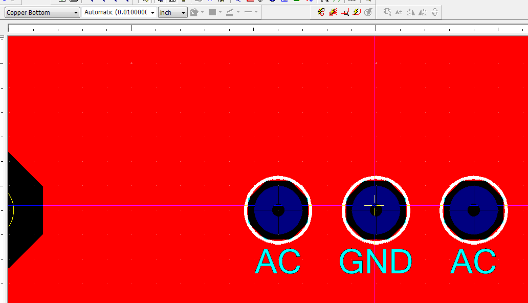
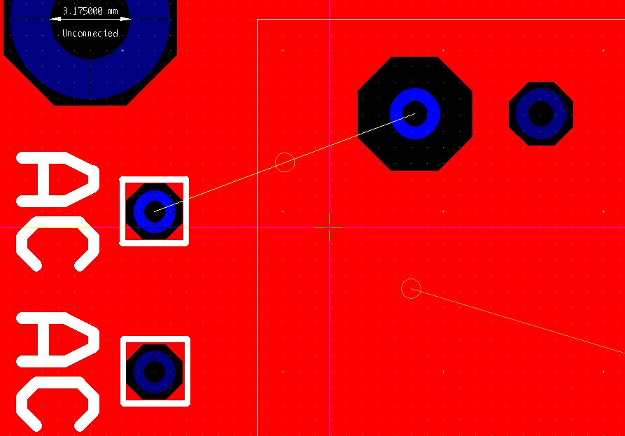
The bottom layer of copper is a ground plan and the two marked holes AC need, according to a chart, 1.25 mm with a value of copper removed around them. I was able to accomplish that for one of the holes of transformer (transformer is the white outline) simply by setting the clearence trace in the net Editor. How to remove the 1.25 mm of copper for the hole in the AC?
(Key AC) properties > General > releases
-
I am using a ground plane with '+' style contact to the parties. With a width of talking to. 010 ", contact the parties in many places is too skinny, but its just for others. This fact prevents me to extend width talks to solve the problem.
I tried to add traces of copper manually, but the plan of mass resists my efforts to redirect the traces or refusing to connect them to the plan altogether.
How can I increase plan connection of parts, without forcing on them?
Thank you very much, Tod
Hi Tod,
Your title and and the question does not seem to match. I answered the question in the main content in difficulty working with the ground plane...
On the question of the Key Edit Layer , Ultiboard lets you set custom stamp shapes, as opposed to the standard circular, rectanglar, forms etc. Creating a new custom cushion form (click on Tools > Database > database manager, then click on the new button in the parts list and select Custom Pad form), will create a document to change the shape of cushion. The document will be a layer, the layer change Pad
-
How to make an object of deep zoom images in 3d
well, looks at this 17 s video (and sorry for the low-res vid x()
theres a film than zoom in / or drone like this video rec
I can understand how to make the text 3d such as 3d tracking
But how do you do (red and yellow) line like that?
Thus, the line as draw in 3d space and have a depth
Thank you
I can understand how to make the text 3d such as 3d tracking
But how do you do (red & yellow) line like that?
Thus, the line as draw in 3d space and have a depth
looking at your specific reference - these seem to be flat lines in 3d space. one way to do, is after you 3d on caterpillars and set your master plan, you can have a change of shape layer the ground plan null parent, add a path and draw in space 3d can open another view to the view of face and personalized your way. in a configuration up like this:


-
Hey guys, im new to AE and I'm having a problem with something and I hope you can help, I do not know what to call it if I had trouble looking for the forums for solution, that is. I have camera followed my images, one of the layers I'm trying a null parent disappears when I pig whisk the properties to the properties of NULL values. the null value is still in place and visible, but the layer I want is now gone. If i a parent the layer it returns. I tried it with a null value and a solid and it does the same thing, I hope it's a cause to retouch its really frustrating me. Thanks in advance
Sounds like a problem of workflow. The procedure is to keep track of the camera, set an origin and ground plan, add a camera and a null value or solid or text. When you get to that point and you want to place a new layer to the same point as the null value, do you this layer 3D layer (which can remove it from the view) then hold down the SHIFT key and parent layer to null. This will break the new 3D layer in the same position, orientation, rotation, and scale as the null value. Once you have done this, you can remove the parenting. Followed by the camera only add data keyframes and orientation to a camera. All layers, text that you add using Camera Tracking and NULL values are positioned in 3D space. They have not committed to animation.
I suggest that you type Camera Tracking in the search help field at the top right of EI and carefully read the help files and then look at some tutorials, so you can figure out how to use this tool in the right way.
-
Hello guys I have had this problem for a while, I want to use 3d etc. texts but I can't I have tried several times and it fails you know all the solutions. ?

First of all, the game of images often have not changes in true perspective so, basically, there is nothing to follow which makes sense.
Second, the hands and the knife in the foreground are important elements which will be the subject of a follow-up, but have nothing to do with the perspective that you are trying to capture and analyze.
Third, your photo is long 30 seconds. From what I've seen screenshots of games, it is hard to imagine that the scene is fairly stable or coherent enough to follow successfully.
To the camera successfully track a shot you must fixed geometry in the scene that matches the geometry in the real world. You must also remove or remove all tracking markers that are attached to things that are in motion in the scene. You should also only executives in the tracks camera shot where you want to insert 3D elements in the scene.
For example, I recently had a shot where a player passed several windows. We needed place 3D elements in 4 different windows. In some cases, there were two windows in the shot at the same time. The solution was to first duplicate the layer of film that cut then the shooting in 4 separate shots which lasted from the first image where a window will appear the last framework. I did this by dividing the layer in AE into 4 pieces and adjusting the entry points and each copy to cover only the part I needed. Each of these layers were composed before and each was recorded separately. They have averaged about 5 or 6 seconds each. In every shot I put the ground plane and the origin, added a camera and a null value, added my items in 3D text and strong support for one of the shots and C4D lite for others. Then I disabled the images of reference in each of the pre comps. Return to the main competition, I had just the 3D elements and the original film so I could complete the composite. This photo would have been impossible or nearly impossible to track in a single pass.
I hope this helps. Without seeing your real shot, I can't offer better suggestions other than to say that it is usually almost impossible to get a good camera trail gameplay if the shot is long more than a few seconds and there are a lot of things happening in the framework. The tool has never been designed to do what I think you are trying to do with it.
-
Need some clarification on decode (AND)
The example that I am referring to comes from DECODE
ORDER_ID CUSTOMER_ID ORDER_STATUS LOCATION RECOGNITION METHOD
2458 101 0.00 postOffice certified Air
2397 102 1.00 warehouse Air certified
2454 103 1.00 warehouse Air certified
2354 104 0.00 postOffice certified Air
2358 105 2.00 ground postOffice certified
2381 106 3.00 ground warehouse certified
2440 107 3.00 ground warehouse certified
2357 108 5.00 warehouse Air assured
2394 109 5.00 warehouse Air assured
2435 144 6,00 secured to the floor of the post office
Assumes that the value of
order_statusis used in the form of bitmap where the first three bits contain information about the order and the other bits are always 0:- The first bit is used for location data:
- 0 = Post Office. This corresponds to the values of 0, 2, 4 and 6.
- 1 = the warehouse. This corresponds to the values of 1, 3, 5 and 7.
- The second bit is used for the method:
- 0 = air. This corresponds to the values of 0, 1, 4 and 5.
- 1 = mass. This corresponds to values of 2, 3, 6 and 7.
- The third bit is used for reception
- 0 = certified. This corresponds to the values of 0, 1, 2 and 3.
- 1 = insured. This corresponds to the values of 4, 5, 6 and 7.
DECODE (BITAND (order_status, 1), 1, 'Warehouse', 'Post office'). DECODE (BITAND (order_status, 2), 2, 'on the ground', 'Plane'): DECODE (BITAND (order_status, 4), 4, 'Assured', 'Certified')
Please explain how know what value to use for the second parameter of the function bitand above? I have seen a few examples up bitand (column 64), bitand (column, 128), bitand (column, 256)
What to do when you have more than 50 different status values? must we first arrive at a setting the time for each of the 50 state values?
DECODE (BITAND (order_status, 1), 1, 'Warehouse', 'Post office'). DECODE (BITAND (order_status, 2), 2, 'on the ground', 'Plane'). DECODE (BITAND (order_status, 4), 4, "Insured", "Certified")
Please explain how know what value to use for the second parameter of the function bitand above? I have seen a few examples up bitand (column 64), bitand (column, 128), bitand (column, 256)
You already have a reference to the answer in your own message:
- The first bit is used for location data:
- 0 = Post Office. This corresponds to the values of 0, 2, 4 and 6.
- 1 = the warehouse. This corresponds to the values of 1, 3, 5 and 7.
- The second bit is used for the method:
- 0 = air. This corresponds to the values of 0, 1, 4 and 5.
- 1 = mass. This corresponds to values of 2, 3, 6 and 7.
- The third bit is used for reception
- 0 = certified. This corresponds to the values of 0, 1, 2 and 3.
- 1 = insured. This corresponds to the values of 4, 5, 6 and 7.
Bits are binary. The 'first bit' is the wick at the right. The rightmost bit, once defined, type has a value of 2 ^ 0 or '1', that's what you use as the second parameter.
The 'second bit' ((deuxieme right), once defined, has a value of 2 ^ 1 or '2' (in binary) If you use '2'.
The 'third bit', once defined, has a value of 2 ^ 2 which is the "4" for you to use 4.
The 'nth bit' has a value of 2 ^(n-1) - so the 5th-bit value is 2 ^ 4 which is 16 so you would use 16.
What to do when you have more than 50 different status values? must we first arrive at a setting the time for each of the 50 state values?
Yep! This small 50th has a value of 2 ^ 49-online 562949953421312
"Warehouse AND on the ground" would be the TWO bits 1 and 2 which is binary 3.
So, if you come to BITAND (order_status, 3):
1. If the est0 or bit value is defined is Post Office AND Air.
2. If the value is 3 the two bits are set is warehouse AND field
You dig a hole for yourself using missions like yours since each bit is used for many things. For example the first bit means, post office and warehouse, depending on whether the bit is defined or not.,.
But what happens if you have three or more 'locations?
- The first bit is used for location data:
- 0 = Post Office. This corresponds to the values of 0, 2, 4 and 6.
- 1 = the warehouse. This corresponds to the values of 1, 3, 5 and 7.
- The second bit is used for the method:
- 0 = air. This corresponds to the values of 0, 1, 4 and 5.
- 1 = mass. This corresponds to values of 2, 3, 6 and 7.
- The third bit is used for reception
- 0 = certified. This corresponds to the values of 0, 1, 2 and 3.
- 1 = insured. This corresponds to the values of 4, 5, 6 and 7.


That makes no sense at all. How can 'Air' correspond to a value of "4", if this value means "Post Office" and "insured"?
You do not want to mix raw values like this.
And it is rarely necessary or enjoy combining several attributes to a single value. A best practice is that each value represents an attribute:
1 location
Bit 1 - Post office
Bit 2 - warehouse
Bit 3 - Garage
Bit 4-...
2. method
Bit 1 - Air
Bit 2 - ground
. . .
But the better question is why is of type bit mapping used at all?
I you LOVE bitmapping and it is extremely powerful when used in a case of correct use. Your use case does not seem appropriate.
Maybe you are looking for
-
I have a W540 which was enchryption at a given time and a person released in the machine image. It has now a ghost boot sector I can't get rid of and need to. I have access to the drive and the PSID, I'm looking for the tool to be able to return this
-
When reading the call of duty - modern warfare II in multiplayer, it blocks on the desktop.
When I reboot I get this message: "ati2dvag display driver has stopped working normally." I've updated my ati driver but he persists. any suggestions?
-
can not find correct for wifi dropouts 'limited access '.
I have an Acer Aspire V5-571P-6642, windows 8, just bought. I can't figure out how to get wifi stop randomly say 'limited access '? It happens a few times per hour, suddenly a page won't load no and if I wait long enough the wifi will say "restricte
-
I just bought a Linksys WRT160N router and the first task to load the program on my main computer has already encountered an obstacle. It says it cannot find a network adapter on my computer and I need to allow. My card work as I am on the net right
-
Signal from the internet my computer losses.
My PC is continuing to lose its signal whenever I play a game then that on internet explore, or when I look at a website of amd. This may be the cause?