LabVIEW FPGA while loop (first call? (VI) question
Hi gentlemen!
I am creating a LabVIEW FPGA VI appearing in a WHILE loop. He has a first call? VI in which, in the first occurrence of the loop, a variable must be initialized to some value. However, when I incorporate the VI in the FPGA, it would seem that the first call? VI has not been called. I also tried this implementation through registers at offset where the registry is initialized outside of the WHILE loop. However, the result is always the same. May I ask how the LabVIEW FPGA functions when it comes to everything IN a loop? Thank you very much!
For some reason that I don't me remember not I avoided the use of FPGA FirstCall and instead, I use a change sign boolean, son of genuine in the terminal, on the left and a fake in the while loop to the right Terminal. As a result, you get a true for the first iteration only, in exactly in the same way that the function of FirstCall. It could even use fewer resources on the FPGA?
Tags: NI Software
Similar Questions
-
Hello
I m using a module NI 9870 in my Crio system and the program worked fine.
The problem I have is that I also need to use a Profinet PN module, and when I try to use both programs included in my FPGA, my 9870 module does not work like it s supposed to (it s points--instead of the characters).
Can someone help me with this? is it assumed that the different loops are independent and without any problem, are - it true?
or do I have to implement a program in a different way?I would appreciate any idea or entry,
Thanks a lot for your help!
Thanks to all for the replies.
I ve already solved the problem, and it was the size of the FIFO for reading.I use only a FIFO for reading, and to do this, I included a number after the data, according to which I m from port to aid. When the size of the data in the FIFO is not exactly the same that in the FPGA program, this function does not work correctly and returns false data.
After this change, the program worked correctly.
Thanks in any case again for your time! -
Two questions in table "While loop"
Hello
I have two questions about creating tables in while loops. I'm using LabView 8.5.1.
In its simplest form, my current while loop (delay set to 0, 2 s) has 3 variables that have been changed by moving a slider. They are each sent to a line in a block of 'Building the table' (data type is DBL 1 d) - this table is then written to a spreadsheet file, such as the three values are written to a new line (one value per column) whenever the while loop runs.
Question 1
How can I add a column 'Time' in this worksheet? In other words, get at the present time the loop works since then, from 0 seconds in the spreadsheet, via the table block building.
I can think of how to do this with a loop For, but given that the While loop runs through an unknown number of iterations, I can't figure out how to get the counter to work.
Question 2
How can I text column headings on the worksheet?
Thanks for the help and if you need anything anyone stating, please let me know

To answer question 1:
There is a function of 'Elapsed Time' you can put as the first colum of the data.
This then reformatted your spreadsheet as
Time Data1 Data2 Data3Time Data1 Data2 Data3
Time Data1 Data2 Data3
etc...

To answer question 2:
Build a table of positions, then write this table in the file only once, outside the loop.
Your table with the data and time will write inside the loop.

-
Is it possible to execute a loop For independently within a while loop in LabVIEW 2013?
In my program, I want to run a loop For inside a while loop and run independently, at their own rate of execution. A test, I wrote a simple VI with a while loop with 1 second calendar and in this I inserted a loop For with 3 of a second. I created indicators for the two terminals of the iteration. When executing the VI, I found the while loop waiting for loop For run N times before the while loop is executed again. I also found that sometimes the first iteration of the loop For ends at 1 second instead of 3 seconds and the STOP button to complete execution of the While loop does not always work.
This is the expected behavior. LabVIEW is the language of s DATA stream. If you want the curls to be independent, it can be data forcing addictive so use separate loops.
-
Using asynchronous calls in a while loop. How 'Skip' node and only retrieve data as it is treated
Maybe I'm not understand asynchronous calls... but I thought I should be able to call one another VI and essentially 'jump' it is the node and only receive data as the called VI treats. In other words, similar to the Run of VI, I can wire a wait until done? with a fake and the main VI will not wait for the other VI end of race. The main VI continues to function, and when it passes the called node of the VI, it will receive data if it happens to be there.
How can I call a VI in a while loop and do not wait so he could spit out the results? Data flow is my enemy on this one...
The first VI treats its own figures (using the iteration count) and displays them on the PC. Other indicators are the data of the called VI. I want to be able to work around the blue circle node and receive data only that it will be available.
Any help is appreciated. Thank you.
What I said OR the 'Start asynchronous call' is the preferred method for starting background tasks. This call is usually used to run background tasks. For example, you have a process of journal. When your application starts it would use the "asynchronous call Start" to start the process of journal and then move on to the other stuf. The process of the journal would then happily run in the background and the main application is free to do other things. Of course when implementing these types of systems you need a way to coordinate things like exit. This is where the queues and stuff come it.
-
While loop with stop unwired FPGA button?
I've seen examples FPGA with a while loop where nothing is plugged to the stop button. On a target PC, it would throw an error. What it means?
I think you are talking about "Timed loops" that are "single-Cycle timed loops" on FPGA.
FPGA is intended to be run until it is powered, a 'Stop' software does not much sense.
Norbert
-
bbmChatDB of public database;
public static FileConnection fconnRead = null;
public static String fileReadData = "";
public static InputStream is = null;
data Byte [] = null;
DataInputStream is = null;Here is my code...
I have 3 files in my directory... When I run the code I can open a file and read it... but the while loop get blocked after the first iteration... can someone me help or give some indications
try {}
FileConnection fc = Connector.open("file:///store/home/user/documents/BSM/") (FileConnection); "
If (fc.exists ()) {}
Enumeration e = fc.list ();
While (e.hasMoreElements ()) {}
System.out.println ("files are:" + (String) e.nextElement ());
play this file
StringBuffer stringBuff = new StringBuffer();
try {}
System.out.println ("opening file")-;
System.out.println ("file name is:" + (String) e.nextElement ());
fconnRead = Connector.open("file:///store/home/user/documents/BSM/(String)e.nextElement(),Connector.READ_WRITE) (FileConnection);
System.out.println ("data length")-;
If (fconnRead.exists ()) {}
is = fconnRead.openDataInputStream ();
data = IOUtilities.streamToBytes (is);
Ddd = new String string (data);
fileReadData = ddd.toString ();
System.out.println ("length of data:" + fileReadData.length ());
System.out.println ("read data :" + fileReadData);}
} catch (IOException ee) {}
ee.printStackTrace ();
System.out.println ("Exception in the read data :")
+ ee.getMessage ());
}}
}} catch (IOException e) {}
e.printStackTrace ();
}{Finally
try {}
If (is! = null) {}
is. Close();
}
System.out.println ("is closed...");
} catch (IOException e1) {}E1. PrintStackTrace();
}If (fconnRead! = null) {}
try {}
fconnRead.close ();
} catch (Exception e) {}
System.out.println (try ());
}}
}
You can recode this treatment so that it uses only:
e.nextElement ())
Once a loop iteration.
Directly at the start saying something like:
String fileName = e.nextElement ());
and use fileName everywhere in your loop.
Also be aware that printStackTrace() will do nothing in your situation, it only works if you catch Throwable. So make sure you something output all your catches exception and also have a catch (Throwable t) to catch the things you miss, as follows:
{} catch (Throwable t)
t.printStackTrace ();
System.out.println ("Eception exception:" + t.toString ());
}
I think your code is thrown an exception and you don't see it.
-
My program is complete in a while loop. Once it runs, it will use kinect to keep my data of position of the head, so it will generate a position once. I want to reach 5 positions and can calculate 3 speed and acceleration 2. How can I get 5 times while it generates 1 time?
If your data are made at the edge of the while loop and you right-click where the wire exits the while loop, you can select "Enable Indexing" that will produce a table of the data received as large as the number of times in the loop. You can also check the "examples: help find ' ' Producer/consumer', which will allow your receiver (producer) loop to get the data and send it to a processing loop (consumer).
-
Question for LabVIEW FPGA DRAM
Hi all
How can I correctly address the 128 - bit DRAM memory? I have the Bank DRAM 0 set as a memory of 128 bits, set up in my design as a CLIP. I realize it's a wide RAM on 32-bit. I had a National Instruments AE do the original design I've been adding to. He said that the addresses needed to incrementing by four with each entry. Example: if I had to write in consecutive addresses, I would write to the address: 0, 3, 7, 11, 15 etc, and I would like to send 128 bits to each address. My address is calculated as: (number of pixels in a line of video + line * (number of pixels per line) for a picture of the video). So I take my calculated address and add 4.
However, I checked an example in the finder example: example of integrity hardware flexRIO/IO/external memory/memory. In this example, 128-bit data is sent to the memory and the address is incremented by 1 (instead of 4) each cycle clock as valid data.
Who is this? Section of the help for this function is ambiguous.
Sets the address in external memory for reading or writing. The physical data bus for external memory is 32 bits wide (4 bytes). Each unique address value represents 4 bytes of data. Therefore, the total number of unique addresses in external memory is equal to (Memory Size in bytes)/4.

Note  The memory interface exposed to LabVIEW FPGA is 128 bits wide. As a result, each memory write or read operation accesses four different address locations in memory. The memory controller latches this signal value only when you issue a new memory write command by asserting the Command_Write_Enable signal.
I'm confused by the 2nd paragraph "every Scripture memory or read operation four access address locations of memory." Does that mean I increment the address by 1 to get 128 consecutive bits 'locations' (Yes, I know, that's 4 words of 32 bits in memory), or do I increment the address by 4, in the order of words of 32 bits 4 by 128-bit single transfer?
Thanks for your help.
-J
Hello J,
I want to clarify my previous post. There are two ways to access memory DRAM, CLIP (that you have described is what you do) and using the memory node. As noted before, the DRAM is 128 bits wide. When you write to the CLIP you basically write pieces that is the width of the databus (in this case 32-bit). Therefore, when you write a total of 128-bit DRAM, you place 32 bits in each address. The address being the width of the databus, then you write with a writing & the address 0, 1, 2, 3. Then the next write will be 4, 5, 6, & 7 and then address 8, 9, 10, & 11 and so on. In this case, you must increment your address by 4 whenever you write. Note that you start at 0, then 4, then 8, etc 12. In your previous post, you were out of a figure.
There is also another way to write in the DRAM memory, and it is through the node of memory, which is what is used in the example that you are pointing out. Here, LabVIEW takes on some of the thought, and instead of being the width of the databus address, they are the width of the entire segment of 128 bits. So when you write to DRAM here, you only increment 1 whenever address because they refer to any segment of memory. This contrast with the CLIP, address 0 of the memory node interface match the addresses 0, 1, 2, 3 in CLIP mode & and address 1 of the memory node would correspond to 4, 5, 6, 7 in CLIP mode addresses &. If you do not write an integer of 128 bits for the memory node, then the remaining addresses in the data block are filled with "junk" so that the address remains constant.
As I mentioned previously, it is the most effective writing in chucks of 128 bits so that you don't waste all of the DRAM. I hope you find this explanation clearer.
Brandon Treece
Technical sales engineer
National Instruments
-
Use of LabView delay in a while loop instead of use the inherent instrument of time loop.
I have a lmg500 sez I use. It has the possibility of continuous measurement of data, with a cycle of user control loop (always using a while loop but the delay comes from the instrument). The problem is that the time of the loop is not constant. Can I use a very short time (100ms) as the cycle of the instrument of the time, but use a longer period in time loop collect data?
I know that many instrument offers the same capabilities, so the issue is relevant to each of them.
Thanks for any help
You're not going to be accurate with Windows. The time between samples should be that you have programmed the instrument (i.e. the time between each value in the table 1 d) but the rate of the iteration of a while loop always will be the subject of a jig on a bone not real-time.
-
Model a block synchronous dual-port RAM with LabVIEW FPGA
This question caught my attention recently.
I am trying to model a particular design element called "RAMB4_S8_S8" with the LabVIEW FPGA module. This element is a block synchronous dual-port RAM allowing simultaneous access to two ports independently from each other. That being said, a port can perform read/write operation to this RAM while at the same time, the other port might be able to do the same thing. There are two opportunities of possible port conflict, however. The first is when both ports are trying to write to the same memory cell. The other scenario is when a port writes in a cell memory while at the same time the other port reads from it. Other than that, everything should be a legitimate operation.
In order to reproduce this I select memory block that is integrated into my FPGA target. An interface is configured to be the playback mode, and the other is set to write fashion. For the option of arbitration, I let the two interfaces to be "arbitrate if several applicants only. Then I got a compiler error when I tried to run my FPGA code for this model in a SCTL. The error message is something like "several objects to request access to a resource through a resource configured with option interface" arbitrate if several applicants only ", which is supported only in the single-cycle Timed loop if there is only a single applicant by interface.
This error goes away if I replace the SCTL with a simple while loop, but not what I would like to implement. So I wonder if there is a better solution to this problem, or is it just the limitation of the LabVIEW FPGA module.
Thank you.
Yes, you can use a form of conduct to perform the operations you want in the generations clock cycles, but all the code is inside a single SCTL. Basically, read the first address and storing in a register in a single cycle and then read the second address in the second clock cycle. This would allow you to two readings of valid memory every clock cycle 2. I have included a crude extract to illustrate the concept. The case selectors are identical with address A being connected to the memory in the true case, B in the case of fake address. Your biggest model memory dual port will be intact, but it will operate at 1/2 rate.
Take a look at the white paper that provides more details on the construction of memory:
Data on a target FPGAS (FPGA Module)
The ball on the memory block indicates that memory block double port cannot be applied in a configuration of reading, which is a double ROM. access read/write port must be imitated with custom code.
-
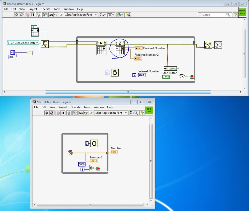
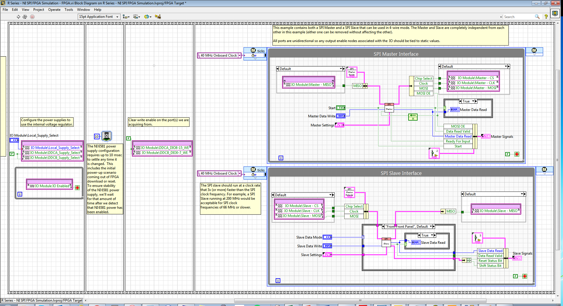
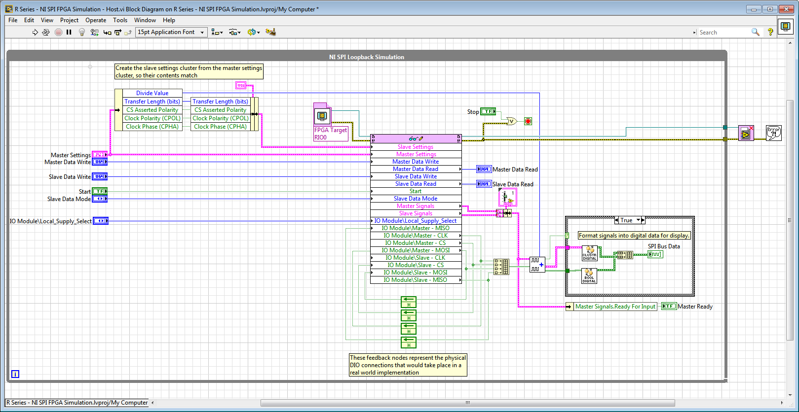
LabVIEW FPGA SPI accident - SPI OR IP address for example - R series OR
Hello
I am trying to run the series R - sample project NI SPI FPGA Simulation.lvproj that comes with the SPI IP OR on a real FlexRIO FPGA SMU-7976R target with an attached digital adaptation NI 6581 B Module. The example is for a PCIe-7841R but I wore during my target FPGA, follow these steps and made additional changes to try to make it work with my set-up. I learned that FlexRIO FAMs CLIPs do not work with nodes in office had so I know I can't simulate the project originally planned so I will try to use FPGA to e/s node host side (open FPGA vi reference) to implement the actual hardware.
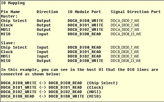
My first question concerns my configuration of the adapter module e/s and selection. I added the IO Module (NI 6581 B: NI 6581 B channel) for my project and selected the channels as shown in the table below. I have a real physical hardware connection as described below using two NI SHC68-C68-D4 cables and a break-out Board.
I changed the names as well:
I selected these DIO channels because I wanted the DDCA connector to be the master and the DDCB connector to be the slave. In addition, in this CLIP every eight channels of i/o has a write enable signal. I have not used the Port configuration because I needed 4 available DIO channels and I saw DIO0-3. Is my logic of selection of channel vs correct Port here?
Following the same strategy that examples FlexRIO/NI6581B, I changed the FPGA.vi to include initialization outside of timed loops:
And in the Host.vi I have a node reference FPGA and wired loops of feedback accordingly:
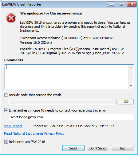
When I compile the FPGA and try to run Host.vi LabVIEW inevitably crashes with Crash Reporter below and must restart:
Does anyone know what I'm doing wrong here? My guess is that it has something to do with the CLIP/IOModule. Any help is appreciated.
Thank you
Scott
Hi Scott,.
I suspect that the problem might be related to the fact that your node open FPGA VI reference is in the while loop and trying to open a new FPGA reference at each iteration.
If you move outside of the while loop, it does not solve the crash?On channel vs port question, your logic seems reasonable to me, but I recommend to try it since this feature could depend on device.
-
Control and Simulation in a loop / while loop with TCP/IP reading / writing of synchronization
Hello, I have a problem with reading TCP/IP and written in two loops. The problem is NOT to get the two loops to read and write to and from the other. This has been accomplished. My problem is when I run control and the loop simulation on my laptop and the while on a RTOS remote on the controller on-Board of LabVIEW in a remote PXI chassis, the while loop the remote system running on four 4 times faster than the loop control and simulation on my laptop. In other words, for each iteration of the loop control and simulation on my laptop, there are 4 four iterations of the while loop on the remote system. I need to know how to get a degree of kinship (1:1) with these iterations of the loop. When I run a longer simulation in real time, say 10 seconds, the control and Simulation loop begins to slow, i.e. the simulation time slows down until it is no longer in real time and the "Late Finish"? Parameter is set to true and the LED lights and continues to stay lit. At this point, the system destabilizes due to what I believe is being well sampling rate too discreet and I have to end the simulation. How can I get a ratio of one to one between the loops and also to avoid slowing the loops causing destabilization?
To give an overview of my application, I implement a control system in a network, seen in "image2.png". This is achieved using my laptop as a subsystem 1. Reference signals are generated from the laptop and the error signal is produced. Control measures taken and the control signals are sent via TCP/IP to the remote system. Position feedback is returned, and the process repeats. My system has Core I7 Procs w / 3 GB of RAM, up to 1 GB/s speed via ethernet and LabVIEW 2011 installed with all necessary modules and networking tools. The attached VI Custom_Wireless_Controller works on my laptop. The remote system I'm working on that has the 7830 NI R Series with FPGA card. OTN runs on the PXI chassis with an enbedded controller that has networking capabilities of up to 100 MB/s via ethernet. I use the FPGA for the acquisition of data and apply control signals to my plant. The plant is the PCE twist connected to the FPGA through the cable of the ECP - RIO of NOR. Subsystem 2 is this side of the CNE. The FPGA collects position, he sends to the controller via the network, receives signals from the network drive and writes signals to the plant power amplifier that operates the plant. This process is repeated and the VI and is titled Custom_Wireless_Plant.
I appreciate the help really and look forward for her and for any question!
Well, the first step is to understand what you have set up right now. Your control and Simulation loop on the side of the controller is configured as 'Runga Kutta 4' and you have a loop timed on the other side. In addition, you have the primitives of TCP/IP on the control and the Simulation diagram and means he will perform (a message) on the size of each minor step, which in your case is 4.
So, you have two options:
1. replace the Solver side controller Runga Kutta 1 (this must synchronize loops)
2. hold RK 4, but create a Subvi around two primitives of TCP/IP and configure from the VI to run than the major (continuous) step-size. If you do it right, you should see a 'C' on the upper right part of the VI you have created.
Please let me know if what I said is not clear...
-
LabVIEW FPGA: Integration node clock wrong
Hello
I'm having some difficulties to understand how the clock is part of the node IP for LabVIEW FPGA and was hoping to get some advice.
What I try to do is to set up a digital logic circuit with a MUX feeding a parallel 8-bit shift register. I created the schema for this Xilinx ISE 12.4, put in place and can't seem to import the HDL code into an intellectual property node. When I run the VI, I am able to choose between the two entries for the MUX, load the output in the shift register, clearly the shift register and activate the CE.
My problem is that when I switch to the entrance of THIS, he should start 1 sec shift (Boolean true, SCR, High, what-have-you) in the registry once each clock period. Unfortunately, it instantly makes all 8 bits 1 s. I suspect it's a question of clock and here are some of the things I've tried:
-Specify the input clock while going through the process of configuring IP nodes.
-Adding an FPGA clock Constant as the timed loop.
-Remove the timed loop and just specifying the clock input (I'm not able to run the VI that I get an error that calls for a timed loop)
-Do not specify the clock to enter the Configuration of the IP node and wiring of the FPGA clock Constant to the clock input (I can't because the entry is generated as a Boolean).
-Remove an earlier version of the EC who had two entries up to a door and at ISE.
-Specify the CE in the process Configuration of the IP nodes.
-Not specify this in the process of setting up nodes IP and wiring it sperately.
-Various reconfigurations of the same thing that I don't remember.
I think I'm doing something wrong with the clock, and that's the problem I have. Previously, when I asked questions to the Board of Directors on the importation of ISE code in LabVIEW FPGA, a clock signal is not necessary and they advised me to just use a timed loop. Now, I need to use it but am unable to find an explanation online, as it is a node of intellectual property.
Any advice would be greatly appreciated, I'm working on a project that will require an understanding how to operate clocks the crux of intellectual property.
Thanks in advance,
Yusif Nurizade
P.S. I have attached my schematic ISE and the LabVIEW project with one of the incarnations of the VI. The site allow me to add as an attachment .vhd file, but if it would help I could just paste the body of the code VDHL so just let me know.
Hello Françoise,.
I spoke to the engineer OR this topic and it seems that it was sufficient to verify that your code works, by putting a wait function of 500 ms on the while loop to check that the registers responsible and clear. I'm glad that it worked very well!
-
Subvi with while loop + event structure works is not in multi tab VI
Hi all
I'm developing an interface for the control of a prober using Labview 2012, and I'm stuck with a question.
First I provide you with a simplified version of my VI control interface and the sub - VI used to generate and manage the mappings of wafer.
The VI is composed of several tabs: Prober initialization, manipulation of Wafer, Wafer map, status, error.
The sub - VI can:
1 / initialize the grid to display the map (Subvi Init grid not provided here)
2 / coordinates XY for import a txt file (Subvi Wafer map Import)
3 / view contact information and the index of the sector under the cursor
4 / and what position die is double clicked and the Boolean 'Edit Wafer map' is true, then the user can change the State (color) of the matrix between die on platelets and selected Die
My question:
If I use the sub - VI by itself, it works fine. However, when I use it as a Subvi in the 'Wafer map' tab, the plan does not rise and I can use any features incorporated into the Subvi.
I suspect that the while loop + structure of the event of sub - VI the bottleneck here.
However I do not know which way to go, that's why I'd be happy to have some advice and help here.
Thank you.
Florian
The question arises because your hand loop 'for' cycles of 33 times. In the loop of 32, appears your Subvi and execution is passed to your Subvi. During this time your main VI expected Subvi in the end, she never does. You could spend your Subvi out of the main loop of the program and run in a separate process, in order to pass data using queues, but you have to find a way to close the Subvi (i.e. a queue). By moving the Subvi on the main process, it is independent and you can do what you want to do with the events and others.

Maybe you are looking for
-
How can I see what I have stored in iCloud?
How can I see what I have saved in my different devices iCloud?
-
Custom generated changes shape when sent to the compressor
When I send my project to compressor (file... Send to compressor), a custom shape that I generated exchange of positions on the screen. This occurs in two places. In other words, everything is as it should be when in FCPX. When I sent it to the co
-
Satellite A500-02J001 - Intermittent TV Tuner?
I recently bought a new laptop Satellite A500-02J001, running Windows 7 Home Premium (64-bit). I have properly configured the integrated digital TV tuner, analysis 28 channels with Windows Media Center. But the next time I went to use the TV tuner, W
-
TMP files automatically open with
I clicked the always open this type of file with the function 'open with' option to open a TMP file created by my Canon ZoomBrowser and now I can't stop all the TMP files to open in my desktop photo manager. How to stop?
-
my system does not start upwards - don't stop progression blue bar that goes round and round. I can boot into safe mode and safe mode with networking mode.