The initialization of the BRAM on FPGA
Hey guys,.
I have a small question. In my properties BRAM, I put the initial values to 0. But if I write a FPGA code where I just read the first 11 addresses in my BRAM there are only those inside the BRAM.
After that, I fill the BRAM by others because I want to check under what conditions the BRAM is reset to its initial values again.
As I said, there are already in the BRAM even if I run this bitfile for the first time (VI could not start after compilation because of a difference between the VI and bitfile).
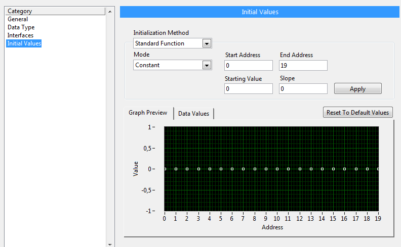
So what LabVIEW sets the initial values of BRAM?
Hey Jon,
Thanks for your effort. I just tried another approach. Now, I use two bitfiles. A first for the initialization of block RAM, and second for the program. So in the first one that I write zeros in the ram block. These seem to be saved or at less the self initializing works... I don't like as long as the RAM block is filled with zeros when I start my main application
Kind regards
Slev1n
Tags: NI Software
Similar Questions
-
USRP RuntimeError: Please update the firmware and FPGA images for your device.
Hello
I have an Ettus USRP N210 with a surfboard RF WBX running FPGA firmware version 4.
2009 LabVIEW and NOR-USRP 1.1
When I try to run one of the USRP VI OR as devices to find it displays the following error code:-1074118627
"niUSRP Devices.vi find
a length or configuration error has occurred."
Code: 1440
Details: RuntimeError:
Please update the firmware and FPGA images for your device.
See application for USRP2/N-Series notes for instructions.
Compatibility of the Protocol expected number [7-11], but received 12:
The version of the firmware is not compatible with the host code generation. »I can communicate with unity on Linux using UHD machine and the utility Configuration NI USRP can see the device, but firmware update is not possible, probably because of my IP ending in 221. Latest firmware Ettus was recharged via Linux UHD.
Looks like my firmware again? I am not allowed to download the old versions of the FPGA firmware.
Can someone help me with this problem please?
With respect,
-Sigurd has.
Hello Sigurd,
The NOR-USRP driver requires a specific firmware and FPGA image to be downloaded to the USRP to exploit.
You can use the utility of Configuration USRP download appropriate firmware and FPGA image to the usrp.
This knowledge base article will help you: how update the Firmware and FPGAS Images for N2xx and NI 292 x USRP
-
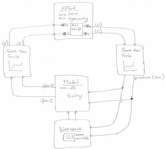
Impose a factor of scale between the model and FPGA
Hi all
I have a VS project configuration that unfolds on a real-time system. The project has an FPGA and a model. Some of the output of the cards of the OD of the FPGA model. In addition, some of the AI of the FPGA cards at the entrances to the model. Here's my problem. The AI FPGA gives me a measure of voltage, but the model takes only a pressure (bar) as input. This means that I need to convert my blood pressure using a table or a formula. How to make that happen?
Also, I want to use the same lvbitx FPGA and the same model of dll on various physical parameters. The only difference between these physical configurations is the forumla/table (for example, a different pressure sensor is used). Is a convinient way to say VS use different table games?
Hi oeua.uoeuau,
If you have a formula to convert the voltage in pressure, you can use a calculated string to implement. You just point to the computed in your Channel FPGA output and the inport of your model to the computed string. If you need a table of choice, you can create a model of LabVIEW that takes blood and uses a lookup table to get the pressure reading and the outport of LabVIEW model port in the inport else your model.
To switch between the different scallings, you can simply use a procedure to set a variable to be an entry or another.
See you soon,.
< brian="" a="" |="" national="" instruments="" |="" applications="" engineering="">
-
How can I get the Coefficients of scaling for the Butterworth filter FPGA version
I am trying to program a FPGA application where I need to be able to change the cutoff frequency of the filter. I see that I can do a terminal for the coefficients of the filter on the VI express Butterworth filter, but how to generate the coefficients of different cut-off frequencies of filter? When I use the VI of Coefficients of Butterworth host-side small floating-point values rather than the large fixed point values I see on the side turns FPGAS.
Thank you
David R. Asher
Hi David,
8.5 or 8.6, there is an example of navigation that contains the Subvi design filter you need:
examples\R Series\FPGA Fundamentals\Analysis and Control\Filter and filter Butterworth Reconfigurable DC-RMS\Using-R - series.lvproj
In LabVIEW 2009, there is a new palette in my computer: Interface FPGA > scaling, with a new VI of Coefficients of Butterworth on this subject. Who will produce the coefficients quantified, you need in the format expected by the FPGA Butterworth filter.
Kind regards
Jim
-
The initialization of the lut for FPGA
I am currently generate a waveform on an FPGA using a program to initialize a look-up Table (LUT). When I select call VI of initialization, and then select the path and click OK, Labview begins to consume a lot of time CPU, but nothing seems to happen--none of the buttons except the open dialog box file and the close icon (red box with an x in the upper right corner) is grayed out. Someone at - it ideas? Maybe I'm doing something wrong, but there is very little documentation on this function. I have attached the VI that I use to try to initialize my table.
Any thoughts would be great.
Cheers, Matt
This must have something to do with the complexity of the LUT VI initialization. As a work around, I simply wrote the data in a file that I then read for the initialization of LUT. I have attached the screws again.
The lack of reactivity is a problem, but also the absence of any indication of an error.
-
Initialization of the DRAM in FPGA
To test my FPGA (FlexRIO 7966), I tried to test the error trapping. Generally, the error would be caused by an overflow in the FIFO of DMA process (EX: host VI is not reading fast enough causing the FPGA DMA fifo fill then causing my DRAM FIFOs to fill). When this happens, simply reload the bitfile does not seem to clear the condition. The memory is still in the complete state. Even restart the controller does not seem to clear the error. Electric bike does not work, but it's no possible to retrieve errors.
It is impossible to probe whose memory is in trouble, so I ask:
1. when the bitfile is loaded and running, the DMA FIFO is reset? What of the DRAM (configured as FIFO)? Or General FPGA FIFO memory (Blockram, registers, etc.)?
2. it would be of no use to manually clear the DRAM during the initialization of the FPGA (EX: switch from data_available to read in a SCTL initialization until data_available is set to false and ignore the actual data)?
File guides and aid users are very light on works the initialization of FPGA.
Thank you
xl600
-
Disable the extended FIFO FPGA target during execution
Hello
I use a FIFO extended target in my FPGA to constantly calculate the derivative of a measured value (dB/dt). Thus the FIFO stores all values during time dt. This means dt determines the number of items in the FIFO and dB is determined by the actual value less the oldest value in the FIFO. It works well when I initialize with the code in figure InitFIFO.
But the FIFO of compensation is not possible (see figure clearFIFO). In the while loop if "reset dB" is false, as the new value of B is written on the FIFO, then the oldest value is read from, for the number of items in the FIFO remain constant. To change dt during execution, I need to clear the FIFO and initialize it with a new length (number of items). I tried the next loop, but it does not work. The FIFO does not initilized with the elements. The length is zero and the loop counter for (#deltaB Length2) is 0.
What I am doing wrong? Is there a better way to erase a FIFO during execution in the FPGA? I'm now stuck for 2 days with this problem and looking forward to any idea or suggestion.
Thank you very much. Best regards
Andy
Hej,
Thank you for your response. You were correct, that deltab FIFO length was 0 because the defalt value was zero. The problem is that in my host vi on the RT system I put DeltaB FIFO length in a loop of high priority and as you can see when I restart the FPGA, DeltaB FIFO length has a valid value (the code in figure 1 works well with a local variable of DeltaB FIFO length in the FPGA). But the variable to set the variable "reset dB" is under the control of the loop of low priority of the host vi. And there, I had an entry DeltaB FIFO length unwired.
So, I learned that a control FPGA read/write unwired sends a '0' or resets the variable to its default value in the FPGA. I assumed that nothing is transferred and the last variable is retained if you let a control read/write unwired. Now, I learned of this stupid error!
Thanks a lot again!
Andy
-
Possible to use the main clock FPGA as a basic Source of time for the NI 9234?
Hello
I am running a NI 9234, and NI 9222 module on a cRIO-9114 chassis with a real-time 9022 controller, data acquisition on the 8 channels on the full sample rate, using the FPGA.
My problem is the synchronization of the data, where the NI9234 is usually a late acquisition, compared to the NI9222. I tried manually delay the NI9222 to take the first samples, but so far without success.
To solve this problem and also to ensure a rate of data more comparable on both cards, I was wondering is it possible to create a Source of time Base master for the NI9234 WITH THE FPGA (opposite to import from another NI9234 or similar module)? The NI9222 I already provide with sampling of the impulses from the FPGA (as expected with this module).
Another issue would be the characteristics of the exact chronology of the two modules, including in terms of synchronization between the beginning of the acquisition and the first samples of data. I couldn't find any information about it...
Thank you in advance,
O Hoppe
Hello!
I've never heard of a possibility to use a time base FPGA with a module of Delta-Sigma.
But I think that the question should be what has not worked to delay the signal and how you did it. Have you read this article?
How can I compensate for delays of different group with the C Series Modules in LabVIEW FPGA?
http://digital.NI.com/public.nsf/allkb/74EB238E1BCADD528625735300681A7DCan you give a more detailed description of your trial to delay acquisitions? Can you provide a code example?
Best regards
Christoph
-
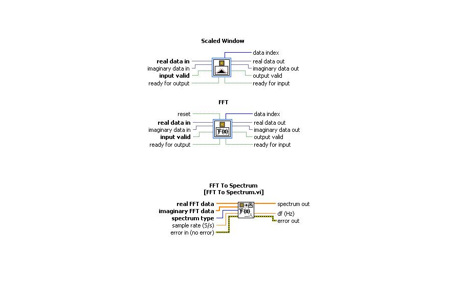
Using the Interface of FPGA functions palette
Hello
I use the card PCI-5640R and PXI-5600. I want to use the "scale" and "FFT" exspress screws to the range of functions 'Mathematical FPGA and analysis' in my VI "FPGA VI" and "FFT spectrum for '"FPGA interface"in my"host VI.
A poster of the code examples in which these three subVIs are used can.
Thanks in advance.
Kind regards
Rashid
The answer to this question is available to
-
basictx & rx in a 310 x cards will do the processing on the side of fpga in lvfpga?
I know you can do host treatment aside with the 310 X + BasicRX/TX routing (thanks to Sarah_Y). But what a FPGA side treatment (with LVFPGA)? Anyone here tried it?
I was wrong. Example of Sarah_Y has an fpga vi and a host vi to interact with him. I had to dig into the usrp library and disable error checking which relates to the number of part of daughter card, but after that it works fine. I (finally) my loopback.
-
How to replace the factory supplied FPGA functionality in myRIO?
Hello
I have created an example of FPGA code and downloaded in myRIO. I expect he would have erased the FPGA factory feature shipped which included all the interpretation of the digital (DIO) of input/output PWM asynchronous universal receivers/transmitters (UART), inputs of encoder, I2C and SPI. Is it possible to put this factory shipped to FPGA code? Where can I get this code?
Thank you
Ajay.
Hello Ajay,
When you run your host code, which calls the FPGA VI (opens its reference), it automatically deploys the FPGA code to the material. If you run after code samples, to come with drivers myRIO, it will deploy default FPGA code included.
To find the FPGA defalt code, which comes with the drivers, create a new project to create a project of-> models-> myRIO and select myRIO custom FPGA project, you will find a FPGA Default.vi of hand inside.
It is sufficient to note that functiality UART is not implemented on the FPGA, but instead uses a feature included in the architecting processor. If you still have the UART functionality, even with your custom running FPGA code.
Thank you
AREV
-
Hello!
I'm in the quest to replace some aging PCI-5640R. I am currently using as a portable-Journal data solution, mounted in a Magma Expresscard to PCI box with a laptop. As a reference of the time, I use a Symmetricom XLi.
The equipment is dependent on the sampling finished a set of samples once a trigger signal goes high and also receive antenna azimuth information using two lines PFI more. The signal is sampled at IF, 30 MHz, and the signal is less than 5 MHz bandwidth.
Now, I started watching the Ettus X 301 with a GPS OCXO and MXI-express interface which should be the same as the USRP-295xR NI. It is available as device NI RIO with three different front ends, unfortunately, none of them work at 30 MHz.
Q-1: Ettus has the front-end 'BasicRX', but it is only considered compatible with LabVIEW driver and not necessarily with the RIO. Is the front-end BasicRX usable with the USRP - 295XR RIO and MXI-interface with LabVIEW FPGA? Should I just avoid trying tune the nonexistent LO? As long as he gives me data, I can live with some error messages during the Setup...
It's the best solution for me, but if it is absolutely impossible, I have a few questions:
Q-2: information on the front end are really rare in the pages Web OR both Ettus, but the WBX is listed up to 50 MHz frequency, to have a filter of low pass of bandwidth of 40 MHz to I and Q. This should mean a total of 80 MHz of bandwidth with I and combined Q,-40 to 40 MHz. Why did the bandwidth to Web pages as OR listed being "40 MHz bandwidth in real time", if the low pass filter of the WBX is 40 MHz in I and Q? Not the band total bandwidth or 80 MHz?
Q-3: assuming a bandwidth-40 to 40 MHz: could I put the WBX LO at 50 MHz, be tuned to the frequencies from 30 MHz to 20 MHz signal,-20 MHz and use a bandpass filter to the FPGA to extract the new signals and remove all other signals?
Q 4: I tried to start a FPGA project in LabVIEW and add the x 301/294xR/295xR as a target. Data clock is locked to 120 MHz, which I guess means he will receive no data to 120MS/s IQ? The x 301 Ettus is listed as provide data of the ADC to the FPGA at a rate of 200 ms/s, could someone explain to me why, OR USRP RIO expects only database 120MS/s?
Hi Idar,
Yes, you should be able to put the basics on your X 310/USRP RIO and use LabVIEW FPGA to receive 120 MECH. / s of the DACs. The example I posted is in fact not for the precompiled file bit. The example I posted is for LabVIEW FPGA, which allows you to add the IP address for the FPGA. There is a sample project that comes with LabVIEW FPGA which is the recommended starting point to build your FPGA application. The sample project has all the configuration set up as well as broadcast continuously and pads/FIFOs in the FPGA and examples for synchronization. There are comments in the code example that show where he must add your own blocks of property intellectual as a filter and decimater you mentioned. The PDF I posted shows what changes you must make to this sample project using the Remora Basic/LF.
I would like to know if I'm not explaining this clearly, or if you have any questions, I'd be happy to help you!
-
FPGA: unable to update the timer on fpga through host.
Hi all
I worked on FPGA project. It has several loops paralel and works with some sampling time.
I would like to change the "timing" on a single loop, it is called loop output. I would like to slow down the loop so that the loop will update the output less frequently. (see attachment - red circle)
I modified the code by changing the timer by the host. (see attachment - blue circle).
I did several things such as:
1. Add a manual switch that allows me to change the time of sampling mode normal (same time of polling with other loops) in manual mode (set the timer number).
But it did not work all the time. I checked the value on the host, it is always on the same sampling time, even I write the value of the timer to measure.
2. I changed the strategy by putting the other control connected directly to the timer (without switch) in the loop so that I can change the value directly. However, there is still no luck. The result is not reliable. It sometimes slows down and many are in the same pace as before.
3. I even put a case in front of the exit structure so it was only updated after sometimes (all 100 or more loops). It is not always useful. I see the speed varies, but it is not as expected.
The material is piezo readers/engine. But I want to slow down the speed, does not increase the speed. Thus, it should not be a problem.
I really appreciate if there are any comments or suggestions.
Kind regards
Areku
Hi all
After consulting with my supervisor, he advised me to spend on intermediate or new control value first. Then, update the value of the control that is connected to the timer loop with this intermediate control value. It will update the value of the timer loop after loop (when intermediary value received from the host and update control connected to the timer loop). It works fine now.
I don't know exactly the mechanism labview of drafting or updating the fpga through host value. But, it seems to me, in my case, there was a problem of writing a value to the control that is connected to the loop timer where ran in relatively fast. Well, little control ignore/reject the new value because it is busy to execute the loop in high speed.
Thanks again for the response to my post, GerdW.
Kind regards
Areku
-
What is the use of FPGAS and how it differs from the IO Modules
Hi all
Maybe it's a silly question for most of you. But I have very less knowledge about the basic concepts of electronic (FPGA, real-time) to cRIOs. I know that FPGA
can be used to generate circuits within the chip that helps by some logical functions.
I've just started working in the cRIO. My question is that we have Modules e/s making it outputs all the application entry. So, what is the purpose of e/s in the FPGA.
Lets consider that we entered for an application of RTD. In this case the module NI 9217 itself exits 24 bits of data from the RTD measurement which may be the process of the LabVIEW VI. What will be this FPGA between the i/o Modules and the processor will help in? Also I want to know what type of communication is used to send data between the FPGA and host modules.
Thanks in advance
Ajay HI:
Sorry, you do not have an answer to your original question. However, you are right about the benefits of the FPGA. You said, if you build pre-processing in the FPGA, you can unload a lot of potentially CPU calculations out of the host processor. In addition, the program running on the FPGA is highly deterministic and can run the code very quickly. So if you build a kind of guard or evanescent dog part of your application, the FPGA is a good place to put it.
To answer your other questions, communication between the modules and the FPGA is generally above the SPI and the data can be transferred between the FPGA and host via DMA FIFO operating on the PCI bus or single point save access using read/write in the FPGA host Interface controls. You can also use interruptions in signal of disputes between the FPGA host.
I hope this helps, but let us know if you have any other questions.
-
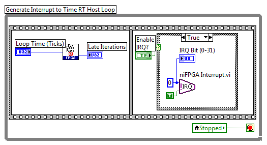
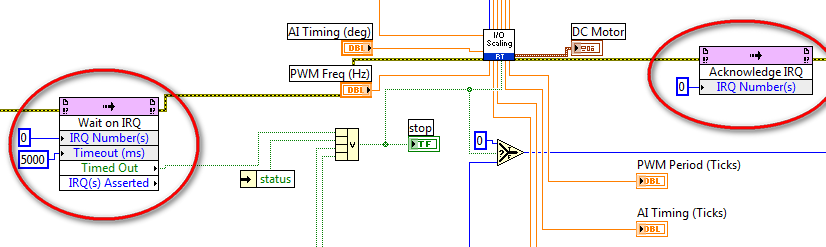
FPGA-IRQ in the custom VeriStand FPGA VI?
Hello
I built an FPGA VI custom to use in VeriStand. This FPGA VI contains the following IRQS:
Now I also have a VI in LabVIEW FPGA code that I want to use VeriStand. I changed it to use as a custom device, so I removed all of the FPGA code and replaced by indicators and controls so that I have can map device custom personalized in VeriStand FPGA.
But there is always the FPGA-IRQ, and I don't know what to do with these two nodes:
How can I use these knots in my VI of custom device or generally VeriStand?
Thanks for your help.
Kind regards
HScho
So finally I found a solution:
I disabled all the stuff IRQ. The main problem was that the model I wanted to use in VeriStand was inside a While loop. I had to remove the loop While VeriStand itself being the loop.
Kind regards
HScho


Maybe you are looking for
-
Where history complete on iso Safari?
On my desktop version of Safari, I can find almost anything in my browsing history. But on the iPhone (6 + iOS 9.3.2) available history is sparse and seemingly random. I cannot now find an important web page I've seen a few hours back. And back often
-
It is said there is something wrong with the network adapter driver and he gave me a Web site for the driver but it does not work He wants me to download what is called like this: install_vista_6213_1119.zip Additional information about the problem B
-
I think I removed internet explore 10 in accident I don't know how to do when I click on internet explore 10 that he takes on the desktop and I have a computer 2000 hp laptop
-
Can I develop pages OFA (extension EBS R12) without going through an instance of EBS in my computer?
Hello everyone,I am responsible for developing certain pages OFA in order to extend the EBS R12.The thing is, I don't have an instance of EBS in my computer. Can I simply create a connection to the Oracle database and work with it?Thank youKind regar
-
Hi, I have this problem: cooler of my probook 4525 s is very strong and working constantly.
It starts about 10 seconds after the ignition. Is - this normal - the Task Manager shows 0-10% CPU memory about 27%. The laptop is 3 months old, and he did not this loud before cooling. It started about a week there to see something being hotter (per