Alienware Aurora R3 CPU needs upgrade
I have the card with me now on the existing processor, but I heard somewhere that in order to replace the CPU, the computer must be shipped to the factory of Alienware. I have no experience in lieu of the CPU and do not wish to try myself. Someone at - it an order of magnitude estimate on how much it will cost me (parts included) if I send to Alienware?
Dell/Alienware don't post-purchase upgrades - you may be able to upgrade the processor slightly (Core i7 of second generation) but your upgrade options will be limited. If you don't want to do the work yourself, any store of the local computer can change the CPU - don't expect much in the way of speed. You'd be much better replace the hard drive with an SSD upgrade the processor, which is still in the League of the "Very fast" even today.
Tags: Dell Desktop
Similar Questions
-
Need help upgrading my alienware aurora
Here are all the technical features of cpu - z, keeping in mind both the original production (HD5670x2 crossfire) doesn't have a video card, I currently installed I picked up to 49.99 (half price) I was looking in the privateer, unit cooling, but even under the huge load, my computer runs at 27 c so... I have 12 GB memory, I want to game time to load faster... can I switch the processor without having to tear the entire computer? Maybe just the PSU and CPU? the cpu is removable for a best i7? that would help? cause I'm sure that the 12 GB of memory is not in desperate need of good memory? IM xcom2 to play and wait a good 2-3 minutes between the levels on the loading time... Anyway here is the screenshots, and below that is the cpu - z text file

TXT of CPU - Z report
-------------------------------------------------------------------------Binary files
-------------------------------------------------------------------------CPU - Z version 1.76.0.x64
Processors
-------------------------------------------------------------------------Number of processors 1
Number of threads 8APICs
-------------------------------------------------------------------------Processor 0
-Core 0
-Wire 0 0
-Thread 1 1
-Core 1
-0-2 wire
-Wire 1 3
-Core 2
-0-4 wire
-Wire 5 1
-Core 3
-0-6 wire
-Wire 1 7Timers
-------------------------------------------------------------------------Timer ACPI 3,580 MHz
Timer HPET 14,318 MHz
Timer perf 2,741 MHz
Sys 1,000 KHz timerInformation for processors
-------------------------------------------------------------------------Processor 1 ID = 0
Number of hearts 4 (max 8)
The number of threads 8 (max 16)
Name Intel Core i7 930
Codename Bloomfield
Specification Intel (r) Core i7 CPU 930 @ 2.80GHz
Package (platform ID) Socket 1366 LGA (0 x 1)
CPUID 6.A.5
CPUID extended 6. 1A
Core Stepping D0
The 45 nm technology
TDP limit 130.0 Watts
Basic speed 2940,5 MHz
Multiplier x Bus 22,0 x 133,7 MHz speed
2405,9 MHz rated Bus speed
Stock frequency of 2800 MHz
Instructions sets MMX, SSE, SSE2, SSE3, SSSE3, SSE4.1, SSE4.2, EM64T, VT - x
Data L1 cache 4 x 32 KB, size 8-way line set associative, 64 bytes
L1 instruction cache 4 x 32 KB, size 4-way set associative line, 64 bytes
L2 cache 4 x 256 KB, size 8-way line set associative, 64 bytes
Cache 8 MB L3, size 16-way set associative line, 64 bytes
FID/VID control YesTurbo Mode supported, enabled
3066 MHz Max turbo frequency
Max-non-Turbo report 21 x
Max turbo report 23 x
Max efficiency report 12 x
TDC limited 110 amps
Number of bus max 255
PCI peripheral device connected to the 255 bus, device 2, function 0
PCI peripheral device connected to the 255 bus, device 3, function 4Temperature 0 57 ° C (134 ° F) [0x2B] (Core #0)
Power supply 0 40.52 W (package)Thread dumps
-------------------------------------------------------------------------CPU thread 0
APIC ID 0
Topology Processor ID 0, Core ID 0, Thread ID 0
Type 01020001:
0000000Bh Max CPUID level
Level of position Max CPUID 80000008 h
Descriptor level 1, D, 32 KB, 2 wire (s) cache
Descriptor level 1, I, 32 k, 2 wire (s) cache
Descriptor cache level 2, U, 256 KB, 2 wire (s)
Descriptor cache level 3, U, 8 MB, 16 threadsCPUID
0 x 00000000 0x0000000B 0x756E6547 0x6C65746E 0x49656E69
0 x 00000001 0x000106A5 0 x 03100800 0x0098E3BD 0xBFEBFBFF
0 x 00000002 0x55035A01 0x00F0B2E4 0 x 00000000 0x09CA212C
0 x 00000003 0x00000000 0x00000000 0x00000000 0x00000000
0 x 00000004 0x0000003F 0x01C0003F 0x1C004121 0x00000000
0 x 00000004 0x1C004122 0x00C0003F 0x0000007F 0x00000000
0 x 00000004 0x1C004143 0x01C0003F 0x000001FF 0x00000000
0 x 00000004 0x1C03C163 0x03C0003F 0x00001FFF 0x00000002
0x00000005 00000040 0 x 0 x 00000040 0 x 00000003 0 x 00001120
0 x 00000006 0 x 00000003 0x00000002 0x00000001 0x00000000
0 x 00000007 0x00000000 0x00000000 0x00000000 0x00000000
0x00000008 0x00000000 0x00000000 0x00000000 0x00000000
0 x 00000009 0x00000000 0x00000000 0x00000000 0x00000000
0x0000000A 0 x 07300403 0 x 00000044 0x00000000 0 x 00000603
0x0000000B 0x00000001 0x00000002 0x00000100 0 x 00000003
0x0000000B 0 x 00000004 0x00000008 0 x 00000201 0 x 00000003
0x80000000 0 x 80000008 0x00000000 0x00000000 0x00000000
0 x 80000001 0x00000000 0x00000000 0x00000001 0 x 28100800
0 x 80000002 0x65746E49 0x2952286C 0x726F4320 0x4D542865
0 x 80000003 0 x 37692029 0 x 55504320 20202020 0 x 0 x 20202020
0 x 80000004 0 x 30333920 0 x 20402020 0x30382E32 0x007A4847
0 x 80000005 0x00000000 0x00000000 0x00000000 0x00000000
0 x 80000006 0x00000000 0x00000000 0 x 01006040 0x00000000
0 x 80000007 0x00000000 0x00000000 0x00000000 0x00000100
0 x 80000008 0 x 00003024 0x00000000 0x00000000 0x00000000MSR 0X0000001B, 0X00000000 0XFEE00900
MSR 0X0000003A 0X00000000 0X00000005
MSR 0X000001A0 0X00000000 0 X 00850089
MSR 0X000000CE 0X00000C00 0 X 00011501
MSR 0 X 00000017 0X00040000 0X00000000
MSR 0 X 00000035 0X00000000 0 X 00040008
MSR 0X000000C1 0X00000000 0X00000000
MSR 0X000000C2 0X00000000 0X00000000
MSR 0X000000C3 0X00000000 0X00000000
MSR 0X000000C4 0X00000000 0X00000000
MSR X 0 00000186 0X00000000 0X00000000
MSR X 0 00000187 0X00000000 0X00000000
MSR 0X000001AD 0X00000000 0 X 16161617
MSR 0X0000019A 0X00000000 0X00000000
MSR 0X000001A4 0X00000000 0X00000000
MSR 0X000001AC 0X00000000 0 X 03700410
MSR 0X000001FC 0X00000000 0X00000002
MSR 0 X 00000300 0X00000000 0XE0000001
MSR 0X0000019C 0X00000000 0X882B0000
MSR 0X000001A2 0X00000000 0 X 00641400
MSR 0XC0000103 0X00000000 0X00000000
MSR X 0 00000198 0X00000000 0 X 00000016
MSR X 0 00000199 0X00000000 0 X 00000016Chipset
-------------------------------------------------------------------------Northbridge Intel X 58 Rev.. 13
Southbridge Intel 82801IR (ICH10R) Rev. 00
Graphics interface PCI-Express
Width link PCI-E x 16
PCI-E Max Link width x 16
Type of DDR3 memory
Memory size 12 GB
Channel Triple
Frequency 668,3 MHz memory (02:10)
Latency CASE # (CL) 9.0
# For CASE # delay (tRCD) RAS 9
RAS # Precharge (tRP) 9
Cycle Time (tRAS) 24
Time to Row Refresh Cycle (tRFC) 74
Control rate (CR) 2 t
Uncore frequency 2673,2 MHz
Host Bridge 0 x 3405
Host Bridge 0x2C41
Host Bridge 0x2C01
Host Bridge 0x2C10
Host Bridge 0x2C11
Host Bridge 0x2C18
Host Bridge 0x2C19
Host Bridge 0x2C1C
Host Bridge 0x2C20
Host Bridge 0x2C21
Host Bridge 0x2C22
Host Bridge 0x2C23
Host Bridge 0x2C28
Host Bridge 0x2C29
Host Bridge 0x2C2A
Host Bridge 0x2C2B
Host Bridge 0x2C30
Host Bridge 0x2C31
Host Bridge 0x2C32
Host Bridge 0x2C33Memory SPD
-------------------------------------------------------------------------DIMM # 1
SMBus address 0 x 50
Type of DDR3 memory
UDIMM module format
Manufacturer (ID) Nanya Technology (7F7F7F0B000000000000)
Size 2048 MB
Bandwidth Max PC3-10700 (667 MHz)
NT2GC64B8HC0NF-CG part number
Serial number 085A 2264
Date week 51/year 10 manufacturing
Number of banks 8
Nominal voltage 1.50 Volts
EPP no
XMP no
AMP no
Timings JEDEC CL-tRCD-tRP-tRAS-tRC table @ frequency
JEDEC #1 6.0 - 6-6-17-23 @ 457 MHz
JEDEC #2 7.0 - 7-7-20-27 @ 533 MHz
JEDEC #3 8.0 - 8-8-22-30 MHz 609
JEDEC #4 9.0 - 9-9-24-33 @ 666 MHzDIMM # 2
SMBus address 0 x 51
Type of DDR3 memory
UDIMM module format
Manufacturer (ID) Nanya Technology (7F7F7F0B000000000000)
Size 2048 MB
Bandwidth Max PC3-10700 (667 MHz)
NT2GC64B8HC0NF-CG part number
Serial number D7592264
Date week 51/year 10 manufacturing
Number of banks 8
Nominal voltage 1.50 Volts
EPP no
XMP no
AMP no
Timings JEDEC CL-tRCD-tRP-tRAS-tRC table @ frequency
JEDEC #1 6.0 - 6-6-17-23 @ 457 MHz
JEDEC #2 7.0 - 7-7-20-27 @ 533 MHz
JEDEC #3 8.0 - 8-8-22-30 MHz 609
JEDEC #4 9.0 - 9-9-24-33 @ 666 MHzDIMM # 3
SMBus address 0 x 52
Type of DDR3 memory
UDIMM module format
Manufacturer (ID) Nanya Technology (7F7F7F0B000000000000)
Size 2048 MB
Bandwidth Max PC3-10700 (667 MHz)
NT2GC64B8HC0NF-CG part number
Serial number 085A 2262
Date week 51/year 10 manufacturing
Number of banks 8
Nominal voltage 1.50 Volts
EPP no
XMP no
AMP no
Timings JEDEC CL-tRCD-tRP-tRAS-tRC table @ frequency
JEDEC #1 6.0 - 6-6-17-23 @ 457 MHz
JEDEC #2 7.0 - 7-7-20-27 @ 533 MHz
JEDEC #3 8.0 - 8-8-22-30 MHz 609
JEDEC #4 9.0 - 9-9-24-33 @ 666 MHzDIMM # 4
SMBus address 0 x 53
Type of DDR3 memory
UDIMM module format
Manufacturer (ID) Nanya Technology (7F7F7F0B000000000000)
Size 2048 MB
Bandwidth Max PC3-10700 (667 MHz)
NT2GC64B8HC0NF-CG part number
Serial number 085A 2261
Date week 51/year 10 manufacturing
Number of banks 8
Nominal voltage 1.50 Volts
EPP no
XMP no
AMP no
Timings JEDEC CL-tRCD-tRP-tRAS-tRC table @ frequency
JEDEC #1 6.0 - 6-6-17-23 @ 457 MHz
JEDEC #2 7.0 - 7-7-20-27 @ 533 MHz
JEDEC #3 8.0 - 8-8-22-30 MHz 609
JEDEC #4 9.0 - 9-9-24-33 @ 666 MHzDIMM # 5
SMBus address 0 x 54
Type of DDR3 memory
UDIMM module format
Manufacturer (ID) Nanya Technology (7F7F7F0B000000000000)
Size 2048 MB
Bandwidth Max PC3-10700 (667 MHz)
NT2GC64B8HC0NF-CG part number
Serial number 36582262
Date week 51/year 10 manufacturing
Number of banks 8
Nominal voltage 1.50 Volts
EPP no
XMP no
AMP no
Timings JEDEC CL-tRCD-tRP-tRAS-tRC table @ frequency
JEDEC #1 6.0 - 6-6-17-23 @ 457 MHz
JEDEC #2 7.0 - 7-7-20-27 @ 533 MHz
JEDEC #3 8.0 - 8-8-22-30 MHz 609
JEDEC #4 9.0 - 9-9-24-33 @ 666 MHzDIMM # 6
SMBus address 0 x 55
Type of DDR3 memory
UDIMM module format
Manufacturer (ID) Nanya Technology (7F7F7F0B000000000000)
Size 2048 MB
Bandwidth Max PC3-10700 (667 MHz)
NT2GC64B8HC0NF-CG part number
Serial number 085A 2263
Date week 51/year 10 manufacturing
Number of banks 8
Nominal voltage 1.50 Volts
EPP no
XMP no
AMP no
Timings JEDEC CL-tRCD-tRP-tRAS-tRC table @ frequency
JEDEC #1 6.0 - 6-6-17-23 @ 457 MHz
JEDEC #2 7.0 - 7-7-20-27 @ 533 MHz
JEDEC #3 8.0 - 8-8-22-30 MHz 609
JEDEC #4 9.0 - 9-9-24-33 @ 666 MHzDIMM # 1
Registers SPD
00 01 02 03 04 05 06 07 08 09 0 HAS 0B 0E 0F 0D 0C
00 92 10 0 B 02 02 11 00 09 03 52 01 08 00 00 3 0C
10 69 78 69 30 69 11 20 89 70 03 3 3 00 F0 82 05
20 00 00 00 00 00 00 00 00 00 00 00 00 00 00 00 00
30 00 00 00 00 00 00 00 00 00 00 00 00 0F 11 01 01
40 00 00 00 00 00 00 00 00 00 00 00 00 00 00 00 00
50 00 00 00 00 00 00 00 00 00 00 00 00 00 00 00 00
60 00 00 00 00 00 00 00 00 00 00 00 00 00 00 00 00
70 00 00 00 00 00 83 0B 0D 10 51 08 5 A 22 64 AND 06 A1
4TH 4TH 80 54 32 47 43 36 34 42 38 48 43 30 46 2D 43
90 47 20 00 00 83 0 B 00 00 00 00 20 00 00 00 00 4
4 31 30 43 31 34 30 53 45 44 A0 4 54 30 35 31 36
B0 00 00 00 00 00 00 00 00 00 00 00 00 00 00 00 00
C0 00 00 00 00 00 00 00 00 00 00 00 00 00 00 00 00
D0 00 00 00 00 00 00 00 00 00 00 00 00 00 00 00 00
E0 00 00 00 00 00 00 00 00 00 00 00 00 00 00 00 00
F0 00 00 00 00 00 00 00 00 00 00 00 00 00 00 00 00DIMM # 2
Registers SPD
00 01 02 03 04 05 06 07 08 09 0 HAS 0B 0E 0F 0D 0C
00 92 10 0 B 02 02 11 00 09 03 52 01 08 00 00 3 0C
10 69 78 69 30 69 11 20 89 70 03 3 3 00 F0 82 05
20 00 00 00 00 00 00 00 00 00 00 00 00 00 00 00 00
30 00 00 00 00 00 00 00 00 00 00 00 00 0F 11 01 01
40 00 00 00 00 00 00 00 00 00 00 00 00 00 00 00 00
50 00 00 00 00 00 00 00 00 00 00 00 00 00 00 00 00
60 00 00 00 00 00 00 00 00 00 00 00 00 00 00 00 00
70 00 00 00 00 00 83 0B 0D 10 51 59 22 64 06 A1 D7
4TH 4TH 80 54 32 47 43 36 34 42 38 48 43 30 46 2D 43
90 47 20 00 00 83 0 B 00 00 00 00 20 00 00 00 00 4
4 31 30 43 31 34 30 53 45 44 A0 4 54 30 35 31 36
B0 00 00 00 00 00 00 00 00 00 00 00 00 00 00 00 00
C0 00 00 00 00 00 00 00 00 00 00 00 00 00 00 00 00
D0 00 00 00 00 00 00 00 00 00 00 00 00 00 00 00 00
E0 00 00 00 00 00 00 00 00 00 00 00 00 00 00 00 00
F0 00 00 00 00 00 00 00 00 00 00 00 00 00 00 00 00DIMM # 3
Registers SPD
00 01 02 03 04 05 06 07 08 09 0 HAS 0B 0E 0F 0D 0C
00 92 10 0 B 02 02 11 00 09 03 52 01 08 00 00 3 0C
10 69 78 69 30 69 11 20 89 70 03 3 3 00 F0 82 05
20 00 00 00 00 00 00 00 00 00 00 00 00 00 00 00 00
30 00 00 00 00 00 00 00 00 00 00 00 00 0F 11 01 01
40 00 00 00 00 00 00 00 00 00 00 00 00 00 00 00 00
50 00 00 00 00 00 00 00 00 00 00 00 00 00 00 00 00
60 00 00 00 00 00 00 00 00 00 00 00 00 00 00 00 00
70 00 00 00 00 00 83 0B 0D 10 51 08 5 A 22 62 AND 06 A1
4TH 4TH 80 54 32 47 43 36 34 42 38 48 43 30 46 2D 43
90 47 20 00 00 83 0 B 00 00 00 00 20 00 00 00 00 4
4 31 30 43 31 34 30 53 45 44 A0 4 54 30 35 31 36
B0 00 00 00 00 00 00 00 00 00 00 00 00 00 00 00 00
C0 00 00 00 00 00 00 00 00 00 00 00 00 00 00 00 00
D0 00 00 00 00 00 00 00 00 00 00 00 00 00 00 00 00
E0 00 00 00 00 00 00 00 00 00 00 00 00 00 00 00 00
F0 00 00 00 00 00 00 00 00 00 00 00 00 00 00 00 00DIMM # 4
Registers SPD
00 01 02 03 04 05 06 07 08 09 0 HAS 0B 0E 0F 0D 0C
00 92 10 0 B 02 02 11 00 09 03 52 01 08 00 00 3 0C
10 69 78 69 30 69 11 20 89 70 03 3 3 00 F0 82 05
20 00 00 00 00 00 00 00 00 00 00 00 00 00 00 00 00
30 00 00 00 00 00 00 00 00 00 00 00 00 0F 11 01 01
40 00 00 00 00 00 00 00 00 00 00 00 00 00 00 00 00
50 00 00 00 00 00 00 00 00 00 00 00 00 00 00 00 00
60 00 00 00 00 00 00 00 00 00 00 00 00 00 00 00 00
70 00 00 00 00 00 83 0B 0D 10 51 08 5 A 22 61 AND 06 A1
4TH 4TH 80 54 32 47 43 36 34 42 38 48 43 30 46 2D 43
90 47 20 00 00 83 0 B 00 00 00 00 20 00 00 00 00 4
4 31 30 43 31 34 30 53 45 44 A0 4 54 30 35 31 36
B0 00 00 00 00 00 00 00 00 00 00 00 00 00 00 00 00
C0 00 00 00 00 00 00 00 00 00 00 00 00 00 00 00 00
D0 00 00 00 00 00 00 00 00 00 00 00 00 00 00 00 00
E0 00 00 00 00 00 00 00 00 00 00 00 00 00 00 00 00
F0 00 00 00 00 00 00 00 00 00 00 00 00 00 00 00 00DIMM # 5
Registers SPD
00 01 02 03 04 05 06 07 08 09 0 HAS 0B 0E 0F 0D 0C
00 92 10 0 B 02 02 11 00 09 03 52 01 08 00 00 3 0C
10 69 78 69 30 69 11 20 89 70 03 3 3 00 F0 82 05
20 00 00 00 00 00 00 00 00 00 00 00 00 00 00 00 00
30 00 00 00 00 00 00 00 00 00 00 00 00 0F 11 01 01
40 00 00 00 00 00 00 00 00 00 00 00 00 00 00 00 00
50 00 00 00 00 00 00 00 00 00 00 00 00 00 00 00 00
60 00 00 00 00 00 00 00 00 00 00 00 00 00 00 00 00
70 00 00 00 00 00 83 0B 10 51 36 58 22 62 06 A1 0D
4TH 4TH 80 54 32 47 43 36 34 42 38 48 43 30 46 2D 43
90 47 20 00 00 83 0 B 00 00 00 00 20 00 00 00 00 4
4 31 30 43 31 34 30 53 45 44 A0 4 54 30 35 31 36
B0 00 00 00 00 00 00 00 00 00 00 00 00 00 00 00 00
C0 00 00 00 00 00 00 00 00 00 00 00 00 00 00 00 00
D0 00 00 00 00 00 00 00 00 00 00 00 00 00 00 00 00
E0 00 00 00 00 00 00 00 00 00 00 00 00 00 00 00 00
F0 00 00 00 00 00 00 00 00 00 00 00 00 00 00 00 00DIMM # 6
Registers SPD
00 01 02 03 04 05 06 07 08 09 0 HAS 0B 0E 0F 0D 0C
00 92 10 0 B 02 02 11 00 09 03 52 01 08 00 00 3 0C
10 69 78 69 30 69 11 20 89 70 03 3 3 00 F0 82 05
20 00 00 00 00 00 00 00 00 00 00 00 00 00 00 00 00
30 00 00 00 00 00 00 00 00 00 00 00 00 0F 11 01 01
40 00 00 00 00 00 00 00 00 00 00 00 00 00 00 00 00
50 00 00 00 00 00 00 00 00 00 00 00 00 00 00 00 00
60 00 00 00 00 00 00 00 00 00 00 00 00 00 00 00 00
70 00 00 00 00 00 83 0B 0D 10 51 08 5 A 22 63 AND 06 A1
4TH 4TH 80 54 32 47 43 36 34 42 38 48 43 30 46 2D 43
90 47 20 00 00 83 0 B 00 00 00 00 20 00 00 00 00 4
4 31 30 43 31 34 30 53 45 44 A0 4 54 30 35 31 36
B0 00 00 00 00 00 00 00 00 00 00 00 00 00 00 00 00
C0 00 00 00 00 00 00 00 00 00 00 00 00 00 00 00 00
D0 00 00 00 00 00 00 00 00 00 00 00 00 00 00 00 00
E0 00 00 00 00 00 00 00 00 00 00 00 00 00 00 00 00
F0 00 00 00 00 00 00 00 00 00 00 00 00 00 00 00 00Monitoring
-------------------------------------------------------------------------Model of motherboard 04VWF2 (0 x 00000189 - 0x004D8240)
LPCIO
-------------------------------------------------------------------------LPCIO seller are
LPCIO model F71882F
LPCIO Vendor ID 0 x 1934
LPCIO Chip ID 0 x 541
0x4E config Mode i/o address
Configuration Mode NDA 0x4
Saves the configuration mode
00 01 02 03 04 05 06 07 08 09 0 HAS 0B 0E 0F 0D 0C
00 FF FF 00 FF FF FF FF FF 04 FF FF FF FF FF FF FF
10 FF FF FF FF FF FF FF FF FF FF FF FF FF FF FF FF
20 05 41 20 19 34 00 00 30 44 00 40 60 08 00 00 0F
30 01 FF FF FF FF FF FF FF FF FF FF FF FF FF FF FF
40 FF FF FF FF FF FF FF FF FF FF FF FF FF FF FF FF
50 FF FF FF FF FF FF FF FF FF FF FF FF FF FF FF FF
60 0 A 00 FF FF FF FF FF FF FF FF FF FF FF FF FF FF
70 00 FF FF FF FF FF FF FF FF FF FF FF FF FF FF FF
Register space LPC, base address = 0x0A00Hardware monitors
-------------------------------------------------------------------------Door F71882F hardware monitor
Voltage Volt 3.39 0 [0xD4] (+ 3, 3V)
Voltage Volt 1 1.24 [0x9B] (CPU VCORE)
Voltage Volt 2 2.05 [0x80] (VIN2)
Voltage Volt 3 1.21 [0 x 67] (VIN3)
Voltage Volt 4 5.05 0 x [78] (+ 5V)
Voltage Volt 5 12.14 [0x8A] (+ 12V)
Voltage 6 1.78 Volts [0x6F] (VIN6)
Voltage Volt 7 3.38 [0xD3] (VSB3V)
Voltage Volt 8 3.23 [0xCA] (VBAT)
Temperature 0 to 40 ° C (104 ° F) 0 x [28] (TMPIN0)
Temperature 1 59 ° C (138 ° F) [0x3B] (TMPIN1)
2 temperature of 53 ° C (127 ° F) 0 x [35] (TMPIN2)
Fan 0 1205 RPM [0x4DD] (FANIN0)
Fan PWM 0 100 pc [0xFF] (CPU)
Fan PWM 1 100 pc [0xFF] (System 1 fan)
Fan PWM 2 100 pc [0xFF] (System Fan 2)
Fan PWM 3 100 pc [0xFF] (3 system fan)
Register space LPC, base address = 0x0A0000 01 02 03 04 05 06 07 08 09 0 HAS 0B 0E 0F 0D 0C
FF 00 03 00 00 FF FF FF FF FF FF 01 00 55 4 00 00
10 00 00 00 00 FF FF FF FF FF FF FF FF FF FF FF FF
20 D4 5F 75 49 78 8 B 6F D3 CA FF FF FF FF FF FF FF
30 FF FF FF FF FF FF FF FF FF FF FF FF FF FF FF FF
40 FF FF FF FF FF FF FF FF FF FF FF FF FF FF FF FF
50 FF FF FF FF FF FF FF FF FF FF 03 04 10 19 34 FF
60 00 00 00 00 FF FF 00 00 00 00 FF 08 40 24 00 FF
70 FF FF FF 28 3 B FF 35 FF FF FF FF FF FF FF FF FF
80 FF FF FF FF FF FF FF FF FF FF FF FF FF FF A8 FF
90 00 0E 0E 00 16 00 FF FF 00 FF 24 01 02 55 FF 1 A
A0 DF 04 E0 01 4 48 3 A 34 00 09 17 28 58 1 2D 04D
B0 FF 05 03 FF 3 32 28 C 5 C 0F 1E 0 B 00 12 2 HAS IN THE 30 0E
C0 FF 05 03 FF 3 32 28 C 5 C 0F 1E 0 B 00 12 2 HAS IN THE 30 0F
D0 0F FF 05 03 FF 3 32 28 C 5 C 1 0 B 00 12 2 HAS IN THE 30 0F
E0 FF FF FF FF FF FF FF FF FF FF FF FF FF FF FF FF
F0 00 00 00 00 00 00 3 B FF 03 43 00 FF FF FF FF FFMonitor hardware NVIDIA NVAPI
Voltage Volt 0 0.98 [0x3CF] (VIN0)
Temperature 0 34 ° C (93 ° F) 0 x [22] (TMPIN0)
0 21 0 x [15] pc PWM fan (FANPWMIN0)
Clock speed 324.00 0 MHz [0 x 144] (chart)
Clock speed 1 324.00 MHz [0 x 144] (memory)PCI devices
-------------------------------------------------------------------------Register PCI Express, base address space = 0x0E0000000
Description Host Bridge
Bus location 0 (0x00), device 0 (0x00), function 0 (0x00)
Common collector
Vendor ID 0 x 8086
ID of the template 0 x 3405
Revision ID 0x13
PI 0X00
Subclass 0 x 00
BaseClass 0x06
Cache line 0x00
Latency 0 x 00
Header 0x00
PCI header
Subprovider ID 0 x 1028
ID subsystem 0x02F7
. Int. line 0x00
Int. PIN 0 x 00
Capacity PCI
Caps of the class reported Message interrupts
Caps offset 0 x 60
Capacity PCI
Caps of class PCI Express
Caps offset 0 x 90
Device type root Port of PCI - E root complex
Port 0
Version 2.0
Built-in physical location
Link width 4 x (max. 4 x)
Capacity PCI
Caps of class power management
Caps offset 0xE0
Version 1.2 of the CAPS
Extended features
Advanced Error Reporting class caps
Caps offset 0 x 100
Caps 0xD class
Caps offset 0 x 150
Caps of the vendor specific class
Caps offset 0 x 160
Vendor ID 2
Size 12
PCI registers
00 01 02 03 04 05 06 07 08 09 0 HAS 0B 0E 0F 0D 0C
00 86 80 05 34 00 00 10 00 13 00 00 06 00 00 00 00
10 00 00 00 00 00 00 00 00 00 00 00 00 00 00 00 00
20 00 00 00 00 00 00 00 00 00 00 00 00 28 10 F7 02
30 00 00 00 00 60 00 00 00 00 00 00 00 00 00 00 00
40 00 00 00 00 00 00 00 00 00 00 00 00 00 00 00 00
50 00 00 D1 FE 00 00 00 00 00 00 00 00 00 00 00 00
60 05 90 02 01 00 00 00 00 00 00 00 00 00 00 00 00
70 00 00 00 00 00 00 00 00 00 00 00 00 00 00 00 00
80 00 00 00 00 00 00 00 00 00 00 00 00 00 00 00 00
90 10 E0 42 00 20 80 00 00 00 00 00 00 41 3 3 B 00
A0 00 00 41 30 00 00 00 00 07 00 01 00 00 00 00 C0
B0 00 00 00 00 00 00 00 09 00 00 00 00 00 00 00 3F
C0 01 00 00 00 00 00 00 00 00 00 00 00 00 00 00 00
D0 00 00 00 00 00 00 00 00 00 00 00 00 00 00 00 00
E0 01 00 03 C8 08 00 00 00 00 00 00 00 00 00 00 00
F0 00 00 00 00 00 00 00 00 00 00 00 00 00 00 00 00
100 01 00 01 15 00 00 00 00 00 00 00 00 30 20 06 00
110 00 00 00 00 00 20 00 00 00 00 00 00 00 00 00 00
120 00 00 00 00 00 00 00 00 00 00 00 00 00 00 00 00
130 00 00 00 00 00 00 00 00 00 00 00 00 00 00 00 00Description PCI to PCI Bridge
Bus location 0 (0x00), device 1 (0x01), function 0 (0x00)
Common collector
Vendor ID 0 x 8086
ID of the template 0 x 3408
Revision ID 0x13
PI 0X00
Subclass 0 x 04
BaseClass 0x06
Line cache 0x40
Latency 0 x 00
Header 0x01
PCI header
Main bus 0 x 00
Secondary bus 0 x 09
. Int. line 0x00
Int. PIN 0 x 00
Capacity PCI
Caps class subsystem of the seller
Caps offset 0 x 40
Subprovider ID 0 x 1028
ID subsystem 0x02F7
Capacity PCI
Caps of the class reported Message interrupts
Caps offset 0 x 60
Capacity PCI
Caps of class PCI Express
Caps offset 0 x 90
Device type root Port of PCI - E root complex
Port 0
Version 2.0
Physical location #0
Detection of presence no.
Link 0 width x (max 4 x)
Capacity PCI
Caps of class power management
Caps offset 0xE0
Version 1.2 of the CAPS
Extended features
Advanced Error Reporting class caps
Caps offset 0 x 100
Caps 0xD class
Caps offset 0 x 150
Caps of the vendor specific class
Caps offset 0 x 160
Vendor ID 2
Size 12
PCI registers
00 01 02 03 04 05 06 07 08 09 0 HAS 0B 0E 0F 0D 0C
00 86 80 08 34 04 05 10 00 13 00 04 06 40 00 01 00
10 00 00 00 00 00 00 00 00 00 09 09 00 00 00 00 F0
20 F0 FF 00 00 F1 FF 01 00 00 00 00 00 00 00 00 00
30 00 00 00 00 40 00 00 00 00 00 00 00 00 00 02 00
40 0D 60 00 00 28 10 02 00 00 00 00 00 00 00 00 F7
50 00 00 00 00 00 00 00 00 00 00 00 00 00 00 00 00
60 05 90 02 01 00 00 00 00 00 00 00 00 00 00 00 00
70 00 00 00 00 00 00 00 00 00 00 00 00 00 00 00 00
80 00 00 00 00 00 00 00 00 00 00 00 00 00 00 00 00
90 10 E0 42 01 21 80 00 00 00 00 00 00 42 3 3 B 00
A0 00 00 01 10 00 00 00 00 03 08 00 00 00 01 00 C0
B0 00 00 00 00 00 00 00 09 00 00 00 00 00 00 00 3F
C0 02 00 00 00 00 00 00 00 00 00 00 00 00 00 00 00
D0 00 00 00 00 00 00 00 00 00 00 00 00 00 00 00 00
E0 01 00 03 C8 08 00 00 00 00 00 00 00 00 00 00 00
F0 00 00 00 00 00 00 00 00 00 00 00 00 00 00 00 00
100 01 00 01 15 00 00 00 00 00 00 00 00 30 20 06 00
110 00 00 00 00 00 20 00 00 00 00 00 00 00 00 00 00
120 00 00 00 00 00 00 00 00 00 00 00 00 00 00 00 00
130 00 00 00 00 00 00 00 00 00 00 00 00 00 00 00 00Description PCI to PCI Bridge
Bus location 0 (0x00), device 3 (0x03), function 0 (0x00)
Common collector
Vendor ID 0 x 8086
The model 0x340A ID
Revision ID 0x13
PI 0X00
Subclass 0 x 04
BaseClass 0x06
Line cache 0x40
Latency 0 x 00
Header 0x01
PCI header
Main bus 0 x 00
Secondary bus 0 x 08
. Int. line 0x00
Int. PIN 0 x 00
Capacity PCI
Caps class subsystem of the seller
Caps offset 0 x 40
Subprovider ID 0 x 1028
ID subsystem 0x02F7
Capacity PCI
Caps of the class reported Message interrupts
Caps offset 0 x 60
Capacity PCI
Caps of class PCI Express
Caps offset 0 x 90
Device type root Port of PCI - E root complex
Port 0
Version 2.0
Physical location #0
Presence detection Yes
Link width 16 x (16 x max.)
Capacity PCI
Caps of class power management
Caps offset 0xE0
Version 1.2 of the CAPS
Extended features
Advanced Error Reporting class caps
Caps offset 0 x 100
Caps 0xD class
Caps offset 0 x 150
Caps of the vendor specific class
Caps offset 0 x 160
Vendor ID 2
Size 12
PCI registers
00 01 02 03 04 05 06 07 08 09 0 HAS 0B 0E 0F 0D 0C
00 86 80 0 A 34 07 05 10 00 13 00 04 06 40 00 01 00
10 00 00 00 00 00 00 00 00 00 08 08 00 00 20 E0 E0
20 00 F0 FA FB 01 THIS F1 DF 00 00 00 00 00 00 00 00
30 00 00 00 00 40 00 00 00 00 00 00 00 00 00 1 A 00
40 0D 60 00 00 28 10 02 00 00 00 00 00 00 00 00 F7
50 00 00 00 00 00 00 00 00 00 00 00 00 00 00 00 00
60 05 90 02 01 00 00 00 00 00 00 00 00 00 00 00 00
70 00 00 00 00 00 00 00 00 00 00 00 00 00 00 00 00
80 00 00 00 00 00 00 00 00 00 00 00 00 00 00 00 00
90 10 E0 00 3D 42 01 21 80 00 00 00 00 00 00 02 3-B
A0 00 00 01 71 00 00 00 00 C0 03 48 01 00 00 01 00
B0 00 00 00 00 00 00 00 09 00 00 00 00 00 00 00 3F
C0 02 00 00 00 00 00 00 00 00 00 00 00 00 00 00 00
D0 00 00 00 00 00 00 00 00 00 00 00 00 00 00 00 00
E0 01 00 03 C8 08 00 00 00 00 00 00 00 00 00 00 00
F0 00 00 00 00 00 00 00 00 00 00 00 00 00 00 00 00
100 01 00 01 15 00 00 00 00 00 00 00 00 30 20 06 00
110 00 00 00 00 00 20 00 00 00 00 00 00 00 00 00 00
120 00 00 00 00 00 00 00 00 00 00 00 00 00 00 00 00
130 00 00 00 00 00 00 00 00 00 00 00 00 00 00 00 00Description PCI to PCI Bridge
Bus location 0 (0x00), device 7 (0x07), function 0 (0x00)
Common collector
Vendor ID 0 x 8086
The model 0x340E ID
Revision ID 0x13
PI 0X00
Subclass 0 x 04
BaseClass 0x06
Line cache 0x40
Latency 0 x 00
Header 0x01
PCI header
Main bus 0 x 00
Secondary bus 0 x 07
. Int. line 0x00
Int. PIN 0 x 00
Capacity PCI
Caps class subsystem of the seller
Caps offset 0 x 40
Subprovider ID 0 x 1028
ID subsystem 0x02F7
Capacity PCI
Caps of the class reported Message interrupts
Caps offset 0 x 60
Capacity PCI
Caps of class PCI Express
Caps offset 0 x 90
Device type root Port of PCI - E root complex
Port 0
Version 2.0
Physical location #0
Detection of presence no.
Link 0 width x (8 x max)
Capacity PCI
Caps of class power management
Caps offset 0xE0
Version 1.2 of the CAPS
Extended features
Advanced Error Reporting class caps
Caps offset 0 x 100
Caps 0xD class
Caps offset 0 x 150
Caps of the vendor specific class
Caps offset 0 x 160
Vendor ID 2
Size 12
PCI registers
00 01 02 03 04 05 06 07 08 09 0 HAS 0B 0E 0F 0D 0C
00 86 80 0E 34 04 05 10 00 13 00 04 06 40 00 01 00
10 00 00 00 00 00 00 00 00 00 07 07 00 00 00 00 F0
20 F0 FF 00 00 F1 FF 01 00 00 00 00 00 00 00 00 00
30 00 00 00 00 40 00 00 00 00 00 00 00 00 00 02 00
40 0D 60 00 00 28 10 02 00 00 00 00 00 00 00 00 F7
50 00 00 00 00 00 00 00 00 00 00 00 00 00 00 00 00
60 05 90 02 01 00 00 00 00 00 00 00 00 00 00 00 00
70 00 00 00 00 00 00 00 00 00 00 00 00 00 00 00 00
80 00 00 00 00 00 00 00 00 00 00 00 00 00 00 00 00
90 10 E0 42 01 21 80 00 00 00 00 00 00 82 3 3 B 00
A0 00 00 01 10 00 00 00 00 03 08 00 00 00 01 00 C0
B0 00 00 00 00 00 00 00 09 00 00 00 00 00 00 00 3F
C0 02 00 00 00 00 00 00 00 00 00 00 00 00 00 00 00
D0 00 00 00 00 00 00 00 00 00 00 00 00 00 00 00 00
E0 01 00 03 C8 08 00 00 00 00 00 00 00 00 00 00 00
F0 00 00 00 00 00 00 00 00 00 00 00 00 00 00 00 00
100 01 00 01 15 00 00 00 00 00 00 00 00 30 20 06 00
110 00 00 00 00 00 20 00 00 00 00 00 00 00 00 00 00
120 00 00 00 00 00 00 00 00 00 00 00 00 00 00 00 00
130 00 00 00 00 00 00 00 00 00 00 00 00 00 00 00 00Description PCI to PCI Bridge
Bus location 0 (0x00), device 9 (0 x 09), function 0 (0x00)
Common collector
Vendor ID 0 x 8086
ID of the template 0 x 3410
Revision ID 0x13
PI 0X00
Subclass 0 x 04
BaseClass 0x06
Line cache 0x40
Latency 0 x 00
Header 0x01
PCI header
Main bus 0 x 00
Secondary bus 0 x 06
. Int. line 0x00
Int. PIN 0 x 00
Capacity PCI
Caps class subsystem of the seller
Caps offset 0 x 40
Subprovider ID 0 x 1028
ID subsystem 0x02F7
Capacity PCI
Caps of the class reported Message interrupts
Caps offset 0 x 60
Capacity PCI
Caps of class PCI Express
Caps offset 0 x 90
Device type root Port of PCI - E root complex
Port 0
Version 2.0
Physical location #0
Detection of presence no.
Link 0 width x (8 x max)
Capacity PCI
Caps of class power management
Caps offset 0xE0
Version 1.2 of the CAPS
Extended features
Advanced Error Reporting class caps
Caps offset 0 x 100
Caps 0xD class
Caps offset 0 x 150
PCI registers
00 01 02 03 04 05 06 07 08 09 0 HAS 0B 0E 0F 0D 0C
00 86 80 10 34 04 05 10 00 13 00 04 06 40 00 01 00
10 00 00 00 00 00 00 00 00 00 06 06 00 00 00 00 F0
20 F0 FF 00 00 F1 FF 01 00 00 00 00 00 00 00 00 00
30 00 00 00 00 40 00 00 00 00 00 00 00 00 00 02 00
40 0D 60 00 00 28 10 02 00 00 00 00 00 00 00 00 F7
50 00 00 00 00 00 00 00 00 00 00 00 00 00 00 00 00
60 05 90 02 01 00 00 00 00 00 00 00 00 00 00 00 00
70 00 00 00 00 00 00 00 00 00 00 00 00 00 00 00 00
80 00 00 00 00 00 00 00 00 00 00 00 00 00 00 00 00
90 10 E0 42 01 21 80 00 00 00 00 00 00 82 3 3 B 00
A0 00 00 01 10 00 00 00 00 03 08 00 00 00 01 00 C0
B0 00 00 00 00 00 00 00 09 00 00 00 00 00 00 00 3F
C0 02 00 00 00 00 00 00 00 00 00 00 00 00 00 00 00
D0 00 00 00 00 00 00 00 00 00 00 00 00 00 00 00 00
E0 01 00 03 C8 08 00 00 00 00 00 00 00 00 00 00 00
F0 00 00 00 00 00 00 00 00 00 00 00 00 00 00 00 00
100 01 00 01 15 00 00 00 00 00 00 00 00 30 20 06 00
110 00 00 00 00 00 20 00 00 00 00 00 00 00 00 00 00
120 00 00 00 00 00 00 00 00 00 00 00 00 00 00 00 00
130 00 00 00 00 00 00 00 00 00 00 00 00 00 00 00 00Peripheral system description
Bus location 0 (0x00), device 20 (0x14), function 0 (0x00)
Common collector
Vendor ID 0 x 8086
The model 0x342E ID
Revision ID 0x13
PI 0X00
Subclass 0 x 00
BaseClass 0x08
Line cache 0x40
Latency 0 x 00
Header 0x80
PCI header
Subprovider ID 0x0000
Subsystem ID 0x0000
. Int. line 0x00
Int. PIN 0 x 00
Capacity PCI
Caps of class PCI Express
Caps offset 0 x 40
Built-in device peripheral complex root of endpoint type
Port 0
Version 2.0
Link 0 width x (max 0 x)
PCI registers
00 01 02 03 04 05 06 07 08 09 0 HAS 0B 0E 0F 0D 0C
00 86 80 2ND 34 00 00 10 00 13 00 00 08 40 00 80 00
10 00 00 00 00 00 00 00 00 00 00 00 00 00 00 00 00
20 00 00 00 00 00 00 00 00 00 00 00 00 00 00 00 00
30 00 00 00 00 40 00 00 00 00 00 00 00 00 00 00 00
40 10 00 92 00 00 80 00 00 00 00 00 00 00 3B 00 F4
50 00 00 00 10 00 00 00 00 07 00 00 00 00 01 00 C0
60 00 00 00 00 00 80 00 00 00 00 00 00 00 3B 00 F4
70 00 00 00 10 00 00 00 00 07 00 00 00 00 00 00 C0
80 00 00 00 00 00 00 00 00 00 00 FF FF FF FF 07 00
90 00 00 00 00 00 00 00 00 48 10 05 00 14 03 00 EC
A0 00 00 00 00 00 00 00 00 09 00 80 00 00 00 00 BF
B0 00 00 FF FF FF FF 07 00 00 00 00 00 00 00 00 00
C0 00 00 FF FF FF FF 07 00 00 00 00 00 00 00 00 00
D0 00 00 00 BC 00 00 00 3 03 00 00 00 00 00 00 FC
E0 FF FF FF FF 00 00 00 00 00 00 00 00 00 00 00 00
F0 ED 74 FF 3F 00 00 00 00 00 00 00 00 00 00 7F C4
100 00 00 00 00 00 00 00 00 00 00 01 00 E0 THIS FB 00
110 FB FC 00 00 00 00 00 00 00 00 00 00 00 00 00 00
120 00 00 00 00 E0 THIS FB FC 00 00 00 00 00 00 00 00
130 00 00 00 00 00 00 00 00 00 00 00 00 00 00 00 FBPeripheral system description
Bus location 0 (0x00), device 20 (0x14), function 1 (0x01)
Common collector
Vendor ID 0 x 8086
ID of the template 0 x 3422
Revision ID 0x13
PI 0X00
Subclass 0 x 00
BaseClass 0x08
Line cache 0x40
Latency 0 x 00
Header 0x80
PCI header
Subprovider ID 0x0000
Subsystem ID 0x0000
. Int. line 0x00
Int. PIN 0 x 00
Capacity PCI
Caps of class PCI Express
Caps offset 0 x 40
Built-in device peripheral complex root of endpoint type
Port 0
Version 2.0
Link 0 width x (max 0 x)
PCI registers
00 01 02 03 04 05 06 07 08 09 0 HAS 0B 0E 0F 0D 0C
00 86 80 22 34 00 00 10 00 13 00 00 08 40 00 80 00
10 00 00 00 00 00 00 00 00 00 00 00 00 00 00 00 00
20 00 00 00 00 00 00 00 00 00 00 00 00 00 00 00 00
30 00 00 00 00 40 00 00 00 00 00 00 00 00 00 00 00
40 10 00 92 00 00 80 00 00 00 00 00 00 00 3B 00 F4
50 00 00 00 10 00 00 00 00 07 00 00 00 00 01 00 C0
60 00 00 00 00 00 80 00 00 00 00 00 00 00 3B 00 F4
70 00 00 00 10 00 00 00 00 07 00 00 00 15 00 00 C0
80 00 00 00 00 00 00 00 00 00 00 00 00 00 00 00 00
90 00 00 00 00 00 00 00 00 00 00 00 00 00 00 00 BF
A0 00 00 00 00 00 03 00 02 00 00 83 01 00 00 00 00
B0 A5 06 01 00 00 00 00 00 00 00 00 00 00 00 00 00
C0 00 00 00 00 00 00 00 00 00 00 00 00 14 00 00 C7
D0 04 04 04 00 04 04 04 00 00 00 00 00 00 15 00 00
E0 00 00 00 00 00 00 00 00 00 00 00 00 00 00 00 00
F0 00 00 00 00 00 00 00 00 00 00 00 00 00 00 00 BF
100 00 00 00 00 00 00 00 00 00 03 00 02 00 00 83 01
110 00 00 00 00 06 01 00 00 00 00 00 00 00 00 00 A5
120 00 00 00 00 00 00 00 00 00 00 00 00 00 00 00 00
C7 130 14 00 00 04 04 04 00 04 04 04 00 00 00 00 00Peripheral system description
Bus location 0 (0x00), device 20 (0x14), function 2 (0x02)
Common collector
Vendor ID 0 x 8086
ID of the template 0 x 3423
Revision ID 0x13
PI 0X00
Subclass 0 x 00
BaseClass 0x08
Line cache 0x40
Latency 0 x 00
Header 0x80
PCI header
Subprovider ID 0x0000
Subsystem ID 0x0000
. Int. line 0x00
Int. PIN 0 x 00
Capacity PCI
Caps of class PCI Express
Caps offset 0 x 40
Built-in device peripheral complex root of endpoint type
Port 0
Version 2.0
Link 0 width x (max 0 x)
PCI registers
00 01 02 03 04 05 06 07 08 09 0 HAS 0B 0E 0F 0D 0C
00 86 80 23 34 00 00 10 00 13 00 00 08 40 00 80 00
10 00 00 00 00 00 00 00 00 00 00 00 00 00 00 00 00
20 00 00 00 00 00 00 00 00 00 00 00 00 00 00 00 00
30 00 00 00 00 40 00 00 00 00 00 00 00 00 00 00 00
40 10 00 92 00 00 80 00 00 00 00 00 00 00 3B 00 F4
50 00 00 00 10 00 00 00 00 07 00 00 00 00 01 00 C0
60 00 00 00 00 00 80 00 00 00 00 00 00 00 3B 00 F4
70 00 00 00 10 00 00 00 00 07 00 00 00 00 00 00 C0
A4 80 80 A0 01 50 02 AA AA 00 00 00 65 15 00 00 A8
90 00 00 00 00 24 00 00 00 04 08 00 00 22 05 00 00
A0 00 00 00 00 00 00 00 00 00 00 00 00 00 00 00 00
B0 00 00 00 00 00 00 00 00 00 00 00 00 00 00 00 00
C0 01 00 00 00 00 00 00 00 00 00 00 00 00 42 00 00
D0 00 00 00 00 00 08 08 92 9 BB 00 35 00 00 10 00 D
E0 40 58 05 00 FB 03 00 00 FF 07 00 00 00 00 00 00
F0 00 00 00 00 00 00 00 00 00 00 00 00 00 00 00 00
100 00 00 00 00 00 00 00 00 00 00 00 00 00 00 00 00
110 00 00 00 00 00 00 00 00 00 00 00 00 00 00 00 00
120 00 00 00 00 00 00 00 00 00 00 00 00 00 00 00 00
130 00 00 00 00 00 00 00 00 00 00 00 00 00 00 00 00Peripheral system description
Bus location 0 (0x00), device 20 (0x14), function 3 (0x03)
Common collector
Vendor ID 0 x 8086
ID of the template 0 x 3438
Revision ID 0x13
PI 0X00
Subclass 0 x 00
BaseClass 0x08
Line cache 0x40
Latency 0 x 00
Header 0x80
PCI header
Subprovider ID 0x0000
Subsystem ID 0x0000
. Int. line 0x00
Int. PIN 0 x 00
PCI registers
00 01 02 03 04 05 06 07 08 09 0 HAS 0B 0E 0F 0D 0C
00 86 80 38 34 00 00 00 00 13 00 00 08 40 00 80 00
10 00 00 00 00 00 00 00 00 00 00 00 00 00 00 00 00
20 00 00 00 00 00 00 00 00 00 00 00 00 00 00 00 00
30 00 00 00 00 00 00 00 00 00 00 00 00 00 00 00 00
40 00 00 00 00 00 00 00 00 00 00 00 00 00 00 00 00
50 00 00 00 00 00 00 00 00 00 00 00 00 00 00 00 00
60 00 00 00 00 00 00 00 00 00 00 00 00 00 00 00 00
70 00 00 00 00 00 00 00 00 00 00 00 00 00 00 00 00
80 00 00 00 00 0 B 00 00 00 00 00 00 00 00 00 00 00
90 00 00 00 00 0 B 00 00 00 00 00 00 00 00 00 00 00
A0 00 00 00 00 0 B 00 00 00 00 00 00 00 00 00 00 00
B0 00 00 00 00 00 00 00 00 00 00 00 00 00 00 00 00
C0 00 00 00 00 00 00 00 00 00 00 00 00 00 00 00 00
D0 00 00 00 00 00 00 00 00 00 00 00 00 00 00 00 00
E0 00 00 DC 00 00 00 00 00 00 00 00 00 00 C8 B4 A8
F0 00 00 00 7F 00 00 00 00 40 07 00 00 00 00 D3 0DDescription USB UHCI controller)
Bus location 0 (0x00), 26 (0x1A) device, function 0 (0x00)
Common collector
Vendor ID 0 x 8086
The model 0x3A37 ID
Revision ID 0x00
PI 0X00
Subclass 0 x 03
BaseClass 0x0C
Cache line 0x00
Latency 0 x 00
Header 0x80
PCI header
Address 4 (port) 0x0000A400
Subprovider ID 0 x 1028
ID subsystem 0x02F7
Int line. 0x10
Int. PIN 0 x 01
Capacity PCI
Class caps 0 x 13
Caps offset 0 x 50
PCI registers
00 01 02 03 04 05 06 07 08 09 0 HAS 0B 0E 0F 0D 0C
00 86 80 37 3 A 05 00 90 02 00 00 03 00 00 80 00 0C
10 00 00 00 00 00 00 00 00 00 00 00 00 00 00 00 00
20 01 A4 00 00 00 00 00 00 00 00 00 00 28 10 F7 02
30 00 00 00 00 50 00 00 00 00 00 00 00 10 01 00 00
40 00 00 00 00 00 00 00 00 00 00 00 00 00 00 00 00
50 13 06 03 00 00 00 00 00 00 00 00 00 00 00 00 00
60 10 00 00 00 00 00 00 00 00 00 00 00 00 00 00 00
70 00 00 00 00 00 00 00 00 00 00 00 00 00 00 00 00
80 00 00 00 00 00 00 00 00 00 00 00 00 00 00 00 00
90 00 00 00 00 00 00 00 00 00 00 00 00 00 00 00 00
A0 00 00 00 00 00 00 00 00 00 00 00 00 00 00 00 00
B0 00 00 00 00 00 00 00 00 00 00 00 00 00 00 00 00
C0 00 20 00 00 00 00 00 00 00 00 01 00 00 00 00 00
D0 00 00 00 00 00 00 00 00 00 00 00 00 00 00 00 00
E0 00 00 00 00 00 00 00 00 00 00 00 00 00 00 00 00
F0 00 00 00 00 00 00 00 00 86 04 00 00 00 00 00 0FDescription USB UHCI controller)
Bus location 0 (0x00), 26 (0x1A) device, function 1 (0x01)
Common collector
Vendor ID 0 x 8086
The model 0x3A38 ID
Revision ID 0x00
PI 0X00
Subclass 0 x 03
BaseClass 0x0C
Cache line 0x00
Latency 0 x 00
Header 0x00
PCI header
Address 4 (port) 0x0000A480
Subprovider ID 0 x 1028
ID subsystem 0x02F7
Int line. 0x15
Int. PIN 0 x 02
Capacity PCI
Class caps 0 x 13
Caps offset 0 x 50
PCI registers
00 01 02 03 04 05 06 07 08 09 0 HAS 0B 0E 0F 0D 0C
00 86 80 38 3 A 05 00 90 02 00 00 03 00 00 00 00 0C
10 00 00 00 00 00 00 00 00 00 00 00 00 00 00 00 00
20 A4 81 00 00 00 00 00 00 00 00 00 00 28 10 F7 02
30 00 00 00 00 50 00 00 00 00 00 00 00 15 02 00 00
40 00 00 00 00 00 00 00 00 00 00 00 00 00 00 00 00
50 13 06 03 00 00 00 00 00 00 00 00 00 00 00 00 00
60 10 00 00 00 00 00 00 00 00 00 00 00 00 00 00 00
70 00 00 00 00 00 00 00 00 00 00 00 00 00 00 00 00
80 00 00 00 00 00 00 00 00 00 00 00 00 00 00 00 00
90 00 00 00 00 00 00 00 00 00 00 00 00 00 00 00 00
A0 00 00 00 00 00 00 00 00 00 00 00 00 00 00 00 00
B0 00 00 00 00 00 00 00 00 00 00 00 00 00 00 00 00
C0 00 20 00 00 00 00 00 00 00 00 01 00 00 00 00 00
D0 00 00 00 00 00 00 00 00 00 00 00 00 00 00 00 00
E0 00 00 00 00 00 00 00 00 00 00 00 00 00 00 00 00
F0 00 00 00 00 00 00 00 00 86 04 00 00 00 00 00 0FDescription USB UHCI controller)
Bus location 0 (0x00), 26 (0x1A) device, function 2 (0x02)
Common collector
Vendor ID 0 x 8086
The model 0x3A39 ID
Revision ID 0x00
PI 0X00
Subclass 0 x 03
BaseClass 0x0C
Cache line 0x00
Latency 0 x 00
Header 0x00
PCI header
Address 4 (port) 0x0000A800
Subprovider ID 0 x 1028
ID subsystem 0x02F7
Line int 0x13
Int. PIN 0 x 04
Capacity PCI
Class caps 0 x 13
Caps offset 0 x 50
PCI registers
00 01 02 03 04 05 06 07 08 09 0 HAS 0B 0E 0F 0D 0C
00 86 80 39 3 A 05 00 90 02 00 00 03 00 00 00 00 0C
10 00 00 00 00 00 00 00 00 00 00 00 00 00 00 00 00
20 01 A8 00 00 00 00 00 00 00 00 00 00 28 10 F7 02
30 00 00 00 00 50 00 00 00 00 00 00 00 13 04 00 00
40 00 00 00 00 00 00 00 00 00 00 00 00 00 00 00 00
50 13 06 03 00 00 00 00 00 00 00 00 00 00 00 00 00
60 10 00 00 00 00 00 00 00 00 00 00 00 00 00 00 00
70 00 00 00 00 00 00 00 00 00 00 00 00 00 00 00 00
80 00 00 00 00 00 00 00 00 00 00 00 00 00 00 00 00
90 00 00 00 00 00 00 00 00 00 00 00 00 00 00 00 00
A0 00 00 00 00 00 00 00 00 00 00 00 00 00 00 00 00
B0 00 00 00 00 00 00 00 00 00 00 00 00 00 00 00 00
C0 00 20 00 00 00 00 00 00 00 00 01 00 00 00 00 00
D0 00 00 00 00 00 00 00 00 00 00 00 00 00 00 00 00
E0 00 00 00 00 00 00 00 00 00 00 00 00 00 00 00 00
F0 00 00 00 00 00 00 00 00 86 04 00 00 00 00 00 0FUSB 2.0 Controller (EHCI) description
Bus location 0 (0x00), 26 (0x1A) device, int 7 (0x07)
Common collector
Vendor ID 0 x 8086
The model 0x3A3C ID
Revision ID 0x00
PI 0X20
Subclass 0 x 03
BaseClass 0x0C
Cache line 0x00
Latency 0 x 00
Header 0x00
PCI header
Address 0 (memory) 0xF9600000
Subprovider ID 0 x 1028
ID subsystem 0x02F7
. Int. line 0x12
Int. PIN 0 x 03
Capacity PCI
Caps of class power management
Caps offset 0 x 50
Version 1.1 of the CAPS
Capacity PCI
Caps of the Debug Port class
Caps offset 0 x 58
Capacity PCI
Class caps 0 x 13
Caps offset 0 x 98
PCI registers
00 01 02 03 04 05 06 07 08 09 0 HAS 0B 0E 0F 0D 0C
00 86 80 3 3 A 06 00 90 02 00 20 03 00 00 00 00 0C
10 00 00 60 F9 00 00 00 00 00 00 00 00 00 00 00 00
20 00 00 00 00 00 00 00 00 00 00 00 00 28 10 F7 02
30 00 00 00 00 50 00 00 00 00 00 00 00 12 03 00 00
40 00 00 00 00 00 00 00 00 00 00 00 00 00 00 00 00
50 01 58 C9 C2 00 00 00 00 0A A0 98 20 00 00 00 00
60 20 20 FF 01 00 00 00 00 01 00 00 00 00 20 00 C0
70 00 00 CF 0F 00 00 00 00 00 00 00 00 00 00 00 00
80 00 00 00 00 01 00 00 00 00 00 00 00 00 00 00 00
90 00 00 00 00 00 00 00 00 13 00 06 03 00 00 00 00
A0 00 00 00 00 00 00 00 00 00 00 00 00 00 00 00 00
B0 00 00 00 00 00 00 00 00 00 00 00 00 00 00 00 00
C0 00 00 00 00 00 00 00 00 00 00 00 00 00 00 00 00
D0 00 00 00 00 00 00 00 00 00 00 00 00 00 00 AA FF
E0 00 00 00 00 00 00 00 00 00 00 00 00 00 00 00 00
F0 00 00 00 00 86 85 40 00 86 0F 04 00 0 A 13 02-20Description multimedia device
Bus location 0 (0x00), 27 (0x1B) device, function 0 (0x00)
Common collector
Vendor ID 0 x 8086
The model 0x3A3E ID
Revision ID 0x00
PI 0X00
Subclass 0 x 03
BaseClass 0x04
Line cache 0x40
Latency 0 x 00
Header 0x00
PCI header
Address 0 (memory) 0xF9CF8000
Subprovider ID 0 x 1028
ID subsystem 0x02F7
Int line. 0 x 16
Int. PIN 0 x 01
Capacity PCI
Caps of class power management
Caps offset 0 x 50
Version 1.1 of the CAPS
Capacity PCI
Caps of the class reported Message interrupts
Caps offset 0 x 60
Capacity PCI
Caps of class PCI Express
Caps offset 0 x 70
Built-in device peripheral complex root of endpoint type
Port 0
Version 1.0
Link 0 width x (max 0 x)
Extended features
Class virtual channel caps
Caps offset 0 x 100
Caps root complex link class declaration
Caps offset 0 x 130
Link entries # 1
Port number 15
PCI registers
00 01 02 03 04 05 06 07 08 09 0 HAS 0B 0E 0F 0D 0C
00 86 80 3E 3 A 06 00 10 00 00 00 03 04 40 00 00 00
10 04 80 CF F9 00 00 00 00 00 00 00 00 00 00 00 00
20 00 00 00 00 00 00 00 00 00 00 00 00 28 10 F7 02
30 00 00 00 00 50 00 00 00 00 00 00 00 16 01 00 00
40 01 00 00 07 00 00 00 00 00 00 00 00 00 00 00 00
50 01 60 42 C8 00 00 00 00 00 00 00 00 00 00 00 00
60 05 70 80 00 00 00 00 00 00 00 00 00 00 00 00 00
70 10 00 91 00 00 00 00 10 00 08 10 00 00 00 00 00
80 00 00 00 00 00 00 00 00 00 00 00 00 00 00 00 00
90 00 00 00 00 00 00 00 00 00 00 00 00 00 00 00 00
A0 00 00 00 00 00 00 00 00 00 00 00 00 00 00 00 00
B0 00 00 00 00 00 00 00 00 00 00 00 00 00 00 00 00
C0 00 04 00 01 00 00 00 00 31 00 02 00 00 00 00 A3
D0 61 A3 00 02 00 00 00 00 00 00 00 00 00 00 00 00
E0 00 00 00 00 00 00 00 00 00 00 00 00 00 00 00 00
F0 00 00 00 00 00 00 00 00 86 04 00 00 00 00 00 0F
100 02 00 01 13 01 00 00 00 00 00 00 00 00 00 00 00
110 00 00 00 00 01 00 00 80 00 00 00 00 00 00 00 00
120 80 00 00 81 00 00 00 00 00 00 00 00 00 00 00 00
130 05 00 01 00 00 01 00 00 00 00 00 00 00 00 00 0FDescription PCI to PCI Bridge
Bus location 0 (0x00), 28 (0x1C) device, function 0 (0x00)
Common collector
Vendor ID 0 x 8086
The model 0x3A40 ID
Revision ID 0x00
PI 0X00
Subclass 0 x 04
BaseClass 0x06
Line cache 0x40
Latency 0 x 00
Header 0 x 81
PCI header
Main bus 0 x 00
Secondary bus 0 x 05
Int., line 0x05
Int. PIN 0 x 01
Capacity PCI
Caps of class PCI Express
Caps offset 0 x 40
Device type root Port of PCI - E root complex
Port 1
Version 1.0
Physical location #0
Detection of presence no.
Link 0 width x (max 1 x)
Capacity PCI
Caps of the class reported Message interrupts
Caps offset 0 x 80
Capacity PCI
Caps class subsystem of the seller
Caps offset 0 x 90
Subprovider ID 0 x 1028
ID subsystem 0x02F7
Capacity PCI
Caps of class power management
Caps offset 0xA0
Version 1.1 of the CAPS
Extended features
Class virtual channel caps
Caps offset 0 x 100
Caps root complex link class declaration
Caps offset 0 x 180
Link entries # 1
Port number 1
PCI registers
00 01 02 03 04 05 06 07 08 09 0 HAS 0B 0E 0F 0D 0C
00 86 80 40 3 A 04 05 10 00 00 00 04 06 40 00 81 00
10 00 00 00 00 00 00 00 00 00 05 05 00 F0 00 00 20
20 F0 FF 00 00 F1 FF 01 00 00 00 00 00 00 00 00 00
30 00 00 00 00 40 00 00 00 00 00 00 00 05 01 02 00
40 10 80 41 01 00 80 00 00 00 00 10 00 11 01 11 2
50 40 00 01 10 60 05 00 00 00 00 00 00 00 00 00 00
60 00 00 00 00 00 00 00 00 00 00 00 00 00 00 00 00
70 00 00 00 00 00 00 00 00 00 00 00 00 00 00 00 00
80 05 90 00 00 00 00 00 00 00 00 00 00 00 00 00 00
90 0D A0 00 00 28 10 02 00 00 00 00 00 00 00 00 F7
A0 01 00 02 C8 00 00 00 00 00 00 00 00 00 00 00 00
B0 00 00 00 00 00 00 00 00 00 00 00 00 00 00 00 00
C0 00 00 00 00 00 00 00 00 00 00 00 00 00 00 00 00
D0 00 00 00 00 00 00 00 00 00 00 11 08 00 00 00 00
E0 0F 00 C7 00 06 07 08 00 30 00 00 00 00 00 00 00
F0 00 00 00 00 00 00 00 00 86 04 00 00 00 00 00 0F
100 02 00 01 18 00 00 00 00 01 00 00 00 00 00 00 00
110 01 00 00 00 01 00 00 80 00 00 00 00 00 00 00 00
120 00 00 00 00 00 00 00 00 00 00 00 00 00 00 00 00
130 00 00 00 00 00 00 00 00 00 00 00 00 00 00 00 00Description PCI to PCI Bridge
Bus location 0 (0x00), 28 (0x1C) device, function 1 (0x01)
Common collector
Vendor ID 0 x 8086
The model 0x3A42 ID
Revision ID 0x00
PI 0X00
Subclass 0 x 04
BaseClass 0x06
Line cache 0x40
Latency 0 x 00
Header 0 x 81
PCI header
Main bus 0 x 00
Secondary bus 0 x 04
Line int 0x0B.
Int. PIN 0 x 02
Capacity PCI
Caps of class PCI Express
Caps offset 0 x 40
Device type root Port of PCI - E root complex
2 port
Version 1.0
Physical location #0
Presence detection Yes
Bind the width 1 x (1 x max)
Capacity PCI
Caps of the class reported Message interrupts
Caps offset 0 x 80
Capacity PCI
Caps class subsystem of the seller
Caps offset 0 x 90
Subprovider ID 0 x 1028
ID subsystem 0x02F7
Capacity PCI
Caps of class power management
Caps offset 0xA0
Version 1.1 of the CAPS
Extended features
Class virtual channel caps
Caps offset 0 x 100
Caps root complex link class declaration
Caps offset 0 x 180
Link entries # 1
Port number 2
PCI registers
00 01 02 03 04 05 06 07 08 09 0 HAS 0B 0E 0F 0D 0C
00 86 80 42 3 A 06 05 10 00 00 00 04 06 40 00 81 00
10 00 00 00 00 00 00 00 00 00 04 04 00 00 00 00 F0
20 F0 F9 F0 F9 F1 FF 01 00 00 00 00 00 00 00 00 00
30 00 00 00 00 40 00 00 00 00 00 00 00 0 B 02 02 00
40 10 80 41 01 00 80 00 00 00 00 10 00 11 2 11 02
50 40 00 11 30 60 05 00 00 00 00 48 01 00 00 00 00
60 00 00 00 00 00 00 00 00 00 00 00 00 00 00 00 00
70 00 00 00 00 00 00 00 00 00 00 00 00 00 00 00 00
80 05 90 00 00 00 00 00 00 00 00 00 00 00 00 00 00
90 0D A0 00 00 28 10 02 00 00 00 00 00 00 00 00 F7
A0 01 00 02 C8 00 00 00 00 00 00 00 00 00 00 00 00
B0 00 00 00 00 00 00 00 00 00 00 00 00 00 00 00 00
C0 00 00 00 00 00 00 00 00 00 00 00 00 00 00 00 00
D0 00 00 00 00 00 00 00 00 00 00 11 08 00 00 00 00
E0 0F 00 C7 00 06 07 08 00 30 00 00 00 00 00 00 00
F0 00 00 00 00 00 00 00 00 86 04 00 00 00 00 00 0F
100 02 00 01 18 00 00 00 00 01 00 00 00 00 00 00 00
110 01 00 00 00 01 00 00 80 00 00 00 00 00 00 00 00
120 00 00 00 00 00 00 00 00 00 00 00 00 00 00 00 00
130 00 00 00 00 00 00 00 00 00 00 00 00 00 00 00 00Description PCI to PCI Bridge
Bus location 0 (0x00), 28 (0x1C) device, function 3 (0x03)
Common collector
Vendor ID 0 x 8086
The model 0x3A46 ID
Revision ID 0x00
PI 0X00
Subclass 0 x 04
BaseClass 0x06
Line cache 0x40
Latency 0 x 00
Header 0 x 81
PCI header
Main bus 0 x 00
Secondary bus 0 x 03
Line int 0x0A.
Int. PIN 0 x 04
Capacity PCI
Caps of class PCI Express
Caps offset 0 x 40
Device type root Port of PCI - E root complex
Port 4
Version 1.0
Physical location #0
Presence detection Yes
Bind the width 1 x (1 x max)
Capacity PCI
Caps of the class reported Message interrupts
Caps offset 0 x 80
Capacity PCI
Caps class subsystem of the seller
Caps offset 0 x 90
Subprovider ID 0 x 1028
ID subsystem 0x02F7
Capacity PCI
Caps of class power management
Caps offset 0xA0
Version 1.1 of the CAPS
Extended features
Class virtual channel caps
Caps offset 0 x 100
Caps root complex link class declaration
Caps offset 0 x 180
Link entries # 1
Port number 4
PCI registers
00 01 02 03 04 05 06 07 08 09 0 HAS 0B 0E 0F 0D 0C
00 86 80 46 3 A 07 05 10 00 00 00 04 06 40 00 81 00
10 00 00 00 00 00 00 00 00 00 03 03 00 00 00 D0 D0
E0 20 F1 TO F9 F9 FF 01 00 00 00 00 00 00 00 00 00 E0
30 00 00 00 00 40 00 00 00 00 00 00 00 0 A 04 02 00
40 10 80 41 01 00 80 00 00 00 00 10 00 11 04 11 2
50 40 00 11 30 60 05 00 00 00 00 48 01 00 00 00 00
60 00 00 00 00 00 00 00 00 00 00 00 00 00 00 00 00
70 00 00 00 00 00 00 00 00 00 00 00 00 00 00 00 00
80 05 90 00 00 00 00 00 00 00 00 00 00 00 00 00 00
90 0D A0 00 00 28 10 02 00 00 00 00 00 00 00 00 F7
A0 01 00 02 C8 00 00 00 00 00 00 00 00 00 00 00 00
B0 00 00 00 00 00 00 00 00 00 00 00 00 00 00 00 00
C0 00 00 00 00 00 00 00 00 00 00 00 00 00 00 00 00
D0 00 00 00 00 00 00 00 00 00 00 11 08 00 00 00 00
E0 0F 00 C7 00 06 07 08 00 30 00 00 00 00 00 00 00
F0 00 00 00 00 00 00 00 00 86 04 00 00 00 00 00 0F
100 02 00 01 18 00 00 00 00 01 00 00 00 00 00 00 00
110 01 00 00 00 01 00 00 80 00 00 00 00 00 00 00 00
120 00 00 00 00 00 00 00 00 00 00 00 00 00 00 00 00
130 00 00 00 00 00 00 00 00 00 00 00 00 00 00 00 00Description PCI to PCI Bridge
Bus location 0 (0x00), 28 (0x1C) device, function 4 (0x04)
Common collector
Vendor ID 0 x 8086
The model 0x3A48 ID
Revision ID 0x00
PI 0X00
Subclass 0 x 04
BaseClass 0x06
Line cache 0x40
Latency 0 x 00
Header 0 x 81
PCI header
Main bus 0 x 00
Secondary bus 0 x 02
Int., line 0x05
Int. PIN 0 x 01
Capacity PCI
Caps of class PCI Express
Caps offset 0 x 40
Device type root Port of PCI - E root complex
Port 5
Version 1.0
Physical location #0
Presence detection Yes
Bind the width 1 x (1 x max)
Capacity PCI
Caps of the class reported Message interrupts
Caps offset 0 x 80
Capacity PCI
Caps class subsystem of the seller
Caps offset 0 x 90
Subprovider ID 0 x 1028
ID subsystem 0x02F7
Capacity PCI
Caps of class power management
Caps offset 0xA0
Version 1.1 of the CAPS
Extended features
Class virtual channel caps
Caps offset 0 x 100
Caps root complex link class declaration
Caps offset 0 x 180
Link entries # 1
Port number 5
PCI registers
00 01 02 03 04 05 06 07 08 09 0 HAS 0B 0E 0F 0D 0C
00 86 80 48 3 A 07 05 10 00 00 00 04 06 40 00 81 00
10 00 00 00 00 00 00 00 00 00 02 02 00 C0 00 00 C0
20 D0 F9 D0 F9 F1 FF 01 00 00 00 00 00 00 00 00 00
30 00 00 00 00 40 00 00 00 00 00 00 00 05 01 02 00
40 10 80 41 01 00 80 00 00 00 00 10 00 11 2 11 05
50 40 00 11 30 60 05 00 00 00 00 48 01 00 00 00 00
60 00 00 00 00 00 00 00 00 00 00 00 00 00 00 00 00
70 00 00 00 00 00 00 00 00 00 00 00 00 00 00 00 00
80 05 90 00 00 00 00 00 00 00 00 00 00 00 00 00 00
90 0D A0 00 00 28 10 02 00 00 00 00 00 00 00 00 F7
A0 01 00 02 C8 00 00 00 00 00 00 00 00 00 00 00 00
B0 00 00 00 00 00 00 00 00 00 00 00 00 00 00 00 00
C0 00 00 00 00 00 00 00 00 00 00 00 00 00 00 00 00
D0 00 00 00 00 00 00 00 00 00 00 11 08 00 00 00 00
E0 0F 00 C7 00 06 07 08 00 30 00 00 00 00 00 00 00
F0 00 00 00 00 00 00 00 00 86 04 00 00 00 00 00 0F
100 02 00 01 18 00 00 00 00 01 00 00 00 00 00 00 00
110 01 00 00 00 01 00 00 80 00 00 00 00 00 00 00 00
120 00 00 00 00 00 00 00 00 00 00 00 00 00 00 00 00
130 00 00 00 00 00 00 00 00 00 00 00 00 00 00 00 00Description USB UHCI controller)
Bus location 0 (0x00), 29 (0x1D) device, function 0 (0x00)
Common collector
Vendor ID 0 x 8086
The model 0x3A34 ID
Revision ID 0x00
PI 0X00
Subclass 0 x 03
BaseClass 0x0C
Cache line 0x00
Latency 0 x 00
Header 0x80
PCI header
Address 4 (port) 0x0000A880
Subprovider ID 0 x 1028
ID subsystem 0x02F7
Int line. 0 x 17
Int. PIN 0 x 01
Capacity PCI
Class caps 0 x 13
Caps offset 0 x 50
PCI registers
00 01 02 03 04 05 06 07 08 09 0 HAS 0B 0E 0F 0D 0C
00 86 80 34 3 A 05 00 90 02 00 00 03 00 00 80 00 0C
10 00 00 00 00 00 00 00 00 00 00 00 00 00 00 00 00
20 81 A8 00 00 00 00 00 00 00 00 00 00 28 10 F7 02
30 00 00 00 00 50 00 00 00 00 00 00 00 17 01 00 00
40 00 00 00 00 00 00 00 00 00 00 00 00 00 00 00 00
50 13 06 03 00 00 00 00 00 00 00 00 00 00 00 00 00
60 10 00 00 00 00 00 00 00 00 00 00 00 00 00 00 00
70 00 00 00 00 00 00 00 00 00 00 00 00 00 00 00 00
80 00 00 00 00 00 00 00 00 00 00 00 00 00 00 00 00
90 00 00 00 00 00 00 00 00 00 00 00 00 00 00 00 00
A0 00 00 00 00 00 00 00 00 00 00 00 00 00 00 00 00
B0 00 00 00 00 00 00 00 00 00 00 00 00 00 00 00 00
C0 00 20 00 00 00 00 00 00 00 00 01 00 00 00 00 00
D0 00 00 00 00 00 00 00 00 00 00 00 00 00 00 00 00
E0 00 00 00 00 00 00 00 00 00 00 00 00 00 00 00 00
F0 00 00 00 00 00 00 00 00 86 04 00 00 00 00 00 0FDescription USB UHCI controller)
Bus location 0 (0x00), 29 (0x1D) device, function 1 (0x01)
Common collector
Vendor ID 0 x 8086
The model 0x3A35 ID
Revision ID 0x00
PI 0X00
Subclass 0 x 03
BaseClass 0x0C
Cache line 0x00
Latency 0 x 00
Header 0x00
PCI header
Address 4 (port) 0x0000AC00
Subprovider ID 0 x 1028
ID subsystem 0x02F7
Line int 0x13
Int. PIN 0 x 02
Capacity PCI
Class caps 0 x 13
Caps offset 0 x 50
PCI registers
00 01 02 03 04 05 06 07 08 09 0 HAS 0B 0E 0F 0D 0C
00 86 80 35 3 A 05 00 90 02 00 00 03 00 00 00 00 0C
10 00 00 00 00 00 00 00 00 00 00 00 00 00 00 00 00
20 01 AC 00 00 00 00 00 00 00 00 00 00 28 10 F7 02
30 00 00 00 00 50 00 00 00 00 00 00 00 13 02 00 00
40 00 00 00 00 00 00 00 00 00 00 00 00 00 00 00 00
50 13 06 03 00 00 00 00 00 00 00 00 00 00 00 00 00
60 10 00 00 00 00 00 00 00 00 00 00 00 00 00 00 00
70 00 00 00 00 00 00 00 00 00 00 00 00 00 00 00 00
80 00 00 00 00 00 00 00 00 00 00 00 00 00 00 00 00
90 00 00 00 00 00 00 00 00 00 00 00 00 00 00 00 00
A0 00 00 00 00 00 00 00 00 00 00 00 00 00 00 00 00
B0 00 00 00 00 00 00 00 00 00 00 00 00 00 00 00 00
C0 00 20 00 00 00 00 00 00 00 00 01 00 00 00 00 00
D0 00 00 00 00 00 00 00 00 00 00 00 00 00 00 00 00
E0 00 00 00 00 00 00 00 00 00 00 00 00 00 00 00 00
F0 00 00 00 00 00 00 00 00 86 04 00 00 00 00 00 0FDescription USB UHCI controller)
Bus location 0 (0x00), 29 (0x1D) device, function 2 (0x02)
Common collector
Vendor ID 0 x 8086
The model 0x3A36 ID
Revision ID 0x00
PI 0X00
Subclass 0 x 03
BaseClass 0x0C
Cache line 0x00
Latency 0 x 00
Header 0x00
PCI header
Address 4 (port) 0x0000B000
Subprovider ID 0 x 1028
ID subsystem 0x02F7
. Int. line 0x12
Int. PIN 0 x 03
Capacity PCI
Class caps 0 x 13
Caps offset 0 x 50
PCI registers
00 01 02 03 04 05 06 07 08 09 0 HAS 0B 0E 0F 0D 0C
00 86 80 36 3 A 05 00 90 02 00 00 03 00 00 00 00 0C
10 00 00 00 00 00 00 00 00 00 00 00 00 00 00 00 00
20 01 B0 00 00 00 00 00 00 00 00 00 00 28 10 F7 02
30 00 00 00 00 50 00 00 00 00 00 00 00 12 03 00 00
40 00 00 00 00 00 00 00 00 00 00 00 00 00 00 00 00
50 13 06 03 00 00 00 00 00 00 00 00 00 00 00 00 00
60 10 00 00 00 00 00 00 00 00 00 00 00 00 00 00 00
70 00 00 00 00 00 00 00 00 00 00 00 00 00 00 00 00
80 00 00 00 00 00 00 00 00 00 00 00 00 00 00 00 00
90 00 00 00 00 00 00 00 00 00 00 00 00 00 00 00 00
A0 00 00 00 00 00 00 00 00 00 00 00 00 00 00 00 00
B0 00 00 00 00 00 00 00 00 00 00 00 00 00 00 00 00
C0 00 20 00 00 00 00 00 00 00 00 01 00 00 00 00 00
D0 00 00 00 00 00 00 00 00 00 00 00 00 00 00 00 00
E0 00 00 00 00 00 00 00 00 00 00 00 00 00 00 00 00
F0 00 00 00 00 00 00 00 00 86 04 00 00 00 00 00 0FUSB 2.0 Controller (EHCI) description
Bus location 0 (0x00), 29 (0x1D) device, int 7 (0x07)
Common collector
Vendor ID 0 x 8086
The model 0x3A3A ID
Revision ID 0x00
PI 0X20
Subclass 0 x 03
BaseClass 0x0C
Cache line 0x00
Latency 0 x 00
Header 0x00
PCI header
Address 0 (memory) 0xF9800000
Subprovider ID 0 x 1028
ID subsystem 0x02F7
Int line. 0 x 17
Int. PIN 0 x 01
Capacity PCI
Caps of class power management
Caps offset 0 x 50
Version 1.1 of the CAPS
Capacity PCI
Caps of the Debug Port class
Caps offset 0 x 58
Capacity PCI
Class caps 0 x 13
Caps offset 0 x 98
PCI registers
00 01 02 03 04 05 06 07 08 09 0 HAS 0B 0E 0F 0D 0C
00 86 80 3 HAS 3 A 06 00 90 02 00 20 03 00 00 00 00 0C
10 00 00 80 F9 00 00 00 00 00 00 00 00 00 00 00 00
20 00 00 00 00 00 00 00 00 00 00 00 00 28 10 F7 02
30 00 00 00 00 50 00 00 00 00 00 00 00 17 01 00 00
40 00 00 00 00 00 00 00 00 00 00 00 00 00 00 00 00
50 01 58 C9 C2 00 00 00 00 0A A0 98 20 00 00 00 00
60 20 20 FF 01 00 00 00 00 01 00 00 00 00 20 00 C0
70 00 00 DF 0F 00 00 00 00 00 00 00 00 00 00 00 00
80 00 00 00 00 01 00 00 00 00 00 00 00 00 00 00 00
90 00 00 00 00 00 00 00 00 13 00 06 03 00 00 00 00
A0 00 00 00 00 00 00 00 00 00 00 00 00 00 00 00 00
B0 00 00 00 00 00 00 00 00 00 00 00 00 00 00 00 00
C0 00 00 00 00 00 00 00 00 00 00 00 00 00 00 00 00
D0 00 00 00 00 00 00 00 00 00 00 00 00 00 00 AA FF
E0 00 00 00 00 00 00 00 00 00 00 00 00 00 00 00 00
F0 00 00 00 00 86 85 40 00 86 0F 04 00 0 A 13 02-20Description PCI to PCI Bridge
Bus location 0 (0x00), 30 (0x1E) device, function 0 (0x00)
Common collector
Vendor ID 0 x 8086
The model 0x244E ID
Revision ID 0 x 90
PI 0X01
Subclass 0 x 04
BaseClass 0x06
Cache line 0x00
Latency 0 x 00
Header 0x01
PCI header
Main bus 0 x 00
Secondary bus 0 x 01
Line int 0xFF.
Int. PIN 0 x 00
Capacity PCI
Caps class subsystem of the seller
Caps offset 0 x 50
Subprovider ID 0 x 1028
ID subsystem 0x02F7
PCI registers
00 01 02 03 04 05 06 07 08 09 0 HAS 0B 0E 0F 0D 0C
00 86 80 4 24 07 01 10 00 90 01 04 06 00 00 01 00
10 00 00 00 00 00 00 00 00 00 01 01 20 F0 00 80 22
20 F0 FF 00 00 F1 FF 01 00 00 00 00 00 00 00 00 00
30 00 00 00 00 50 00 00 00 00 00 00 00 FF 00 02 00
40 00 00 00 00 00 00 00 00 00 00 00 00 00 12 00 00
50 0D 00 00 00 28 10 02 00 00 00 00 00 00 00 00 F7
60 00 00 00 00 00 00 00 00 00 00 00 00 00 00 00 00
70 00 00 00 00 00 00 00 00 00 00 00 00 00 00 00 00
80 00 00 00 00 00 00 00 00 00 00 00 00 00 00 00 00
90 00 00 00 00 00 00 00 00 00 00 00 00 00 00 00 00
A0 00 00 00 00 00 00 00 00 00 00 00 00 00 00 00 00
B0 00 00 00 00 00 00 00 00 00 00 00 00 00 00 00 00
C0 00 00 00 00 00 00 00 00 00 00 00 00 00 00 00 00
D0 00 00 00 00 00 00 00 00 00 00 00 00 00 00 00 00
E0 00 00 00 00 00 00 00 00 00 00 00 00 00 00 00 00
F0 00 00 00 00 00 00 00 00 86 04 00 00 00 00 00 0FDescription PCI to ISA bridge
Bus location 0 (0x00), 31 (0x1F) device, function 0 (0x00)
Common collector
Vendor ID 0 x 8086
The model 0x3A16 ID
Revision ID 0x00
PI 0X00
Subclass 0 x 01
BaseClass 0x06
Cache line 0x00
Latency 0 x 00
Header 0x80
PCI header
Subprovider ID 0 x 1028
ID subsystem 0x02F7
. Int. line 0x00
Int. PIN 0 x 00
Capacity PCI
Caps class to the seller
Caps offset 0xE0
PCI registers
00 01 02 03 04 05 06 07 08 09 0 HAS 0B 0E 0F 0D 0C
00 86 80 16 3 A 07 00 10 02 00 00 01 06 00 00 80 00
10 00 00 00 00 00 00 00 00 00 00 00 00 00 00 00 00
20 00 00 00 00 00 00 00 00 00 00 00 00 28 10 F7 02
30 00 00 00 00 00 00 00 00 00 00 00 00 00 00 00 E0
40 01 08 00 00 80 00 00 00 01 05 00 00 10 00 00 00
50 00 00 00 00 00 00 00 00 00 00 00 00 00 00 00 00
60 85 8F D0 8A 8 B 00 00 00 80 87 83 8 00 00 00 F8
70 00 00 00 00 00 00 00 00 00 00 00 00 00 00 00 00
80 00 00 08 24 01 0 A 00 00 00 00 00 00 00 00 00 FC
90 00 00 00 00 00 00 00 00 00 00 00 00 00 00 00 00
A0 64 06 00 00 08 02 00 00 13 00 00 00 00 03 00 40
B0 00 F0 00 00 00 00 00 00 00 00 00 08 00 00 00 00
C0 00 00 00 00 00 00 00 00 00 00 00 00 00 00 00 00
D0 33 22 11 00 67 45 00 00 FF 00 00 00 00 00 00 C0
E0 09 00 0C 10 01 00 02 64 02 00 00 00 00 00 00 C4
D1 01 C0 F0 FE 00 00 00 00 86 04 00 00 00 00 00 0FController Serial ATA Description
Bus location 0 (0x00), 31 (0x1F) device, function 2 (0x02)
Common collector
Vendor ID 0 x 8086
The model 0x3A22 ID
Revision ID 0x00
PI 0X01
Subclass 0 x 06
BaseClass 0x01
Cache line 0x00
Latency 0 x 00
Header 0x00
PCI header
Address 0 (port) 0x0000B880
Address 1 (port) 0x0000B800
Address 2 (port) 0x0000B480
Address 3 (port) 0x0000B400
Address 4 (port) 0x0000B080
Address 5 (memory) 0xF9A00000
Subprovider ID 0 x 1028
ID subsystem 0x02F7
. Int. line 0x00
Int. PIN 0 x 02
Capacity PCI
Caps of the class reported Message interrupts
Caps offset 0 x 80
Capacity PCI
Caps of class power management
Caps offset 0 x 70
Version 1.2 of the CAPS
Capacity PCI
Class caps 0 x 12
Caps offset 0xA8
Capacity PCI
Class caps 0 x 13
Caps offset 0xB0
PCI registers
00 01 02 03 04 05 06 07 08 09 0 HAS 0B 0E 0F 0D 0C
00 86 80 22 3 A 07 04 02 00 01 06 01 00 00 00 00 B0
10 81 B8 00 00 01 00 00 81 00 00 01 00 00 B4 B4 B8
20 81 B0 00 00 00 00 00 00 00 00 28 10 F7 02 A0 F9
30 00 00 00 00 80 00 00 00 00 00 00 00 00 02 00 00
40 00 80 00 80 00 00 00 00 00 00 00 00 00 00 00 00
50 00 00 00 00 00 00 00 00 00 00 00 00 00 00 00 00
60 00 00 00 00 00 00 00 00 00 00 00 00 00 00 00 00
70 01 A8 03 40 08 00 00 00 00 00 00 00 00 00 00 00
80 05 70 39 00 F0 EF 60 49 00 00 00 00 00 00 FE 0C
90 60 00 3F B7 93 01 00 00 20 02 00 00 00 00 00 00
A0 00 00 00 00 00 00 00 00 12 10 00 48 00 00 00 B0
B0 13 00 06 03 00 00 00 00 00 00 00 00 00 00 00 00
C0 00 00 00 00 00 00 00 00 00 00 00 00 00 00 00 00
D0 00 00 00 00 00 00 00 00 00 00 00 00 00 00 00 00
E0 00 00 00 00 00 00 00 00 00 00 00 00 00 00 00 00
F0 00 00 00 00 00 00 00 00 86 04 00 00 00 00 00 0FSMBus Controller Description
Bus location 0 (0x00), 31 (0x1F) device, function 3 (0x03)
Common collector
Vendor ID 0 x 8086
The model 0x3A30 ID
Revision ID 0x00
PI 0X00
Subclass 0 x 05
BaseClass 0x0C
Cache line 0x00
Latency 0 x 00
Header 0x00
PCI header
Address 0 (memory) 0xF9CFFC00
Address 4 (port) 0 x 00000400
Subprovider ID 0 x 1028
ID subsystem 0x02F7
Int. line 0x0F
Int. PIN 0 x 03
PCI registers
00 01 02 03 04 05 06 07 08 09 0 HAS 0B 0E 0F 0D 0C
00 86 80 30 3 A 03 00 80 02 00 00 05 00 00 00 00 0C
FC F9 CF 04 10 00 00 00 00 00 00 00 00 00 00 00 00
20 01 04 00 00 00 00 00 00 00 00 00 00 28 10 F7 02
30 00 00 00 00 00 00 00 00 00 00 00 00 03 00 00 0F
40 01 00 00 00 00 00 00 00 00 00 00 00 00 00 00 00
50 00 00 00 00 00 00 00 00 00 00 00 00 00 00 00 00
60 03 04 04 00 00 00 08 08 00 00 00 00 00 00 00 00
70 00 00 00 00 00 00 00 00 00 00 00 00 00 00 00 00
80 04 00 00 00 00 00 00 00 00 00 00 00 00 00 00 00
90 00 00 00 00 00 00 00 00 00 00 00 00 00 00 00 00
A0 00 00 00 00 00 00 00 00 00 00 00 00 00 00 00 00
B0 00 00 00 00 00 00 00 00 00 00 00 00 00 00 00 00
C0 00 00 00 00 00 00 00 00 00 00 00 00 00 00 00 00
D0 00 00 00 00 00 00 00 00 00 00 00 00 00 00 00 00
E0 00 00 00 00 00 00 00 00 00 00 00 00 00 00 00 00
F0 00 00 00 00 00 00 00 00 86 04 00 00 00 00 00 0FController Serial ATA Description
Bus slot 2 (0x02), device 0 (0x00), function 0 (0x00)
Common collector
Vendor ID 0 x 1095
ID of the template 0 x 3132
Revision ID 0x01
PI 0X00
Subclass 0 x 06
BaseClass 0x01
Line cache 0x40
Latency 0 x 00
Header 0x00
PCI header
Address 0 (memory) 0xF9DFFC00
Address 2 (memory) 0xF9DF8000
Address 4 (port) 0x0000CC00
Subprovider ID 0 x 1028
ID subsystem 0x02F7
Line int 0x0B.
Int. PIN 0 x 01
Capacity PCI
Caps of class power management
Caps offset 0 x 54
Version 1.1 of the CAPS
Capacity PCI
Caps of the class reported Message interrupts
Caps offset 0x5C
Capacity PCI
Caps of class PCI Express
Caps offset 0 x 70
Device type device endpoint for the Legacy PCI-E
Port 0
Version 1.0
Bind the width 1 x (1 x max)
Extended features
Advanced Error Reporting class caps
Caps offset 0 x 100
PCI registers
00 01 02 03 04 05 06 07 08 09 0 HAS 0B 0E 0F 0D 0C
00 95 10 32 31 07 00 10 00 01 00 06 01 40 00 00 00
F9 CF 04 10 00 00 00 00 04 80 DF F9 DF 00 00 00 00
20 01 DC 00 00 00 00 00 00 00 00 00 00 28 10 F7 02
30 00 00 D0 F9 54 00 00 00 00 00 00 00 0 B 01 00 00
40 00 00 00 00 00 00 00 00 00 00 00 00 00 00 00 00
50 00 00 00 00 01 5 22 06 00 20 00 05 70 80 00 0C
60 00 00 00 00 00 00 00 00 00 00 00 00 00 00 00 00
70 10 00 11 00 03 00 00 00 00 20 0 HAS 11 03 00 00 F4
80 00 00 11 10 00 00 00 00 00 00 00 00 00 00 00 00
90 00 00 00 00 00 00 00 00 00 00 00 00 00 00 00 00
A0 00 00 00 00 00 00 00 00 00 00 00 00 00 00 00 00
B0 00 00 00 00 00 00 00 00 00 00 00 00 00 00 00 00
C0 00 00 00 00 00 00 00 00 00 00 00 00 00 00 00 00
D0 00 00 00 00 00 00 00 00 00 00 00 00 00 00 00 00
E0 00 00 00 00 00 00 00 00 00 00 00 00 00 00 00 00
F0 00 00 00 00 00 00 00 00 00 00 00 00 00 00 00 00
100 01 01 00 00 00 00 10 00 00 00 00 00 11 20 06 00
110 00 00 00 00 00 00 00 00 00 00 00 01 00 00 04 B4
120 03 00 00 00 00 00 01 02 00 00 00 00 00 00 00 00
130 00 00 00 00 00 00 00 00 00 00 00 00 00 00 00 00Description OHCI FireWire controller
The bus location 3 (0x03), device 0 (0x00), function 0 (0x00)
Common collector
Vendor ID 0 x 1106
ID of the template 0 x 3403
Revision ID 0x01
PI 0X10
Subclass 0 x 00
BaseClass 0x0C
Line cache 0x40
Latency 0 x 00
Header 0x00
PCI header
Address 0 (memory) 0xF9EFF800
Address 2 (port) 0x0000D800
Subprovider ID 0 x 1028
ID subsystem 0x02F7
Line int 0x13
Int. PIN 0 x 01
Capacity PCI
Caps of class power management
Caps offset 0 x 50
Version 1.2 of the CAPS
Capacity PCI
Caps of the class reported Message interrupts
Caps offset 0 x 80
Capacity PCI
Caps of class PCI Express
Caps offset 0 x 98
Device PCI-E endpoint device type
Port 0
Version 1.0
Bind the width 1 x (1 x max)
Extended features
Advanced Error Reporting class caps
Caps offset 0 x 100
Serial number of device class caps
Caps offset 0 x 130
PCI registers
00 01 02 03 04 05 06 07 08 09 0 HAS 0B 0E 0F 0D 0C
00 06 11 03 34 07 00 10 00 01 10 00 40 00 00 00 0C
10 04 F9 EF F8 00 00 00 00 01 00 00 00 00 00 00 D8
20 00 00 00 00 00 00 00 00 00 00 00 00 28 10 F7 02
30 00 00 00 00 50 00 00 00 00 00 00 00 13 01 00 00
40 00 00 00 00 00 00 00 00 00 00 00 00 00 00 00 00
50 01 80 03 E4 00 00 00 00 00 00 00 00 00 00 00 00
60 00 00 00 00 02 00 00 00 00 00 00 00 00 00 00 00
70 00 00 00 00 00 00 00 00 00 00 00 00 00 00 00 00
80 05 98 80 01 00 00 00 00 00 00 00 00 00 00 00 00
90 00 00 00 00 00 00 00 00 10 00 01 00 00 80 28 00
A0 00 20 19 00 11 4 07 00 00 00 11 00 00 00 00 00
B0 00 00 00 00 00 00 00 00 00 00 00 00 00 00 00 00
C0 00 00 00 00 00 00 00 00 00 00 00 00 00 00 00 00
D0 00 00 00 00 00 00 00 00 00 00 00 00 00 00 00 00
E0 00 00 00 00 00 00 00 00 00 00 00 00 00 00 00 00
F0 00 00 00 00 00 00 00 00 00 00 00 00 00 00 00 00
100 01 01 13 00 00 00 00 00 00 00 00 00 30 20 06 00
110 00 20 00 00 00 20 00 00 00 00 00 00 00 00 00 B4
120 00 00 00 00 00 00 00 00 00 00 00 00 00 00 00 00
130 03 00 01 00 BA BF FF FF DC 10 00 00 00 00 00 47Description Ethernet controller
Bus location 4 (0x04), device 0 (0x00), function 0 (0x00)
Common collector
Vendor ID 0x14E4
ID of the template 0 x 1698
Revision ID 0x10
PI 0X00
Subclass 0 x 00
BaseClass 0x02
Line cache 0x40
Latency 0 x 00
Header 0x00
PCI header
Address 0 (memory) 0xF9FF0000
Subprovider ID 0 x 1028
ID subsystem 0x02F7
. Int. line 0x00
Int. PIN 0 x 01
Capacity PCI
Caps of class power management
Caps offset 0 x 48
Version 1.2 of the CAPS
Capacity PCI
Virtual class of product data caps
Caps offset 0 x 40
Capacity PCI
Caps class to the seller
Caps offset 0 x 60
Capacity PCI
Caps of the class reported Message interrupts
Caps offset 0 x 50
Capacity PCI
Caps of class PCI Express
Caps offset 0xCC
Device PCI-E endpoint device type
Port 0
Version 2.0
Bind the width 1 x (1 x max)
Extended features
Advanced Error Reporting class caps
Caps offset 0 x 100
Class virtual channel caps
Caps offset 0x13C
Serial number of device class caps
Caps offset 0 x 160
Caps of class power budgeting
Caps offset 0x16C
PCI registers
00 01 02 03 04 05 06 07 08 09 0 HAS 0B 0E 0F 0D 0C
E4 00 14 98 16 06 04 10 00 10 00 00 02 40 00 00 00
10 04 00 F9 FF 00 00 00 00 00 00 00 00 00 00 00 00
20 00 00 00 00 00 00 00 00 00 00 00 00 28 10 F7 02
30 00 00 00 00 48 00 00 00 00 00 00 00 00 01 00 00
40 03 60 00 98 69 01 40 03 C0 CB DB E8 08 20 00 0 HAS
50 CC 05 81 00 F0 00 00 00 00 91 49 00 00 FE EF 0C
60 09 50 AB 6 00 84 81 98 02 00 00 00 1 B 76 F1 F6
70 92 10 00 00 00 00 00 00 F0 2 00 00 00 00 00 0D
80 28 10 F7 02 00 00 00 00 34 00 13 04 82 40 08 00
90 4 B 09 00 01 00 00 00 00 00 00 00 00 96 00 00 00
A0 00 00 00 00 00 00 00 00 00 00 00 07 01 00 00 A5
B0 00 00 00 00 00 00 00 33 00 00 00 00 00 41 78 05
00 00 00 00 14 98 16 E4 C0 0E 00 00 00 10 00 02 00
D0 A1 8F 28 00 00 50 10 00 11 4 07 00 00 00 11 10
E0 00 00 00 00 00 00 00 00 00 00 00 00 00 00 00 00
F0 1F 00 00 00 00 00 00 00 00 00 00 00 00 00 00 00
100 01 00 C1 13 00 00 00 00 00 00 00 00 31 20 06 00
110 00 20 00 00 00 20 00 00 00 00 00 00 00 00 00 A0
120 00 00 00 00 00 00 00 00 00 00 00 00 00 00 00 00
130 00 00 00 00 00 00 00 00 00 00 00 00 02 00 01 16Description controller VGA
Bus from the slot 8 (0x08), device 0 (0x00), function 0 (0x00)
Common collector
Vendor ID 0x10DE
The model 0x0FC8 ID
Revision ID 0xA1
PI 0X00
Subclass 0 x 00
BaseClass 0x03
Line cache 0x40
Latency 0 x 00
Header 0x80
PCI header
Address 0 (memory) 0xFA000000
Address 1 (memory) 0xD0000000
Address 3 (memory) 0xCE000000
Address 5 (port) 0x0000EC00
Subprovider ID 0 x 3842
ID subsystem 0 x 3747
Int line. 0x10
Int. PIN 0 x 01
Capacity PCI
Caps of class power management
Caps offset 0 x 60
Version 1.2 of the CAPS
Capacity PCI
Caps of the class reported Message interrupts
Caps offset 0 x 68
Capacity PCI
Caps of class PCI Express
Caps offset 0 x 78
Device PCI-E endpoint device type
Port 0
Version 2.0
Link width 16 x (16 x max.)
Capacity PCI
Caps class to the seller
Wedge caps 0xB4
Extended features
Class virtual channel caps
Caps offset 0 x 100
Caps of class power budgeting
Caps offset 0 x 128
Caps of the vendor specific class
Caps offset 0 x 600
Vendor ID 1
Size 36
PCI registers
00 01 02 03 04 05 06 07 08 09 0 HAS 0B 0E 0F 0D 0C
00 10 0F C8 07 00 10 00 00 00 03 40 00 80 00 A1
10 00 00 00 FA 0C 00 D0 00 00 00 00 00 00 00 CE 0C
20 00 00 00 00 01 00 00 00 00 00 00 42 38 47 37 EC
30 00 00 00 00 60 00 00 00 00 00 00 00 10 01 00 00
40 42 38 47 37 00 00 00 00 00 00 00 00 00 00 00 00
50 01 00 00 00 01 00 00 00 THIS 23 00 00 00 00 00 D6
60 01 68 03 00 08 00 00 00 05 78 80 00 00 00 00 00
70 00 00 00 00 00 00 00 00 10 B4 02 00 E1 8 D 00 00
80 10 29 00 00 02 3D 45 00 00 01 01 11 00 00 00 00
90 00 00 00 00 00 00 00 00 00 00 00 00 13 00 00 00
A0 00 00 00 00 00 00 00 00 02 00 00 00 00 00 00 00
B0 00 00 00 00 09 00 14 01 00 00 00 00 00 00 00 00
C0 00 00 00 00 00 00 00 00 00 00 00 00 00 00 00 00
D0 00 00 00 00 00 00 00 00 00 00 00 00 00 00 00 00
E0 00 00 00 00 00 00 00 00 00 00 00 00 00 00 00 00
F0 00 00 00 00 00 00 00 00 00 00 00 00 00 00 00 00
100 02 81 12 00 00 00 00 00 00 00 00 00 00 00 00 00
110 00 00 00 00 FF 00 00 80 00 00 00 00 00 00 00 00
120 00 00 00 00 00 00 00 00 04 00 01 60 00 00 00 00
130 21 81 07 00 00 00 00 00 00 00 00 00 00 00 00 00Description multimedia device
Bus from the slot 8 (0x08), device 0 (0x00), function 1 (0x01)
Common collector
Vendor ID 0x10DE
The model 0x0E1B ID
Revision ID 0xA1
PI 0X00
Subclass 0 x 03
BaseClass 0x04
Line cache 0x40
Latency 0 x 00
Header 0x80
PCI header
Address 0 (memory) 0xFBE00000
Subprovider ID 0 x 3842
ID subsystem 0 x 3747
Int., line 0 x 11
Int. PIN 0 x 02
Capacity PCI
Caps of class power management
Caps offset 0 x 60
Version 1.2 of the CAPS
Capacity PCI
Caps of the class reported Message interrupts
Caps offset 0 x 68
Capacity PCI
Caps of class PCI Express
Caps offset 0 x 78
Device PCI-E endpoint device type
Port 0
Version 2.0
Link width 16 x (16 x max.)
PCI registers
00 01 02 03 04 05 06 07 08 09 0 HAS 0B 0E 0F 0D 0C
1 B 10 00 0E 06 00 10 00 00 03 04 40 00 80 00 A1
10 00 00 FB E0 00 00 00 00 00 00 00 00 00 00 00 00
20 00 00 00 00 00 00 00 00 00 00 00 00 42 38 47 37
30 00 00 00 00 60 00 00 00 00 00 00 00 11 02 00 00
40 42 38 47 37 00 00 00 00 00 00 00 00 00 00 00 00
50 00 00 00 00 00 00 00 00 THIS 23 00 00 00 00 00 D6
60 01 68 03 00 08 00 00 00 05 78 80 00 00 00 00 00
70 00 00 00 00 00 00 00 00 10 00 02 00 E1 8 D 00 00
80 10 29 00 00 02 3D 45 00 03 01 01 11 00 00 00 00
90 00 00 00 00 00 00 00 00 00 00 00 00 13 00 00 00
A0 00 00 00 00 06 00 00 00 00 00 00 00 00 00 00 00
B0 00 00 00 00 00 00 00 00 00 00 00 00 00 00 00 00
C0 00 00 00 00 00 00 00 00 00 00 00 00 00 00 00 00
D0 00 00 00 00 00 00 00 00 00 00 00 00 00 00 00 00
E0 00 00 00 00 00 00 00 00 00 00 00 00 00 00 00 00
F0 00 00 00 00 00 00 00 00 00 00 00 00 00 00 00 00
100 00 00 00 00 00 00 00 00 00 00 00 00 30 20 46 00
110 00 20 00 00 00 00 00 00 00 00 00 00 00 00 00 A0
120 00 00 00 00 00 00 00 00 00 00 00 00 00 00 00 00
130 00 00 00 00 00 00 00 00 00 00 00 00 00 00 00 00Description Host Bridge
Bus location 255 (0xFF), device 0 (0x00), function 0 (0x00)
Common collector
Vendor ID 0 x 8086
The model 0x2C41 ID
Revision ID 0x05
PI 0X00
Subclass 0 x 00
BaseClass 0x06
Cache line 0x00
Latency 0 x 00
Header 0x80
PCI header
Subprovider ID 0 x 8086
ID subsystem 0 x 8086
. Int. line 0x00
Int. PIN 0 x 00
PCI registers
00 01 02 03 04 05 06 07 08 09 0 HAS 0B 0E 0F 0D 0C
00 86 80 41 2 06 00 00 00 05 00 00 06 00 00 80 00
10 00 00 00 00 00 00 00 00 00 00 00 00 00 00 00 00
20 00 00 00 00 00 00 00 00 00 00 00 00 86 80 86 80
30 00 00 00 00 00 00 00 00 00 00 00 00 00 00 00 00
40 20 00 00 00 00 00 00 00 20 00 00 00 00 00 00 00
50 00 00 00 00 00 00 00 00 00 00 00 00 00 00 00 00
60 20 20 00 00 00 00 00 00 00 00 00 00 00 00 00 00
70 00 00 00 00 00 00 00 00 00 00 00 00 00 00 00 00
80 00 00 00 00 00 00 00 00 03 04 00 00 00 00 00 00
90 00 00 00 00 00 00 00 00 00 00 00 00 00 00 00 00
A0 00 00 00 00 00 00 00 00 00 00 00 00 00 00 00 00
B0 00 00 00 00 00 00 00 00 00 00 00 00 00 00 00 00
C0 14 14 00 00 00 00 00 00 00 00 00 00 00 00 00 00
D0 00 00 00 00 00 00 00 00 00 00 00 00 00 00 00 00
E0 00 00 00 00 00 00 00 00 00 00 00 00 00 00 00 00
F0 00 00 00 00 00 00 00 00 00 00 00 00 00 00 00 00Description Host Bridge
Bus location 255 (0xFF), device 0 (0x00), function 1 (0x01)
Common collector
Vendor ID 0 x 8086
The model 0x2C01 ID
Revision ID 0x05
PI 0X00
Subclass 0 x 00
BaseClass 0x06
Cache line 0x00
Latency 0 x 00
Header 0x80
PCI header
Subprovider ID 0 x 8086
ID subsystem 0 x 8086
. Int. line 0x00
Int. PIN 0 x 00
PCI registers
00 01 02 03 04 05 06 07 08 09 0 HAS 0B 0E 0F 0D 0C
00 86 80 01 2 06 00 00 00 05 00 00 06 00 00 80 00
10 00 00 00 00 00 00 00 00 00 00 00 00 00 00 00 00
20 00 00 00 00 00 00 00 00 00 00 00 00 86 80 86 80
30 00 00 00 00 00 00 00 00 00 00 00 00 00 00 00 00
40 10 11 11 00 00 33 13 00 00 00 00 00 00 12 00 00
50 01 00 00 E0 00 00 00 00 00 00 00 00 00 00 00 00
60 00 00 F8 FF FF 00 00 00 00 00 00 00 00 00 00 00
70 00 00 00 00 00 00 00 00 00 00 00 00 00 00 00 00
80 C3 0 B 00 00 C0 00 00 C3 33 00 00 33 00 00 C0 0F
C0 90 33 00 00 33 00 00 33 00 00 33 00 00 C0 C0 C0
A0 00 00 00 00 00 00 00 00 00 00 00 00 00 00 00 00
B0 00 00 00 00 00 00 00 00 00 00 00 00 00 00 00 00
C0 11 11 11 11 00 00 00 00 11 11 11 11 00 00 00 00
D0 00 00 00 00 00 00 00 00 00 00 00 00 00 00 00 00
E0 00 00 00 00 00 00 00 00 00 00 00 00 00 00 00 00
F0 00 00 00 00 00 00 00 00 00 00 00 00 00 00 00 00Description Host Bridge
Bus location 255 (0xFF), device 2 (0x02), function 0 (0x00)
Common collector
Vendor ID 0 x 8086
The model 0x2C10 ID
Revision ID 0x05
PI 0X00
Subclass 0 x 00
BaseClass 0x06
Cache line 0x00
Latency 0 x 00
Header 0x80
PCI header
Subprovider ID 0 x 8086
ID subsystem 0 x 8086
. Int. line 0x00
Int. PIN 0 x 00
PCI registers
00 01 02 03 04 05 06 07 08 09 0 HAS 0B 0E 0F 0D 0C
00 86 80 10 2 06 00 00 00 05 00 00 06 00 00 80 00
10 00 00 00 00 00 00 00 00 00 00 00 00 00 00 00 00
20 00 00 00 00 00 00 00 00 00 00 00 00 86 80 86 80
30 00 00 00 00 00 00 00 00 00 00 00 00 00 00 00 00
40 00 01 8F 08 00 00 00 00 00 00 00 00 00 00 00 00
50 00 00 00 86 00 00 00 00 55 45 06 00 00 00 00 00
60 00 00 00 00 00 00 00 00 00 00 00 00 00 00 00 00
70 00 00 00 00 00 00 00 00 00 00 00 00 00 00 00 00
80 FE 0D 00 00 00 00 00 00 00 00 00 00 00 00 00 00
90 00 00 00 00 00 00 00 00 00 00 00 00 00 00 00 00
A0 00 00 00 00 00 00 00 00 00 00 00 00 00 00 00 00
B0 00 00 00 00 00 00 00 00 00 00 00 00 00 00 00 00
C0 00 7F 00 00 86 02 00 00 00 00 00 00 00 00 00 B3
D0 01 07 00 00 00 00 00 00 00 00 00 00 00 00 00 00
E0 00 00 00 00 00 00 00 00 00 00 00 00 00 00 00 00
F0 00 00 00 00 00 00 00 00 00 00 00 00 00 00 00 00Description Host Bridge
Bus location 255 (0xFF), device 2 (0x02), function 1 (0x01)
Common collector
Vendor ID 0 x 8086
The model 0x2C11 ID
Revision ID 0x05
PI 0X00
Subclass 0 x 00
BaseClass 0x06
Cache line 0x00
Latency 0 x 00
Header 0x80
PCI header
Subprovider ID 0 x 8086
ID subsystem 0 x 8086
. Int. line 0x00
Int. PIN 0 x 00
PCI registers
00 01 02 03 04 05 06 07 08 09 0 HAS 0B 0E 0F 0D 0C
00 86 80 11 2 06 00 00 00 05 00 00 06 00 00 80 00
10 00 00 00 00 00 00 00 00 00 00 00 00 00 00 00 00
20 00 00 00 00 00 00 00 00 00 00 00 00 86 80 86 80
30 00 00 00 00 00 00 00 00 00 00 00 00 00 00 00 00
40 09 00 FF F0 01 00 80 0 B 00 00 10 00 73 02 00 00
50 12 01 7F 0C 12 00 00 00 01 00 00 00 01 00 00 00
60 00 00 00 00 00 00 00 00 00 51 10 40 00 A0 A8 C3
70 00 00 00 00 FF FF 80 00 00 00 00 FF FF 00 0F 0F
80 03 0F 0F 07 00 00 00 00 01 00 00 00 01 00 0F 0F
90 92 00 00 00 02 02 01 00 08 08 88 08 02 05 00 A0
A0 00 76 01 00 08 28 32 00 84 00 00 06 02 00 00 00
B0 77 15 AE 4 00 00 00 00 00 00 00 00 01 00 00 00
C0 00 00 00 00 00 00 00 00 00 00 00 00 00 00 00 00
D0 00 00 11 04 00 00 00 00 00 00 00 00 00 03 08 00
E0 00 00 02 00 00 00 40 00 00 00 82 24 00 00 00 00
F0 00 00 00 00 42 01 00 00 00 00 00 00 00 00 00 00Description Host Bridge
Bus location 255 (0xFF), device 3 (0x03), function 0 (0x00)
Common collector
Vendor ID 0 x 8086
The model 0x2C18 ID
Revision ID 0x05
PI 0X00
Subclass 0 x 00
BaseClass 0x06
Cache line 0x00
Latency 0 x 00
Header 0x80
PCI header
Subprovider ID 0 x 8086
ID subsystem 0 x 8086
. Int. line 0x00
Int. PIN 0 x 00
PCI registers
00 01 02 03 04 05 06 07 08 09 0 HAS 0B 0E 0F 0D 0C
00 86 80 18 2 06 00 00 00 05 00 00 06 00 00 80 00
10 00 00 00 00 00 00 00 00 00 00 00 00 00 00 00 00
20 00 00 00 00 00 00 00 00 00 00 00 00 86 80 86 80
30 00 00 00 00 00 00 00 00 00 00 00 00 00 00 00 00
40 00 00 00 00 00 00 00 00 40 07 00 00 08 00 00 00
50 00 00 00 00 00 00 00 00 00 00 00 00 00 00 00 00
60 89 44 02 00 95 00 00 00 00 00 00 00 00 00 00 00
70 0E 00 00 00 00 00 00 00 03 00 00 53 08 00 00 E8
80 00 00 00 00 00 00 00 00 00 00 00 00 00 00 00 00
90 00 00 00 00 00 00 00 00 00 00 00 00 00 00 00 00
A0 00 00 00 00 00 00 00 00 00 00 00 00 00 00 00 00
B0 00 00 00 00 00 00 00 00 00 00 00 00 00 00 00 00
C0 00 00 00 00 00 00 00 00 00 00 00 00 00 00 00 00
D0 00 00 00 00 00 00 00 00 00 00 00 00 00 00 00 00
E0 00 00 00 00 00 00 00 00 00 00 00 00 00 00 00 00
F0 00 00 00 00 00 00 00 00 00 00 00 00 00 00 00 00Description Host Bridge
Bus location 255 (0xFF), device 3 (0x03), function 1 (0x01)
Common collector
Vendor ID 0 x 8086
The model 0x2C19 ID
Revision ID 0x05
PI 0X00
Subclass 0 x 00
BaseClass 0x06
Cache line 0x00
Latency 0 x 00
Header 0x80
PCI header
Subprovider ID 0 x 8086
ID subsystem 0 x 8086
. Int. line 0x00
Int. PIN 0 x 00
PCI registers
00 01 02 03 04 05 06 07 08 09 0 HAS 0B 0E 0F 0D 0C
00 86 80 19 2 06 00 00 00 05 00 00 06 00 00 80 00
10 00 00 00 00 00 00 00 00 00 00 00 00 00 00 00 00
20 00 00 00 00 00 00 00 00 00 00 00 00 86 80 86 80
30 00 00 00 00 00 00 00 00 00 00 00 00 00 00 00 00
40 00 00 00 00 00 00 00 00 00 00 00 00 00 00 00 00
50 00 00 00 00 00 00 00 00 00 00 00 00 00 00 00 00
60 00 00 00 00 00 00 00 00 00 00 00 00 00 00 00 00
70 00 00 00 00 00 00 00 00 00 00 00 00 00 00 00 00
80 C5 0 B 00 00 C0 0F 00 00 33 00 00 33 00 00 C0-C5
C0 90 33 00 00 33 00 00 33 00 00 33 00 00 C0 C0 C0
A0 00 00 00 00 00 00 00 00 00 00 00 00 00 00 00 00
B0 00 00 00 00 00 00 00 00 00 00 00 00 00 00 00 00
C0 10 02 10 02 00 00 00 00 10 02 10 02 00 00 00 00
D0 00 00 00 00 00 00 00 00 00 00 00 00 00 00 00 00
E0 00 00 00 00 00 00 00 00 00 00 00 00 00 00 00 00
F0 00 00 00 00 00 00 00 00 00 00 00 00 00 00 00 00Description Host Bridge
Bus location 255 (0xFF), device 3 (0x03), function 4 (0x04)
Common collector
Vendor ID 0 x 8086
The model 0x2C1C ID
Revision ID 0x05
PI 0X00
Subclass 0 x 00
BaseClass 0x06
Cache line 0x00
Latency 0 x 00
Header 0x80
PCI header
Subprovider ID 0 x 8086
ID subsystem 0 x 8086
. Int. line 0x00
Int. PIN 0 x 00
PCI registers
00 01 02 03 04 05 06 07 08 09 0 HAS 0B 0E 0F 0D 0C
00 86 80 1 2 06 00 00 00 05 00 00 06 00 00 80 00
10 00 00 00 00 00 00 00 00 00 00 00 00 00 00 00 00
20 00 00 00 00 00 00 00 00 00 00 00 00 86 80 86 80
30 00 00 00 00 00 00 00 00 00 00 00 00 00 00 00 00
40 09 00 FF F0 01 00 80 0 B 03 10 10 04 00 01 03 E7
50 0 A 00 00 1E 0 A 00 00 00 15 00 00 00 01 00 00 00
60 00 00 00 00 00 00 00 00 00 00 40 00 00 00 00 00
70 00 00 00 00 00 00 00 00 00 00 00 00 00 00 00 00
80 00 00 00 00 00 00 00 00 00 00 00 00 00 00 00 00
90 00 00 00 00 00 00 00 00 00 00 00 00 00 00 00 00
A0 00 00 00 00 00 00 00 00 1 00 00 07 00 00 38 00
B0 EF CD AB 89 00 00 00 00 00 00 00 00 00 00 00 00
C0 00 00 00 00 00 00 00 00 00 00 00 00 00 00 00 00
D0 0F 00 11 00 28 00 00 00 05 00 00 00 00 00 00 00
E0 00 00 00 00 00 00 00 00 00 00 00 00 00 00 00 00
F0 00 00 00 00 00 00 00 00 09 0 A 00 00 00 00 00 00Description Host Bridge
Bus location 255 (0xFF), device 4 (0x04), function 0 (0x00)
Common collector
Vendor ID 0 x 8086
The model 0x2C20 ID
Revision ID 0x05
PI 0X00
Subclass 0 x 00
BaseClass 0x06
Cache line 0x00
Latency 0 x 00
Header 0x80
PCI header
Subprovider ID 0 x 8086
ID subsystem 0 x 8086
. Int. line 0x00
Int. PIN 0 x 00
PCI registers
00 01 02 03 04 05 06 07 08 09 0 HAS 0B 0E 0F 0D 0C
00 86 80 20 2 06 00 00 00 05 00 00 06 00 00 80 00
10 00 00 00 00 00 00 00 00 00 00 00 00 00 00 00 00
20 00 00 00 00 00 00 00 00 00 00 00 00 86 80 86 80
30 00 00 00 00 00 00 00 00 00 00 00 00 00 00 00 00
40 00 00 00 00 00 00 00 00 00 00 00 00 00 00 00 00
50 00 00 00 00 00 00 00 00 32 74 06 40 01 00 00 3F
60 B8 1A D0 00 00 00 00 00 01 00 00 00 00 00 00 00
70 58 1 B 46 08 50 04 00 00 00 00 00 00 33 00 00 00
D8 80 44 34 12 14 00 00 89 2-4 F3 B5 HAS 00 FA 54 02
90 9 02 90 32 90 1 A 40 60 F0 01 00 50 62 E4 03 3D
A0 00 00 00 00 01 01 03 03 01 01 05 09 0E 0D 0C 0C
B0 0B 07 05 09 18 AF 0D 11 00 00 50 14 00 00 E8 FF
14 05 0 TO 00 04 01 02 00 14 0 C0 AT 09 00 00 0 A 00 00
D0 13 13 00 00 39 00 00 00 03 20 00 00 00 00 00 00
E0-14 05 00 00 00 01 00 00 00 00 00 00 00 00 00 00
F0 00 00 00 00 00 00 00 00 00 00 00 00 00 00 00 00Description Host Bridge
Bus location 255 (0xFF), device 4 (0x04), function 1 (0x01)
Common collector
Vendor ID 0 x 8086
The model 0x2C21 ID
Revision ID 0x05
PI 0X00
Subclass 0 x 00
BaseClass 0x06
Cache line 0x00
Latency 0 x 00
Header 0x80
PCI header
Subprovider ID 0 x 8086
ID subsystem 0 x 8086
. Int. line 0x00
Int. PIN 0 x 00
PCI registers
00 01 02 03 04 05 06 07 08 09 0 HAS 0B 0E 0F 0D 0C
00 86 80 21 2 06 00 00 00 05 00 00 06 00 00 80 00
10 00 00 00 00 00 00 00 00 00 00 00 00 00 00 00 00
20 00 00 00 00 00 00 00 00 00 00 00 00 86 80 86 80
30 00 00 00 00 00 00 00 00 00 00 00 00 00 00 00 00
40 00 00 00 00 00 00 00 00 02 00 00 12 00 00 A8 A8
50 00 10 00 00 00 00 00 00 00 00 00 00 00 00 00 00
60 00 00 00 00 00 00 00 00 00 00 00 00 00 00 00 00
70 00 00 00 00 00 00 00 00 00 00 00 00 00 00 00 00
80 00 00 00 08 00 00 00 00 00 FF 08 00 00 00 00 C0
90 00 00 00 00 00 00 00 00 00 00 00 00 00 00 00 00
A0 00 00 00 00 00 00 00 00 00 00 00 00 00 00 00 00
B0 00 00 00 00 00 00 00 00 00 00 00 00 00 00 00 00
C0 00 00 00 00 00 00 00 00 00 00 00 00 00 00 00 00
D0 00 00 00 00 00 00 00 00 00 00 00 00 00 00 00 00
E0 00 00 00 00 00 00 00 00 00 00 00 00 00 00 00 00
F0 00 00 00 00 00 00 00 00 00 00 00 00 00 00 00 00Description Host Bridge
Bus location 255 (0xFF), device 4 (0x04), function 2 (0x02)
Common collector
Vendor ID 0 x 8086
The model 0x2C22 ID
Revision ID 0x05
PI 0X00
Subclass 0 x 00
BaseClass 0x06
Cache line 0x00
Latency 0 x 00
Header 0x80
PCI header
Subprovider ID 0 x 8086
ID subsystem 0 x 8086
. Int. line 0x00
Int. PIN 0 x 00
PCI registers
00 01 02 03 04 05 06 07 08 09 0 HAS 0B 0E 0F 0D 0C
00 86 80 22 2 06 00 00 00 05 00 00 06 00 00 80 00
10 00 00 00 00 00 00 00 00 00 00 00 00 00 00 00 00
20 00 00 00 00 00 00 00 00 00 00 00 00 86 80 86 80
30 00 00 00 00 00 00 00 00 00 00 00 00 00 00 00 00
0F 40 00 00 00 00 00 00 00 00 00 00 00 00 0F 0F 0F
50 0F 00 00 00 00 00 00 00 00 00 00 00 00 0F 0F 0F
60 00 00 00 00 00 00 00 00 00 00 00 00 00 00 00 00
70 00 00 00 00 00 00 00 00 00 00 00 00 00 00 00 00
80 00 00 00 00 04 00 00 00 01 00 00 00 05 00 00 00
90 00 00 00 00 00 00 00 00 00 00 00 00 00 00 00 00
A0 00 00 00 00 00 00 00 00 00 00 00 00 00 00 00 00
B0 00 00 00 00 00 00 00 00 00 00 00 00 00 00 00 00
C0 00 00 00 00 00 00 00 00 00 00 00 00 00 00 00 00
D0 00 00 00 00 00 00 00 00 00 00 00 00 00 00 00 00
E0 00 00 00 00 00 00 00 00 00 00 00 00 00 00 00 00
F0 00 00 00 00 00 00 00 00 00 00 00 00 00 00 00 00Description Host Bridge
Bus location 255 (0xFF), device 4 (0x04), function 3 (0x03)
Common collector
Vendor ID 0 x 8086
The model 0x2C23 ID
Revision ID 0x05
PI 0X00
Subclass 0 x 00
BaseClass 0x06
Cache line 0x00
Latency 0 x 00
Header 0x80
PCI header
Subprovider ID 0 x 8086
ID subsystem 0 x 8086
. Int. line 0x00
Int. PIN 0 x 00
PCI registers
00 01 02 03 04 05 06 07 08 09 0 HAS 0B 0E 0F 0D 0C
00 86 80 23 2 06 00 00 00 05 00 00 06 00 00 80 00
10 00 00 00 00 00 00 00 00 00 00 00 00 00 00 00 00
20 00 00 00 00 00 00 00 00 00 00 00 00 86 80 86 80
30 00 00 00 00 00 00 00 00 00 00 00 00 00 00 00 00
40 00 00 00 00 00 00 00 00 04 00 00 00 00 00 00 00
50 00 00 00 00 00 00 00 00 00 00 00 00 00 00 00 00
60 00 00 00 00 00 FF 01 04 00 00 00 00 00 00 00 00
70 00 00 00 00 00 00 00 00 00 00 00 00 00 00 00 00
80 FF FF FF FF 00 40 00 00 00 00 00 00 00 00 00 00
90 00 00 00 00 00 00 00 00 00 00 00 00 00 00 00 00
A0 00 00 00 00 01 00 00 00 01 00 00 00 00 00 00 00
B0 00 00 00 00 00 00 00 00 00 00 00 00 00 00 00 00
C0 00 00 00 00 00 00 00 00 00 00 00 00 00 00 00 00
D0 00 00 00 00 00 00 00 00 00 00 00 00 00 00 00 00
E0 00 00 00 00 00 00 00 00 00 00 00 00 00 00 00 00
F0 00 00 00 00 00 00 00 00 00 00 00 00 00 00 00 00Description Host Bridge
Bus location 255 (0xFF), device 5 (0x05), function 0 (0x00)
Common collector
Vendor ID 0 x 8086
The model 0x2C28 ID
Revision ID 0x05
PI 0X00
Subclass 0 x 00
BaseClass 0x06
Cache line 0x00
Latency 0 x 00
Header 0x80
PCI header
Subprovider ID 0 x 8086
ID subsystem 0 x 8086
. Int. line 0x00
Int. PIN 0 x 00
PCI registers
00 01 02 03 04 05 06 07 08 09 0 HAS 0B 0E 0F 0D 0C
00 86 80 28 2 06 00 00 00 05 00 00 06 00 00 80 00
10 00 00 00 00 00 00 00 00 00 00 00 00 00 00 00 00
20 00 00 00 00 00 00 00 00 00 00 00 00 86 80 86 80
30 00 00 00 00 00 00 00 00 00 00 00 00 00 00 00 00
40 00 00 00 00 00 00 00 00 00 00 00 00 00 00 00 00
50 00 00 00 00 00 00 00 00 32 74 06 40 01 00 00 3F
60 B8 1A D0 00 00 00 00 00 01 00 00 00 00 00 00 00
70 58 1 B 46 08 50 04 00 00 00 00 00 00 33 00 00 00
D8 80 44 34 12 14 00 00 89 2-4 F3 B5 HAS 00 FA 54 02
90 9 02 90 32 90 1 A 40 60 F0 01 00 50 62 E4 03 3D
A0 00 00 00 00 01 01 03 03 01 01 05 09 0E 0D 0C 0C
B0 0B 07 05 09 18 AF 0D 11 00 00 50 14 00 00 E8 FF
14 05 0 TO 00 04 01 02 00 14 0 C0 AT 09 00 00 0 A 00 00
D0 13 13 00 00 3 B 00 00 00 03 20 00 00 00 00 00 00
E0-14 05 00 00 00 01 00 00 00 00 00 00 00 00 00 00
F0 00 00 00 00 00 00 00 00 00 00 00 00 00 00 00 00Description Host Bridge
Bus location 255 (0xFF), device 5 (0x05), function 1 (0x01)
Common collector
Vendor ID 0 x 8086
The model 0x2C29 ID
Revision ID 0x05
PI 0X00
Subclass 0 x 00
BaseClass 0x06
Cache line 0x00
Latency 0 x 00
Header 0x80
PCI header
Subprovider ID 0 x 8086
ID subsystem 0 x 8086
. Int. line 0x00
Int. PIN 0 x 00
PCI registers
00 01 02 03 04 05 06 07 08 09 0 HAS 0B 0E 0F 0D 0C
00 86 80 29 2 06 00 00 00 05 00 00 06 00 00 80 00
10 00 00 00 00 00 00 00 00 00 00 00 00 00 00 00 00
20 00 00 00 00 00 00 00 00 00 00 00 00 86 80 86 80
30 00 00 00 00 00 00 00 00 00 00 00 00 00 00 00 00
40 00 00 00 00 00 00 00 00 02 00 00 12 00 00 A8 A8
50 00 10 00 00 00 00 00 00 00 00 00 00 00 00 00 00
60 00 00 00 00 00 00 00 00 00 00 00 00 00 00 00 00
70 00 00 00 00 00 00 00 00 00 00 00 00 00 00 00 00
80 00 00 00 08 00 00 00 00 00 FF 08 00 00 00 00 C0
90 00 00 00 00 00 00 00 00 00 00 00 00 00 00 00 00
A0 00 00 00 00 00 00 00 00 00 00 00 00 00 00 00 00
B0 00 00 00 00 00 00 00 00 00 00 00 00 00 00 00 00
C0 00 00 00 00 00 00 00 00 00 00 00 00 00 00 00 00
D0 00 00 00 00 00 00 00 00 00 00 00 00 00 00 00 00
E0 00 00 00 00 00 00 00 00 00 00 00 00 00 00 00 00
F0 00 00 00 00 00 00 00 00 00 00 00 00 00 00 00 00Description Host Bridge
Bus location 255 (0xFF), device 5 (0x05), function 2 (0x02)
Common collector
Vendor ID 0 x 8086
The model 0x2C2A ID
Revision ID 0x05
PI 0X00
Subclass 0 x 00
BaseClass 0x06
Cache line 0x00
Latency 0 x 00
Header 0x80
PCI header
Subprovider ID 0 x 8086
ID subsystem 0 x 8086
. Int. line 0x00
Int. PIN 0 x 00
PCI registers
00 01 02 03 04 05 06 07 08 09 0 HAS 0B 0E 0F 0D 0C
00 86 80 2 A 2 06 00 00 00 05 00 00 06 00 00 80 00
10 00 00 00 00 00 00 00 00 00 00 00 00 00 00 00 00
20 00 00 00 00 00 00 00 00 00 00 00 00 86 80 86 80
30 00 00 00 00 00 00 00 00 00 00 00 00 00 00 00 00
0F 40 00 00 00 00 00 00 00 00 00 00 00 00 0F 0F 0F
50 0F 00 00 00 00 00 00 00 00 00 00 00 00 0F 0F 0F
60 00 00 00 00 00 00 00 00 00 00 00 00 00 00 00 00
70 00 00 00 00 00 00 00 00 00 00 00 00 00 00 00 00
80 00 00 00 00 04 00 00 00 01 00 00 00 05 00 00 00
90 00 00 00 00 00 00 00 00 00 00 00 00 00 00 00 00
A0 00 00 00 00 00 00 00 00 00 00 00 00 00 00 00 00
B0 00 00 00 00 00 00 00 00 00 00 00 00 00 00 00 00
C0 00 00 00 00 00 00 00 00 00 00 00 00 00 00 00 00
D0 00 00 00 00 00 00 00 00 00 00 00 00 00 00 00 00
E0 00 00 00 00 00 00 00 00 00 00 00 00 00 00 00 00
F0 00 00 00 00 00 00 00 00 00 00 00 00 00 00 00 00Description Host Bridge
Bus location 255 (0xFF), device 5 (0x05), function 3 (0x03)
Common collector
Vendor ID 0 x 8086
The model 0x2C2B ID
Revision ID 0x05
PI 0X00
Subclass 0 x 00
BaseClass 0x06
Cache line 0x00
Latency 0 x 00
Header 0x80
PCI header
Subprovider ID 0 x 8086
ID subsystem 0 x 8086
. Int. line 0x00
Int. PIN 0 x 00
PCI registers
00 01 02 03 04 05 06 07 08 09 0 HAS 0B 0E 0F 0D 0C
00 86 80 2 B 2 06 00 00 00 05 00 00 06 00 00 80 00
10 00 00 00 00 00 00 00 00 00 00 00 00 00 00 00 00
20 00 00 00 00 00 00 00 00 00 00 00 00 86 80 86 80
30 00 00 00 00 00 00 00 00 00 00 00 00 00 00 00 00
40 00 00 00 00 00 00 00 00 04 00 00 00 00 00 00 00
50 00 00 00 00 00 00 00 00 00 00 00 00 00 00 00 00
60 00 00 00 00 00 FF 01 04 00 00 00 00 00 00 00 00
70 00 00 00 00 00 00 00 00 00 00 00 00 00 00 00 00
80 FF FF FF FF 00 40 00 00 00 00 00 00 00 00 00 00
90 00 00 00 00 00 00 00 00 00 00 00 00 00 00 00 00
A0 00 00 00 00 01 00 00 00 01 00 00 00 00 00 00 00
B0 00 00 00 00 00 00 00 00 00 00 00 00 00 00 00 00
C0 00 00 00 00 00 00 00 00 00 00 00 00 00 00 00 00
D0 00 00 00 00 00 00 00 00 00 00 00 00 00 00 00 00
E0 00 00 00 00 00 00 00 00 00 00 00 00 00 00 00 00
F0 00 00 00 00 00 00 00 00 00 00 00 00 00 00 00 00Description Host Bridge
Bus location 255 (0xFF), device 6 (0x06), function 0 (0x00)
Common collector
Vendor ID 0 x 8086
The model 0x2C30 ID
Revision ID 0x05
PI 0X00
Subclass 0 x 00
BaseClass 0x06
Cache line 0x00
Latency 0 x 00
Header 0x80
PCI header
Subprovider ID 0 x 8086
ID subsystem 0 x 8086
. Int. line 0x00
Int. PIN 0 x 00
PCI registers
00 01 02 03 04 05 06 07 08 09 0 HAS 0B 0E 0F 0D 0C
00 86 80 30 2 06 00 00 00 05 00 00 06 00 00 80 00
10 00 00 00 00 00 00 00 00 00 00 00 00 00 00 00 00
20 00 00 00 00 00 00 00 00 00 00 00 00 86 80 86 80
30 00 00 00 00 00 00 00 00 00 00 00 00 00 00 00 00
40 00 00 00 00 00 00 00 00 00 00 00 00 00 00 00 00
50 00 00 00 00 00 00 00 00 32 74 06 40 01 00 00 3F
60 B8 1A D0 00 00 00 00 00 01 00 00 00 00 00 00 00
70 58 1 B 46 08 50 04 00 00 00 00 00 00 33 00 00 00
D8 80 44 34 12 14 00 00 89 2-4 F3 B5 HAS 00 FA 54 02
90 9 02 90 32 90 1 A 40 60 F0 01 00 50 62 E4 03 3D
A0 00 00 00 00 01 01 03 03 01 01 05 09 0E 0D 0C 0C
B0 0B 07 05 09 18 AF 0D 11 00 00 50 14 00 00 E8 FF
14 05 0 TO 00 04 01 02 00 14 0 C0 AT 09 00 00 0 A 00 00
D0 13 13 00 00 00 00 00 03 20 00 00 00 00 00 00 3D
E0-14 05 00 00 00 01 00 00 00 00 00 00 00 00 00 00
F0 00 00 00 00 00 00 00 00 00 00 00 00 00 00 00 00Description Host Bridge
Bus location 255 (0xFF), device 6 (0x06), function 1 (0x01)
Common collector
Vendor ID 0 x 8086
The model 0x2C31 ID
Revision ID 0x05
PI 0X00
Subclass 0 x 00
BaseClass 0x06
Cache line 0x00
Latency 0 x 00
Header 0x80
PCI header
Subprovider ID 0 x 8086
ID subsystem 0 x 8086
. Int. line 0x00
Int. PIN 0 x 00
PCI registers
00 01 02 03 04 05 06 07 08 09 0 HAS 0B 0E 0F 0D 0C
00 86 80 31 2 06 00 00 00 05 00 00 06 00 00 80 00
10 00 00 00 00 00 00 00 00 00 00 00 00 00 00 00 00
20 00 00 00 00 00 00 00 00 00 00 00 00 86 80 86 80
30 00 00 00 00 00 00 00 00 00 00 00 00 00 00 00 00
40 00 00 00 00 00 00 00 00 02 00 00 12 00 00 A8 A8
50 00 10 00 00 00 00 00 00 00 00 00 00 00 00 00 00
60 00 00 00 00 00 00 00 00 00 00 00 00 00 00 00 00
70 00 00 00 00 00 00 00 00 00 00 00 00 00 00 00 00
80 00 00 00 08 00 00 00 00 00 FF 08 00 00 00 00 C0
90 00 00 00 00 00 00 00 00 00 00 00 00 00 00 00 00
A0 00 00 00 00 00 00 00 00 00 00 00 00 00 00 00 00
B0 00 00 00 00 00 00 00 00 00 00 00 00 00 00 00 00
C0 00 00 00 00 00 00 00 00 00 00 00 00 00 00 00 00
D0 00 00 00 00 00 00 00 00 00 00 00 00 00 00 00 00
E0 00 00 00 00 00 00 00 00 00 00 00 00 00 00 00 00
F0 00 00 00 00 00 00 00 00 00 00 00 00 00 00 00 00Description Host Bridge
Bus location 255 (0xFF), device 6 (0x06), function 2 (0x02)
Common collector
Vendor ID 0 x 8086
The model 0x2C32 ID
Revision ID 0x05
PI 0X00
Subclass 0 x 00
BaseClass 0x06
Cache line 0x00
Latency 0 x 00
Header 0x80
PCI header
Subprovider ID 0 x 8086
ID subsystem 0 x 8086
. Int. line 0x00
Int. PIN 0 x 00
PCI registers
00 01 02 03 04 05 06 07 08 09 0 HAS 0B 0E 0F 0D 0C
00 86 80 32 2 06 00 00 00 05 00 00 06 00 00 80 00
10 00 00 00 00 00 00 00 00 00 00 00 00 00 00 00 00
20 00 00 00 00 00 00 00 00 00 00 00 00 86 80 86 80
30 00 00 00 00 00 00 00 00 00 00 00 00 00 00 00 00
0F 40 00 00 00 00 00 00 00 00 00 00 00 00 0F 0F 0F
50 0F 00 00 00 00 00 00 00 00 00 00 00 00 0F 0F 0F
60 00 00 00 00 00 00 00 00 00 00 00 00 00 00 00 00
70 00 00 00 00 00 00 00 00 00 00 00 00 00 00 00 00
80 00 00 00 00 04 00 00 00 01 00 00 00 05 00 00 00
90 00 00 00 00 00 00 00 00 00 00 00 00 00 00 00 00
A0 00 00 00 00 00 00 00 00 00 00 00 00 00 00 00 00
B0 00 00 00 00 00 00 00 00 00 00 00 00 00 00 00 00
C0 00 00 00 00 00 00 00 00 00 00 00 00 00 00 00 00
D0 00 00 00 00 00 00 00 00 00 00 00 00 00 00 00 00
E0 00 00 00 00 00 00 00 00 00 00 00 00 00 00 00 00
F0 00 00 00 00 00 00 00 00 00 00 00 00 00 00 00 00Description Host Bridge
Bus location 255 (0xFF), device 6 (0x06), function 3 (0x03)
Common collector
Vendor ID 0 x 8086
The model 0x2C33 ID
Revision ID 0x05
PI 0X00
Subclass 0 x 00
BaseClass 0x06
Cache line 0x00
Latency 0 x 00
Header 0x80
PCI header
Subprovider ID 0 x 8086
ID subsystem 0 x 8086
. Int. line 0x00
Int. PIN 0 x 00
PCI registers
00 01 02 03 04 05 06 07 08 09 0 HAS 0B 0E 0F 0D 0C
00 86 80 33 2 06 00 00 00 05 00 00 06 00 00 80 00
10 00 00 00 00 00 00 00 00 00 00 00 00 00 00 00 00
20 00 00 00 00 00 00 00 00 00 00 00 00 86 80 86 80
30 00 00 00 00 00 00 00 00 00 00 00 00 00 00 00 00
40 00 00 00 00 00 00 00 00 04 00 00 00 00 00 00 00
50 00 00 00 00 00 00 00 00 00 00 00 00 00 00 00 00
60 00 00 00 00 00 FF 01 04 00 00 00 00 00 00 00 00
70 00 00 00 00 00 00 00 00 00 00 00 00 00 00 00 00
80 FF FF FF FF 00 40 00 00 00 00 00 00 00 00 00 00
90 00 00 00 00 00 00 00 00 00 00 00 00 00 00 00 00
A0 00 00 00 00 01 00 00 00 01 00 00 00 00 00 00 00
B0 00 00 00 00 00 00 00 00 00 00 00 00 00 00 00 00
C0 00 00 00 00 00 00 00 00 00 00 00 00 00 00 00 00
D0 00 00 00 00 00 00 00 00 00 00 00 00 00 00 00 00
E0 00 00 00 00 00 00 00 00 00 00 00 00 00 00 00 00
F0 00 00 00 00 00 00 00 00 00 00 00 00 00 00 00 00DMI
-------------------------------------------------------------------------DMI BIOS
vendor Alienware
version A11
day 10/11/2010
ROM size 4096 KBSystem DMI information
Manufacturer Alienware
Aurora product
version 00
series GN8TBP1
UUID {4C4C4544-004E-3810-8054-C7C04F425031}
SKU 0
family 0DMI Baseboard
vendor Alienware
model 04VWF2
Revision A02
series... CN697020BD0262.DMI system box
Manufacturer Alienware
chassis type Desktop
GN8TBP1 chassis seriesDMI processor
Intel manufacturer
model of processor Intel (r) Core i7 930 @ 2.80GHz
clock speed 2800,0 MHz
The FSB 133.0 MHz speed
multiplier x 21.0DMI OEM channels
www.Dell.com string [0]DMI physical memory matrix
location motherboard
use system memory
correction no
Max capacity 24576 MB
Max # 6 devicesDMI memory device
designation DIMM0
format DIMM
unknown type
width total 64-bit
64-bit data width
Size 2048 MBDMI memory device
designation DIMM1
format DIMM
unknown type
width total 64-bit
64-bit data width
Size 2048 MBDMI memory device
designation DIMM2
format DIMM
unknown type
width total 64-bit
64-bit data width
Size 2048 MBDMI memory device
designation DIMM3
format DIMM
unknown type
width total 64-bit
64-bit data width
Size 2048 MBDMI memory device
designation DIMM4
format DIMM
unknown type
width total 64-bit
64-bit data width
Size 2048 MBDMI memory device
designation DIMM5
format DIMM
unknown type
width total 64-bit
64-bit data width
Size 2048 MBStorage
-------------------------------------------------------------------------Drive 0
Device path \\?\scsi#disk&ven_&prod_st31000528as#4&1386cd7f&0&010000#{53f56307-b6bf-11d0-94f2-00a0c91efb8b}
Type set
Name of HARD drive 0
Capacity GB 931,5
SMART Support YesDisc 1
Device path \\?\scsi#disk&ven_hitachi&prod_hds722020ala330#4&1386cd7f&0&000000#{53f56307-b6bf-11d0-94f2-00a0c91efb8b}
Type set
Name Hitachi HDS722020ALA330
Capacity GB 1863,0
SMART Support Yes
Volume c:\, 1862,6 GB (61.1 per cent available)Player 2
Device path \\?\scsi#disk&ven_hitachi&prod_hds721010cla332#4&1386cd7f&0&020000#{53f56307-b6bf-11d0-94f2-00a0c91efb8b}
Type set
Name HDD 2
Capacity GB 931,5
SMART Support Yes
Volume d:\, 931,5 GB (38.6% available)USB devices
-------------------------------------------------------------------------Peripheral USB device USB input, class = "0x00" subclass = 0 x 00, vendor = 0x03F0, product = 0 x 0024
Peripheral USB device USB input, class = "0x00" subclass = 0 x 00, vendor = 0x187C, product = 0 x 0513
Peripheral USB device USB Composite class = "0x00" subclass = 0 x 00, seller = 0x046D, product = 0xC52B
Generic USB hub USB Device class = '0 x 09' subclass = 0 x 00, vendor = 0x04B4, product = 0 x 6560Graphics
-------------------------------------------------------------------------Number of cards 1
API chart
-------------------------------------------------------------------------NVIDIA IO API
NVIDIA NVAPI APIGraphics cards
-------------------------------------------------------------------------Display adapter 0
Name NVIDIA GeForce GT 740
Board manufacturer EVGA Corp.
Revision A2
Size of memory 2 GB
Type of memory GDDR5
Bus PCI 8 (0 x 8) device, device 0 (0x0), function 0 (0x0)
Vendor ID (0 x 3842) 0x10DE
ID of the template 0x0FC8 (0 x 3747)
2D level office performance
Core clock 324.0 MHz
Memory clock 324.0 MHz
By default performance level
Core clock 540,0 MHz
Memory clock 810,0 MHz
Performance level 3D applications
1084,5 MHz core clock
Memory clock 2500,0 MHzWin32_VideoController AdapterRAM = 0x80000000 (2147483648)
Win32_VideoController DriverVersion = 10.18.13.6822
Win32_VideoController DriverDate = 19/05/20160 monitor
Model HP 2711 (Hewlett Packard)
ID HWP2940
Series CNK1421KSG
Week 42, the year 2011 the date of manufacture
Size 27.2 inches
Max resolution of 1920 x 1080 @ 60 Hz
FREQ horizontal Beach 24-94 kHz
Vertical FREQ. range 50-76 Hz
Max 170 MHz Pixel Clock
Factor gamma 2.2Software
-------------------------------------------------------------------------Windows Version Microsoft Windows 10 (10,0) 64-bit (Build 10586) family
DirectX Version 12.0Registry of spaces
-------------------------------------------------------------------------Register space PCI
Register space PCI #2
Register PCI Express, base address space = 0x0E0000000
If register space SMBus, base address = 0x0400
Register space I2C
Register space LPC, base address = 0x0A00
Register space LPC, base address = 0x04EAurora High R1 verified equipment
CPU: Intel Core i7 990 X
RAM: 24GB Ram 1333 mhz
Graphics card: NVIDIA 980 Ti Single
Hard disk: 512 GB SSD 2.5 "(avoir un SSD contribuera à améliorer les temps de chargement)."
-
(Redirected) The R2 of Alienware Aurora upgrade
Hi all
I've had my Alienware Aurora R2 now in 2012 and I was completely happy with it - she has never missed a beat.
I want to upgrade the video card and RAM to deal with some upcoming games.
Current specifications are:
i5 CPU 650 @ 3.2 Ghz
6 GB OF RAM
RADEON HD5670
I'd appreciate some tips on the best compatible card and RAM to buy.
Best regards and thanks,
vs_ursus
Better in this position in the Alienware owners Club Forum, here:
http://en.community.Dell.com/Owners-Club/Alienware/default.aspx
Bev.
-
Small RAM upgrade question for Alienware Aurora R5
Hello! Currently, I have an Alienware Aurora R5 with 2 x 4GB 2133 MHz RAM sticks and am really happy with it so far!
But I would add another stick of 8GB 2133 MHz to bring it up to 16 GB, thing is, I'm not quite sure if I can simply another 8 GB stick fit into the slot XMM3 and make it work.
partly because I couldn't find any documentation on what the latency of tensions/schedules/AR are on the 2 RAM sticks of 4 GB in the pc are currently, and I think as those that are important for the upgrade of ram,
And because of this thing I found in the online manual for the R5

Seems to say that there are only 5 configuration, I can have this set in stone or is it just that they tested?
Thanks, Saucybagel

P.S. I moved here instead of "office computer Forums (Audio, General Hardware, video) ' as advised.
P.P.S. well, positions of copied it exceeds in any case, I don't know if I can move, heh

Hello
Yes, the 8 GB will work on the slot XMM3.
-
Upgrade to an Nvidia geforce gtx 1080 on an Alienware Aurora R3
I was wondering if someone could answer the question of would be upgraded to a Nvidia Geforce Gtx 1080 on an Alienware Aurora R3 or if there is no problem of compatibility or even if someone tried it and it works made me know thank you.
Hello
Is not officially supported, but unofficially it should adapt and work (SINGLE CARD).
-
Need help on Dell Alienware Alienware Aurora R4 video ports
Hello
Here's the video ports on my Dell Alienware Aurora R4. I used 2), 3) and 4) to 3 monitors. It supports 4 monitors. But I don't know what that 5) is.
Can anyone tell me please what type of cable I need to buy?
(1) air vent
(2) DVI - I (used)
(3) DVI - D (applied)
(4) HDMI (used)
(5) don't KNOW WHAT it IS


Thank you.
DisplayPort
-
upgrade Alienware Aurora - version PCI Express graphics card
Hi, I want to improve my Alienware Aurora with a new graphics card. I always use original equipment, an ATI Radeon HD 5700 Series (with GDDR5 1024), which runs with PCI Express 2.0 x 16. I had no problem with the card, but as I can't play Company of Heroes 2 with all the settings above, I want to get better. As I was looking for a new card, I wondered if my system supports only the PCI Express 2.0 version or also higher versions (like 2.1 or 3.0). Unfortunately, I couldn't find this information (my motherboard is an Alienware 0H869M). Maybe you can help me. If you have a recommendation of a good graphics card, I would be grateful that as well. Thank you.
You can use the latest AMD Radeon cards that were designed for PCIe v3, they work only PCIe v2 mode, and generally it will not create any problems. I wouldn't say anything much higher than a 290 R9 or R9 x 280.
You can also choose any NVIDIA card brand because they can also run on PCIe v2 and most people actually do this right now because they have not upgraded to a v3 PCIe system.
-
Need help with Dell Alienware Aurora
My brother has just given its Alienware Aurora to my boyfriend and the computer doesn't turn on by the power button, but it turns on with the button in the back while my boyfriend is now but turns off immediately after. It works great when my brother had therefore no idea of what the problem might be now. Please help, thanks.
Alienware Aurora ServiceTag:
Express service code:
abducted by the Express service code privacy policy > You will probably get a better response if you re - post it in the forum of the Alienware Club.
-
(Redirected) Dell Alienware Aurora R3 R4 upgrade
I have a Dell Alienware Aurora R3 and thought of installing a new R4 motherboard, processor, memory and liquid cooling assembly. Should be physically in terms of wiring, the ports and connectors on the back panel? The Master i/o board is different about R3 vs the R4? Look at the options to deal with the lack of compatibility of Windows 10 and the Aurora R3. Thank you
Best of this post in the Alienware owners Club Forum, here:
http://en.community.Dell.com/Owners-Club/Alienware/default.aspx
Bev.
-
Alienware Aurora R4 Ram upgrade
Hello
I have a model of 2012 alienware aurora r4 I think and I'm looking to move to 16 GB of ram.
IV is the ram I want but im not 100% sure if it works in my pc.
Apparently, my motherboard is a 07jnh0 of alienware according to pcwizard and from what I see it supports 1333, 1600 and 1866 mhz ram but sought iv Aries is 2400 mhz.
No there is no way that it will work or it would be ok? the version of 1866 of the ram is much more expensive for some strange reason
This is a link to the ram I am looking at.
Thanks in advance!
Hello
The Alienware Aurora R4 supports Quad Channel DDR3 1600 MHz and Quad Channel DDR3 2133 MHz XMP. Unfortunately, it does not support the 2400 MHz ram.
-
Alienware Aurora R4 - upgrade from GTX 555
I'm looking to replace my GTX 555 in my Alienware Aurora R4. I noticed that most GPU as doubletall or with two dvi ports. The GTX 555 is very thin, and starting glancing inside my R4 Aurora, there is not a lot of room.
Should I just get a new GTX 555, or can I get larger maps, which have the doublestack and are much larger then this card.
I don't know what I should get. Any help would be greatly appreciated.
Kind regards
Mitch
If you like nVidia (instead of AMD) cards a 770 nVidia card should work fine and not too expensive. Most of the eVGA nVidia cards have a lifetime warranty.
I would work towards a single card solution. Yes, the nicest are double-slot wide.
There are many Web sites that examine video cards and performance.
-
What should I get my alienware aurora r4 to run a nvidia gtx 690
Hi I bought an Alienware Aurora R4 year last May. Here is my card of gooseberry. Although I'm upgrading to 8 GB ram 16 GB.
I want to know if I can just buy and put in an Nvidia GTX 690 or if I need to update some things before hand, I'm pretty new on pc and do not understand all the terms then do the answers as simple as possible please. Also links to things I should buy would be great, I live in the United Kingdom
Operating System Microsoft Windows 7 Professional 64-bit SP1CPU Intel Core i7 3820 @ 3.60GHz 57 °C Sandy Bridge-E 32nm TechnologyRAM 8.00 GB DDR3 @ 800MHz (11-11-11-28)Motherboard Alienware 07JNH0 (CPU 1) 59 °CGraphics DELL U2410 (1920x1200@59Hz) DELL 2405FPW (1920x1200@59Hz) NVIDIA GeForce GTX 560 TiHard Drives 932GB ATA ST31000524AS SCSI Disk Device (RAID) 932GB ATA ST31000524AS SCSI Disk Device (RAID)Optical Drives DTSOFT Virtual CdRom Device DTSOFT Virtual CdRom Device DTSOFT Virtual CdRom Device PLDS DVD+-RW DH-24ABS SCSI CdRom DeviceAudio Creative X-Fi Audio Processor (WDM)
I can not find my powersupply sticker anywhere, I have even opened up case and looked inside so no idea what my power input is.
I really want to upgrade my graphics card so that I can play on 3 screens as well as have a higher FPs and play at ultra, although the 560 allows me to play in ultra in some games, it does however become super jumpy in Skyrim.
Thanks
Well assuming that your diet is 875Watts and your current GPU GTX 560 ti is using power connectors 2 x 6 pin. The 690 GTX requires however power connectors 2 x 8 pin.
All you have to do is to give the GTX 690 the right amount of power giving him connectors 2 x 8 pin.
Just make sure that you remove your current video adapter and install the GTX 690 in the same dwelling.
GTX 690

GTX 560 TI

Food-
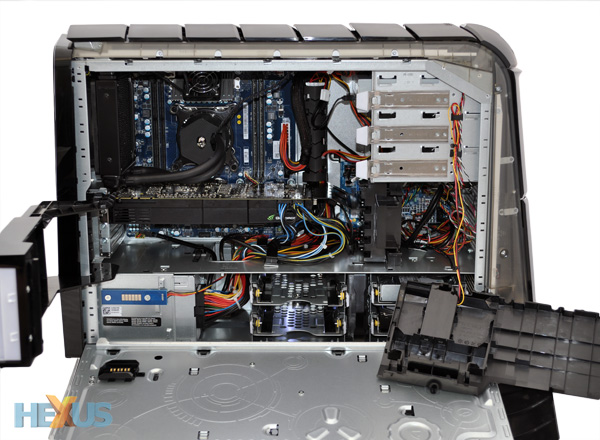
the image above shows the power supply, (hidden by a side cover) all the extra cables are hidden there and should be easily accessible.
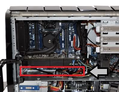

The image above shows a 2 connector pins for power in the green zone. When you take out GTX 560 Ti power connectors and place inside 690 GTX you need to add additional power connectors 2-pin.
PS, you might be able to find 8 connectors there though.
Good luck
-
Cooling system Alienware Aurora R4
Due to several accidents on my R4 Aurora, I google after the reason because these crashes, and I read that a problem could not work liquid cooling system. I live in Zurich in Switzerland, where I can buy a new cooling system?
eBay Europe... examples of US stock cooler ... 'none' wide wide 120x25mm or 120x38mm should be ok... Google images Corsair H80i

replace the stock R4 Alienware Aurora CPU cooling pump

R4 premium 38mm large radiator manufacturer 01YGW (google/bing/eBay or Dell Sales)
The thermal high quality grease if your cooler is delivered without any substantive multi-orientation
-
Aurora-R4, maximum hardware upgrades
Dear all
Currently I plan to update my beautiful Alienware Aurora R4 I bought at the beginning 2013
These are my current features:
OS: 8.1 64-bit Windows
CPU: Intel Core i7 3820 @ 3.60 GHz Sandy Bridge
Motherboard: Alienware 07JNH0 BIOS A11
Graphics card: NVIDIA GeForce GTX 680 2047 MB
RAM: 16.0 GB DDR3 800 MHz (11-11-11-28)
PSU: Alienware slandered 875 Watts.
-------------------------------------------------------------------------------------------------------------------------------------------
And here's what I plan to buy:
Corre CPU: Intel i7-4960 X processor Extreme Edition (15 M Cache, up to 4.00 GHz) Ivy Bridge.
Graphics card: Nvidia GeForce GTX Titan Z 12 GB.
RAM: Kingston Technology HyperX silly series 32 GB Kit (4X8Go) 1866 MHz DDR3 PC3-14900 CL10 XMP.
Any help with this list and what are your recommendations?
If Santa lays it under your tree this year, I would say that your R4 will be pleasantly maxed out. There are a couple of R4 on eBay w / this program installation, your list seems naughty & nice.


Above is a screen Aug22, just before dawn leaves the stage left: Titan Z is an approved card
- Note that this is a triple-slot card
You have a pair of video power supply cables, make sure that both get used on your map:
- What should I get my alienware aurora r4 to run a nvidia gtx 690
- http://en.community.Dell.com/Owners-Club/Alienware/f/3746/t/19497984
Fan / cooling upgrade advice:
- How to get my Alienware Aurora to run cooler r3
- http://en.community.Dell.com/Owners-Club/Alienware/f/3746/t/19607275
$ x 4960
- MicroCenter / USA them had just @ $800 new / sold out: http://www.microcenter.com/product/418178/Core_i7-4960X_36_GHz_LGA_2011_Boxed_Processor
- $980 new: http://www.superbiiz.com/detail.php?p=I7-4960XBX&c=fr&pid=40619e0838454c85724e07e717c762646946dea643ec3e2d5c56a83b5553728e&gclid=CJ6SxbLnnsICFXES7Aodf1kAFg
- These guys will prob'ly bite @ offer $700 - $725, 30 day warranty:
- http://www.eBay.com/ITM/CPU-Intel-Core-I7-4960X-socket-2011-extreme-processor-SR1AS-/111486275869?PT=LH_DefaultDomain_0&hash=item19f519911d
- wait for a holiday sale, as they are about $1,000 or release of January for the older stock
- 4930 k--> good compromise cpu<-- try="" to bag="" one="" @ $500="" or="" less="">
- 4820 good R4 upgrade cpu @ $250 k - $300 new
-
Map search mother Alienware Aurora R1
I got an Alienware Aurora R1 of the customer who was preparing to throw, as his son is off to College. Unfortunately I could not any background on his current condition.
So he came without hard drives or memory. I was able to recover 6 2 GB memory cards and place a spare inside sata drive before trying to start it.
When it turns on I get 3 beeps and a pause and 3 beeps again. He continues to cycle in this model. No video at all on any of the two video cards dual monitor.
My research indicates the beep code of 3 beeps means it needs a new motherboard.
I want to just restore this computer and give to some children. Cost isn't a factor.
Any help would be appreciated.
2 computer Alienware - General hardware troubleshooting
for those who do not know the beep code table:
Laptops
1 map of possible mother (covers BIOS corruption or ROM error)
2 no RAM detected
Possible motherboard 3 Chipset
4 (other) RAM failure
Stack 5 CMOS
6 video/chip
7 CPU
8 LCD
Desktop computers
1 map of possible mother (covers BIOS corruption or ROM error)
2 no RAM detected
Possible motherboard 3 Chipset
4 (other) RAM failure
5 real Time Clock (RTC)
6 video/chip
7 CPU


Maybe you are looking for
-
I just added Firefox to my Samsung Galaxy SII (GHS I757M). Best sites shows 4 iterations of Google. I want to change Top Sites. Is it possible to do this? Is there a way I can get rid of 3 Google references and get other sites? John OlsonOttawa, Cana
-
IE crashes after opening several sites...
Hello Thought I would add this problem to the mix. IE opens very well, but I get "inside" open several windows in a particular site, sometimes (usually) he'll eventually hang up IE and Windows tells me IE stopped working - even close the extra windo
-
Wireless hardware does not! Help!
I have a Compaq CQ58. Somehow my wireless does not work? I had a look on my computer (it is currently running windows 8.1), but he could not find a wireless device. It was running before wireless, but now he can't find the wireless lan device. All he
-
BDP-BX57 error 300 look a Netflix and no longer works
Hello. Everything is good until May 9, when my Blu - ray gives me a 300 error when viewing of Netflix.All other services are running.Firmware from Sony is the last: 11/02/2011 - if not recently changed.Powered off power and removed for 5 minutes and
-
replace a keyboard on a pavilion dv7 - 61213cl
I say several videos online to replace the keyboard for a laptop HP Pavilion, but can not find information for a Pavilion dv7 - 6123cl Entertainment PC. For that which never right on the back of this type of laptop is different than all the videos I