Alienware Aurora R4 doesn't start not
When I start the computer by pressing the power button, it loads the screen where it shows the version of the BIOS and stuff. After that, it goes to a loading screen, then it black screens. Please help someone, I'm not very good at such things. I posted a video, link below:
http://www.YouTube.com/watch?v=IyviMZ5mz20
Safe mode is F8 or this:
http://Windows.Microsoft.com/en-us/Windows-8/Windows-startup-settings-including-safe-mode
Diagnosis (PSA/ePSA) must come from a F12 boot menu.
Tags: Dell Products
Similar Questions
-
Facebook App doesn't start not
Hi all
I have a problem with the Facebook app for my TouchPad - it starts only once or twice and then it won't start more.
Looks like the works still features related to the account (photos etc), just the app itself that won't start.
I have already tried:
Does not:
* Uninstall/reinstall
* Uninstall/reboot/reinstall
Works for a short period:
* Erase data (followed of re-registration/reinstall etc.)
* Inkwell (not tried it myself, but apparently works also for a little while)
Anyone else here with a TouchPad that knows these symptoms? Inkwell/deletion is not a solution because the I have to redo _tout_.
I don't know if they fixed the issue directly or if it was because of another bug, but after the 3.0.2 update the Facebook app now starts with my regional setting

-
CS6 download indicator doesn't start not
Download CS6 didn't start there at - it a problem with the download site?
Download assistant seems to wait for the download to start
found it... to save to the desktop, not a program folder. started to download
-
Process scheduler doesn't start not
Hello
I am running 9.1 PeopleSoft HR, db Oracle 11.1.0.6, PT 8.50. The database, the application server and the web server are all on the same machine - Enterprise Linux 5.
Basically, I have problems to start the server after an ip address change.
I changed the system wide configuration ip - / etc/hosts, network ifcfg-eth0 script and so forth
psappsrv.cfg has changed with the new corresponding, in charge of the tuxconfig edited ip address
(also changed the configuration.properties for PIA)
As far as the network is concerned, everything works fine - LAN and outdoor access.
The database server and the Application starts ok. I can connect using sqlplus he-based and the Application Server starts without errors of psadmin.
When I try to start the Scheduler process I get the following:
CRP / < domain >/LOGS/stderr:Starting Process Scheduler Server PSUNX for Database HDEMO91 ... Booting all admin and server processes in /root/psft/pt/8.50/appserv/prcs/HDEMO91/PSTUXCFG INFO: Oracle Tuxedo, Version 10.3.0.0, 64-bit, Patch Level (none) Booting admin processes ... exec BBL -A : process id=5200 ... Started. Booting server processes ... exec PSMSTPRC -o ./LOGS/stdout -e ./LOGS/stderr -A -- -CD HDEMO91 -PS PSUNX -A start -S PSMSTPRC : process id=5201 ... Started. exec PSAESRV -o ./LOGS/stdout -e ./LOGS/stderr -- -CD HDEMO91 -S PSAESRV : process id=5221 ... Started. exec PSAESRV -o ./LOGS/stdout -e ./LOGS/stderr -- -CD HDEMO91 -S PSAESRV : process id=5229 ... Started. exec PSAESRV -o ./LOGS/stdout -e ./LOGS/stderr -- -CD HDEMO91 -S PSAESRV : process id=5237 ... Started. exec PSDSTSRV -o ./LOGS/stdout -e ./LOGS/stderr -p 1,600:1,1 -sPostReport -- -CD HDEMO91 -PS PSUNX -A start -S PSDSTSRV : CMDTUX_CAT:1685: ERROR: Application initialization failure tmboot: CMDTUX_CAT:827: ERROR: Fatal error encountered; initiating user error handler exec tmshutdown -y
CRP / < domain >/LOGS/stdout:PSJNI: INFO: Unloaded the Java VM
Now, looking at the stdout, it seems that the solution may be a simple configuration change, but how do I access a report node page?=================================Error=============================== Message: The FTP Address for transferring files to the Report Repository is not specified Please correct this error by updating the info for Report Node: ReportNode in the Process Scheduler Manager's Report Node Definition page. Due to this error, the Process Scheduler Server will not be started.. Please correct this error prior to attempting to start the server PSUNX. =====================================================================
I tried to start PIA just to see what would happen. I get the following message on the page of signon PS:
I'm a newbie at this and appreciate any input.CHECK APPSERVER LOGS. THE SITE BOOTED WITH INTERNAL DEFAULT SETTINGS, BECAUSE OF: bea.jolt.ServiceException: Invalid Session
Kind regards.Honza,
Server Web fails to communicate with appserver. I guess that the port number you have given to the webserver configuration files (configuration.properties) is correct? Check psappsrv.cfg and match the port numbers.
1. try changing IP address host name of the Web configuration.properties file server. Server Web Bounce (Restart) and appserver. If this does not
2 recreating the field appserver and Web server with a different port number other than 9000. Make sure that the port numbers are not blocked-Vijay
-
When I turn it on it says SanDisk and then the screen becomes white and SanDisk and then again over and over. I put in recovery mode and downloaded the firmware again, but it still does the same thing. Any ideas?
In recovery DO NOT FORMATER 16 MB partition mode
Create a folder called "Sansa.fmt" and put on the partition - disconnect the Sansa to the computer and allow it to restart.
This file being present tells the Sansa format itself, you WILL LOSE all your music, photos, videos (copy them to your computer before we do this!)
See if that fixes it.
-
Install testversion InDesign, the download doesn't start not
Hi, I am installing InDesign testversion. When I klick on install nothing happens it just says download. I have a Macbook OSx Version 10.9.5 (2010) and Yosemite is installed. Any ideas? Thank you
Hello
Please try to download the application directly via the link below:
Direct download links of Adobe CC 2015: 2015 creative cloud release | ProDesignTools
Kind regards
Sheena
-
Alienware Aurora r4 does not start with new graphics card.
Hey,.
I have an alienware aurora end of 2012 I believe.
I currently have a series of 6800 AMD raedon graphics card, processor 3930 r9 k i7 and 8 GB of ram.
I recently bought a MSI gtx 970 game to replace my old graphics card. I plug this card and it even lights up when I turn on the computer, but however my pc only happens to the start screen where I get the choice after pressing F2 and F12 and then freezes and I can't do anything. I then hear 3 beeps of inside my pc and then it proceeds to a blackscreen where my only choice is to turn it off manually.
I tried to uppgrade my BIOS without much success (dident make it work), uninstall all graphics drivers from AMD, but nothing has changed.
So I'm clueless I'm kinda a noob of the pc and have no idea what could cause this and would love help to explain what happens if all goes well if anyone knows a fix.
THX in advance :)
You you connected all power cables required PCIe 970? They are probably different config as AMD-6800. You should have 875w PS, but you might need to check that.
Probably should have uninstalled AMD Driver Suite (catalyst) before removing the card from AMD.
If card MSI BIOS a double switch, you can try another position.
Try Mode Windows safe.
What operating system do you use? Are you running the UEFI BIOS or legacy Mode?
-
Alienware Aurora ALX lights does not work master of e/s part #.
I tried to get the lights on my Alienware Aurora ALX job. The only lights that works are the head alien and the flange. Work, I mean that they are white. When I Command Center, it doesn't even show fan/readings of temperature or light speeds. I think that my I/o card is bad.
I can not get something to change in Comand Center.
I tried all the solutions on the forums and nothing seems to work.
I reinstalled windows 3 times. Nothing.
I reinstalled Alienware Command Center 6 times (correct version and the different)
I tried shutting down the computer, unplug the power cord and hold the power button for 1-2 minutes thing, didn't work.
I went to reset the map using the Green rider, did not work.
I ran a diagnosis and everything seems fine, don't know if it's testing the Master Control I/O Board.
I'll order an Alienware Aurora ALX Alien FX / Master Control I/O Board, because I am sure that my i/o board is bad.
The reference is 02JXP2 and version 1.1 mine said A02
The white mark on my map of IO said A02, but it has the same part number 02JXP2 and version 1.1.
My question is can I use a Board with the same part number but it says A04?
Here is a picture of the map of IO with the A02, I want to buy a economy part number 02JXP2 and at the bottom says A04 instead, but is a version 1.1.
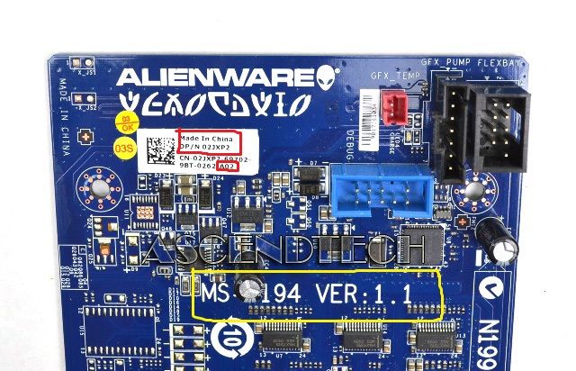
If anyone as any advice before ordering the card / advice to see if I can get the lights work on my computer?
ThatOne_GamerI don't have the cable that connects the motherboard to the MIO card.
I'm sure that's why my ect lights do not work.
Right... If it is not connected, it cannot work.
-
(Redirected) Is it bad start for Alienware Aurora R4 (UEFI, legacy) mode?
Recently, I made the stupid mistake of updating my bios as bios 5 to 12 because I get a new graphics card soon and heard that you must update the bios first. As planned, it was wrong and it crashed when rebooting and all-day was stuck at a black screen when starting my PC saying to choose the priority of seed or something.
Finally, I tried everything to do in F12 menu, I decided to spend the boot mode in the UEFI to legacy. He actually began after doing this and luckily my hard drive is intact, but he had some interesting things that I noticed. First of all, my HARD disk space seems to decrease slightly as I realized to my PC. Second, there was weird stuff with Alien Autopsy (not really, but it has an error message). Also it could run a little bit slower. Hard to say. It starts more slowly as well. Then, change the dangerous startup parameters, or I made the right choice? Or I just ruin my PC today?
I have an Alienware Aurora R4 running any Windows 7.
Better in this position in the Alienware owners Club Forum, here:
http://en.community.Dell.com/Owners-Club/Alienware/default.aspx
Bev.
-
A start-up ware Alienware Aurora ALX
I bought an Alienware Aurora earlier this spring and have noticed that it takes a long time to start. From the time I hit my power button, until all the icons on my screen are visible and able to work, it takes anywhere from 7 to 9 minutes.
I can see my desktop in 3-5 minutes, but due to other processes that I can click on Firefox and nothing won't happen for a few more minutes.
When I bought this computer I went with the RAID 0 option. I had called and told them I wanted an SSD and a different option of RAID, but was told they don't do that. So, I stuck with the RAID 0 option. But have always noticed the slow start has been. What is indigestion of alienware, like thermal controls? Or something else that makes it so slow?
I do not support RAID on desktop computers, but it degraded sounds or something.
IMHO, I'd install SSD 256 GB (or more)... Although I had to clean install. My computer starts (for usable desktop) in about 20 seconds (with 100 process running).
http://en.community.Dell.com/Owners-Club/Alienware/f/3746/t/19568143
Then I would probably break the raid, use a spinner HDD for large game installs and one for data files.
-
Problem starting r4 Alienware Aurora ALX
My Aurora ALX R4 doesn't start, the GET really loud fan and nothing happens. Sometimes it restarts the process. I need help badly
Yes, this seems to be the serial number - please go ahead and delete your post...
This is sensitive information
And Yes. the PCI shroud covers the CMOS battery. Try to do this first.
-
How to reinstall a Windows 8 dell alienware aurora r4 to factory settings?
A friend of mine had his PC scammed (guy calls, said you that they are Microsoft and you are infected, enter your PC and then you lock out and ask $ money to let you back in).
Anyway, he has a PC Dell Alienware Aurora R4 (comes with) running Windows 8 or 8.1 - I don't know but I know that he has not improved/changed anything. The system came with a DVD resource (nothing else).
Now all we want to do is to restore factory default, there is nothing about this of any importance to save...
I looked on the internet and found what looks like the right solution:
-Enter advanced service options (holding shift at the start), select "troubleshooting."
> "Icon Dell Backup and Recovery" is missing (how could it be?Without that, I'm totally stuck...
Any suggestions? Recommendations? Ideas?Thank you
After that a clean installation of Windows and the drivers of Dell system, Dell backup and restoration facility will create a new recovery partition of your own installation that you can restore as new factory settings.
-
Need help upgrading my alienware aurora
Here are all the technical features of cpu - z, keeping in mind both the original production (HD5670x2 crossfire) doesn't have a video card, I currently installed I picked up to 49.99 (half price) I was looking in the privateer, unit cooling, but even under the huge load, my computer runs at 27 c so... I have 12 GB memory, I want to game time to load faster... can I switch the processor without having to tear the entire computer? Maybe just the PSU and CPU? the cpu is removable for a best i7? that would help? cause I'm sure that the 12 GB of memory is not in desperate need of good memory? IM xcom2 to play and wait a good 2-3 minutes between the levels on the loading time... Anyway here is the screenshots, and below that is the cpu - z text file

TXT of CPU - Z report
-------------------------------------------------------------------------Binary files
-------------------------------------------------------------------------CPU - Z version 1.76.0.x64
Processors
-------------------------------------------------------------------------Number of processors 1
Number of threads 8APICs
-------------------------------------------------------------------------Processor 0
-Core 0
-Wire 0 0
-Thread 1 1
-Core 1
-0-2 wire
-Wire 1 3
-Core 2
-0-4 wire
-Wire 5 1
-Core 3
-0-6 wire
-Wire 1 7Timers
-------------------------------------------------------------------------Timer ACPI 3,580 MHz
Timer HPET 14,318 MHz
Timer perf 2,741 MHz
Sys 1,000 KHz timerInformation for processors
-------------------------------------------------------------------------Processor 1 ID = 0
Number of hearts 4 (max 8)
The number of threads 8 (max 16)
Name Intel Core i7 930
Codename Bloomfield
Specification Intel (r) Core i7 CPU 930 @ 2.80GHz
Package (platform ID) Socket 1366 LGA (0 x 1)
CPUID 6.A.5
CPUID extended 6. 1A
Core Stepping D0
The 45 nm technology
TDP limit 130.0 Watts
Basic speed 2940,5 MHz
Multiplier x Bus 22,0 x 133,7 MHz speed
2405,9 MHz rated Bus speed
Stock frequency of 2800 MHz
Instructions sets MMX, SSE, SSE2, SSE3, SSSE3, SSE4.1, SSE4.2, EM64T, VT - x
Data L1 cache 4 x 32 KB, size 8-way line set associative, 64 bytes
L1 instruction cache 4 x 32 KB, size 4-way set associative line, 64 bytes
L2 cache 4 x 256 KB, size 8-way line set associative, 64 bytes
Cache 8 MB L3, size 16-way set associative line, 64 bytes
FID/VID control YesTurbo Mode supported, enabled
3066 MHz Max turbo frequency
Max-non-Turbo report 21 x
Max turbo report 23 x
Max efficiency report 12 x
TDC limited 110 amps
Number of bus max 255
PCI peripheral device connected to the 255 bus, device 2, function 0
PCI peripheral device connected to the 255 bus, device 3, function 4Temperature 0 57 ° C (134 ° F) [0x2B] (Core #0)
Power supply 0 40.52 W (package)Thread dumps
-------------------------------------------------------------------------CPU thread 0
APIC ID 0
Topology Processor ID 0, Core ID 0, Thread ID 0
Type 01020001:
0000000Bh Max CPUID level
Level of position Max CPUID 80000008 h
Descriptor level 1, D, 32 KB, 2 wire (s) cache
Descriptor level 1, I, 32 k, 2 wire (s) cache
Descriptor cache level 2, U, 256 KB, 2 wire (s)
Descriptor cache level 3, U, 8 MB, 16 threadsCPUID
0 x 00000000 0x0000000B 0x756E6547 0x6C65746E 0x49656E69
0 x 00000001 0x000106A5 0 x 03100800 0x0098E3BD 0xBFEBFBFF
0 x 00000002 0x55035A01 0x00F0B2E4 0 x 00000000 0x09CA212C
0 x 00000003 0x00000000 0x00000000 0x00000000 0x00000000
0 x 00000004 0x0000003F 0x01C0003F 0x1C004121 0x00000000
0 x 00000004 0x1C004122 0x00C0003F 0x0000007F 0x00000000
0 x 00000004 0x1C004143 0x01C0003F 0x000001FF 0x00000000
0 x 00000004 0x1C03C163 0x03C0003F 0x00001FFF 0x00000002
0x00000005 00000040 0 x 0 x 00000040 0 x 00000003 0 x 00001120
0 x 00000006 0 x 00000003 0x00000002 0x00000001 0x00000000
0 x 00000007 0x00000000 0x00000000 0x00000000 0x00000000
0x00000008 0x00000000 0x00000000 0x00000000 0x00000000
0 x 00000009 0x00000000 0x00000000 0x00000000 0x00000000
0x0000000A 0 x 07300403 0 x 00000044 0x00000000 0 x 00000603
0x0000000B 0x00000001 0x00000002 0x00000100 0 x 00000003
0x0000000B 0 x 00000004 0x00000008 0 x 00000201 0 x 00000003
0x80000000 0 x 80000008 0x00000000 0x00000000 0x00000000
0 x 80000001 0x00000000 0x00000000 0x00000001 0 x 28100800
0 x 80000002 0x65746E49 0x2952286C 0x726F4320 0x4D542865
0 x 80000003 0 x 37692029 0 x 55504320 20202020 0 x 0 x 20202020
0 x 80000004 0 x 30333920 0 x 20402020 0x30382E32 0x007A4847
0 x 80000005 0x00000000 0x00000000 0x00000000 0x00000000
0 x 80000006 0x00000000 0x00000000 0 x 01006040 0x00000000
0 x 80000007 0x00000000 0x00000000 0x00000000 0x00000100
0 x 80000008 0 x 00003024 0x00000000 0x00000000 0x00000000MSR 0X0000001B, 0X00000000 0XFEE00900
MSR 0X0000003A 0X00000000 0X00000005
MSR 0X000001A0 0X00000000 0 X 00850089
MSR 0X000000CE 0X00000C00 0 X 00011501
MSR 0 X 00000017 0X00040000 0X00000000
MSR 0 X 00000035 0X00000000 0 X 00040008
MSR 0X000000C1 0X00000000 0X00000000
MSR 0X000000C2 0X00000000 0X00000000
MSR 0X000000C3 0X00000000 0X00000000
MSR 0X000000C4 0X00000000 0X00000000
MSR X 0 00000186 0X00000000 0X00000000
MSR X 0 00000187 0X00000000 0X00000000
MSR 0X000001AD 0X00000000 0 X 16161617
MSR 0X0000019A 0X00000000 0X00000000
MSR 0X000001A4 0X00000000 0X00000000
MSR 0X000001AC 0X00000000 0 X 03700410
MSR 0X000001FC 0X00000000 0X00000002
MSR 0 X 00000300 0X00000000 0XE0000001
MSR 0X0000019C 0X00000000 0X882B0000
MSR 0X000001A2 0X00000000 0 X 00641400
MSR 0XC0000103 0X00000000 0X00000000
MSR X 0 00000198 0X00000000 0 X 00000016
MSR X 0 00000199 0X00000000 0 X 00000016Chipset
-------------------------------------------------------------------------Northbridge Intel X 58 Rev.. 13
Southbridge Intel 82801IR (ICH10R) Rev. 00
Graphics interface PCI-Express
Width link PCI-E x 16
PCI-E Max Link width x 16
Type of DDR3 memory
Memory size 12 GB
Channel Triple
Frequency 668,3 MHz memory (02:10)
Latency CASE # (CL) 9.0
# For CASE # delay (tRCD) RAS 9
RAS # Precharge (tRP) 9
Cycle Time (tRAS) 24
Time to Row Refresh Cycle (tRFC) 74
Control rate (CR) 2 t
Uncore frequency 2673,2 MHz
Host Bridge 0 x 3405
Host Bridge 0x2C41
Host Bridge 0x2C01
Host Bridge 0x2C10
Host Bridge 0x2C11
Host Bridge 0x2C18
Host Bridge 0x2C19
Host Bridge 0x2C1C
Host Bridge 0x2C20
Host Bridge 0x2C21
Host Bridge 0x2C22
Host Bridge 0x2C23
Host Bridge 0x2C28
Host Bridge 0x2C29
Host Bridge 0x2C2A
Host Bridge 0x2C2B
Host Bridge 0x2C30
Host Bridge 0x2C31
Host Bridge 0x2C32
Host Bridge 0x2C33Memory SPD
-------------------------------------------------------------------------DIMM # 1
SMBus address 0 x 50
Type of DDR3 memory
UDIMM module format
Manufacturer (ID) Nanya Technology (7F7F7F0B000000000000)
Size 2048 MB
Bandwidth Max PC3-10700 (667 MHz)
NT2GC64B8HC0NF-CG part number
Serial number 085A 2264
Date week 51/year 10 manufacturing
Number of banks 8
Nominal voltage 1.50 Volts
EPP no
XMP no
AMP no
Timings JEDEC CL-tRCD-tRP-tRAS-tRC table @ frequency
JEDEC #1 6.0 - 6-6-17-23 @ 457 MHz
JEDEC #2 7.0 - 7-7-20-27 @ 533 MHz
JEDEC #3 8.0 - 8-8-22-30 MHz 609
JEDEC #4 9.0 - 9-9-24-33 @ 666 MHzDIMM # 2
SMBus address 0 x 51
Type of DDR3 memory
UDIMM module format
Manufacturer (ID) Nanya Technology (7F7F7F0B000000000000)
Size 2048 MB
Bandwidth Max PC3-10700 (667 MHz)
NT2GC64B8HC0NF-CG part number
Serial number D7592264
Date week 51/year 10 manufacturing
Number of banks 8
Nominal voltage 1.50 Volts
EPP no
XMP no
AMP no
Timings JEDEC CL-tRCD-tRP-tRAS-tRC table @ frequency
JEDEC #1 6.0 - 6-6-17-23 @ 457 MHz
JEDEC #2 7.0 - 7-7-20-27 @ 533 MHz
JEDEC #3 8.0 - 8-8-22-30 MHz 609
JEDEC #4 9.0 - 9-9-24-33 @ 666 MHzDIMM # 3
SMBus address 0 x 52
Type of DDR3 memory
UDIMM module format
Manufacturer (ID) Nanya Technology (7F7F7F0B000000000000)
Size 2048 MB
Bandwidth Max PC3-10700 (667 MHz)
NT2GC64B8HC0NF-CG part number
Serial number 085A 2262
Date week 51/year 10 manufacturing
Number of banks 8
Nominal voltage 1.50 Volts
EPP no
XMP no
AMP no
Timings JEDEC CL-tRCD-tRP-tRAS-tRC table @ frequency
JEDEC #1 6.0 - 6-6-17-23 @ 457 MHz
JEDEC #2 7.0 - 7-7-20-27 @ 533 MHz
JEDEC #3 8.0 - 8-8-22-30 MHz 609
JEDEC #4 9.0 - 9-9-24-33 @ 666 MHzDIMM # 4
SMBus address 0 x 53
Type of DDR3 memory
UDIMM module format
Manufacturer (ID) Nanya Technology (7F7F7F0B000000000000)
Size 2048 MB
Bandwidth Max PC3-10700 (667 MHz)
NT2GC64B8HC0NF-CG part number
Serial number 085A 2261
Date week 51/year 10 manufacturing
Number of banks 8
Nominal voltage 1.50 Volts
EPP no
XMP no
AMP no
Timings JEDEC CL-tRCD-tRP-tRAS-tRC table @ frequency
JEDEC #1 6.0 - 6-6-17-23 @ 457 MHz
JEDEC #2 7.0 - 7-7-20-27 @ 533 MHz
JEDEC #3 8.0 - 8-8-22-30 MHz 609
JEDEC #4 9.0 - 9-9-24-33 @ 666 MHzDIMM # 5
SMBus address 0 x 54
Type of DDR3 memory
UDIMM module format
Manufacturer (ID) Nanya Technology (7F7F7F0B000000000000)
Size 2048 MB
Bandwidth Max PC3-10700 (667 MHz)
NT2GC64B8HC0NF-CG part number
Serial number 36582262
Date week 51/year 10 manufacturing
Number of banks 8
Nominal voltage 1.50 Volts
EPP no
XMP no
AMP no
Timings JEDEC CL-tRCD-tRP-tRAS-tRC table @ frequency
JEDEC #1 6.0 - 6-6-17-23 @ 457 MHz
JEDEC #2 7.0 - 7-7-20-27 @ 533 MHz
JEDEC #3 8.0 - 8-8-22-30 MHz 609
JEDEC #4 9.0 - 9-9-24-33 @ 666 MHzDIMM # 6
SMBus address 0 x 55
Type of DDR3 memory
UDIMM module format
Manufacturer (ID) Nanya Technology (7F7F7F0B000000000000)
Size 2048 MB
Bandwidth Max PC3-10700 (667 MHz)
NT2GC64B8HC0NF-CG part number
Serial number 085A 2263
Date week 51/year 10 manufacturing
Number of banks 8
Nominal voltage 1.50 Volts
EPP no
XMP no
AMP no
Timings JEDEC CL-tRCD-tRP-tRAS-tRC table @ frequency
JEDEC #1 6.0 - 6-6-17-23 @ 457 MHz
JEDEC #2 7.0 - 7-7-20-27 @ 533 MHz
JEDEC #3 8.0 - 8-8-22-30 MHz 609
JEDEC #4 9.0 - 9-9-24-33 @ 666 MHzDIMM # 1
Registers SPD
00 01 02 03 04 05 06 07 08 09 0 HAS 0B 0E 0F 0D 0C
00 92 10 0 B 02 02 11 00 09 03 52 01 08 00 00 3 0C
10 69 78 69 30 69 11 20 89 70 03 3 3 00 F0 82 05
20 00 00 00 00 00 00 00 00 00 00 00 00 00 00 00 00
30 00 00 00 00 00 00 00 00 00 00 00 00 0F 11 01 01
40 00 00 00 00 00 00 00 00 00 00 00 00 00 00 00 00
50 00 00 00 00 00 00 00 00 00 00 00 00 00 00 00 00
60 00 00 00 00 00 00 00 00 00 00 00 00 00 00 00 00
70 00 00 00 00 00 83 0B 0D 10 51 08 5 A 22 64 AND 06 A1
4TH 4TH 80 54 32 47 43 36 34 42 38 48 43 30 46 2D 43
90 47 20 00 00 83 0 B 00 00 00 00 20 00 00 00 00 4
4 31 30 43 31 34 30 53 45 44 A0 4 54 30 35 31 36
B0 00 00 00 00 00 00 00 00 00 00 00 00 00 00 00 00
C0 00 00 00 00 00 00 00 00 00 00 00 00 00 00 00 00
D0 00 00 00 00 00 00 00 00 00 00 00 00 00 00 00 00
E0 00 00 00 00 00 00 00 00 00 00 00 00 00 00 00 00
F0 00 00 00 00 00 00 00 00 00 00 00 00 00 00 00 00DIMM # 2
Registers SPD
00 01 02 03 04 05 06 07 08 09 0 HAS 0B 0E 0F 0D 0C
00 92 10 0 B 02 02 11 00 09 03 52 01 08 00 00 3 0C
10 69 78 69 30 69 11 20 89 70 03 3 3 00 F0 82 05
20 00 00 00 00 00 00 00 00 00 00 00 00 00 00 00 00
30 00 00 00 00 00 00 00 00 00 00 00 00 0F 11 01 01
40 00 00 00 00 00 00 00 00 00 00 00 00 00 00 00 00
50 00 00 00 00 00 00 00 00 00 00 00 00 00 00 00 00
60 00 00 00 00 00 00 00 00 00 00 00 00 00 00 00 00
70 00 00 00 00 00 83 0B 0D 10 51 59 22 64 06 A1 D7
4TH 4TH 80 54 32 47 43 36 34 42 38 48 43 30 46 2D 43
90 47 20 00 00 83 0 B 00 00 00 00 20 00 00 00 00 4
4 31 30 43 31 34 30 53 45 44 A0 4 54 30 35 31 36
B0 00 00 00 00 00 00 00 00 00 00 00 00 00 00 00 00
C0 00 00 00 00 00 00 00 00 00 00 00 00 00 00 00 00
D0 00 00 00 00 00 00 00 00 00 00 00 00 00 00 00 00
E0 00 00 00 00 00 00 00 00 00 00 00 00 00 00 00 00
F0 00 00 00 00 00 00 00 00 00 00 00 00 00 00 00 00DIMM # 3
Registers SPD
00 01 02 03 04 05 06 07 08 09 0 HAS 0B 0E 0F 0D 0C
00 92 10 0 B 02 02 11 00 09 03 52 01 08 00 00 3 0C
10 69 78 69 30 69 11 20 89 70 03 3 3 00 F0 82 05
20 00 00 00 00 00 00 00 00 00 00 00 00 00 00 00 00
30 00 00 00 00 00 00 00 00 00 00 00 00 0F 11 01 01
40 00 00 00 00 00 00 00 00 00 00 00 00 00 00 00 00
50 00 00 00 00 00 00 00 00 00 00 00 00 00 00 00 00
60 00 00 00 00 00 00 00 00 00 00 00 00 00 00 00 00
70 00 00 00 00 00 83 0B 0D 10 51 08 5 A 22 62 AND 06 A1
4TH 4TH 80 54 32 47 43 36 34 42 38 48 43 30 46 2D 43
90 47 20 00 00 83 0 B 00 00 00 00 20 00 00 00 00 4
4 31 30 43 31 34 30 53 45 44 A0 4 54 30 35 31 36
B0 00 00 00 00 00 00 00 00 00 00 00 00 00 00 00 00
C0 00 00 00 00 00 00 00 00 00 00 00 00 00 00 00 00
D0 00 00 00 00 00 00 00 00 00 00 00 00 00 00 00 00
E0 00 00 00 00 00 00 00 00 00 00 00 00 00 00 00 00
F0 00 00 00 00 00 00 00 00 00 00 00 00 00 00 00 00DIMM # 4
Registers SPD
00 01 02 03 04 05 06 07 08 09 0 HAS 0B 0E 0F 0D 0C
00 92 10 0 B 02 02 11 00 09 03 52 01 08 00 00 3 0C
10 69 78 69 30 69 11 20 89 70 03 3 3 00 F0 82 05
20 00 00 00 00 00 00 00 00 00 00 00 00 00 00 00 00
30 00 00 00 00 00 00 00 00 00 00 00 00 0F 11 01 01
40 00 00 00 00 00 00 00 00 00 00 00 00 00 00 00 00
50 00 00 00 00 00 00 00 00 00 00 00 00 00 00 00 00
60 00 00 00 00 00 00 00 00 00 00 00 00 00 00 00 00
70 00 00 00 00 00 83 0B 0D 10 51 08 5 A 22 61 AND 06 A1
4TH 4TH 80 54 32 47 43 36 34 42 38 48 43 30 46 2D 43
90 47 20 00 00 83 0 B 00 00 00 00 20 00 00 00 00 4
4 31 30 43 31 34 30 53 45 44 A0 4 54 30 35 31 36
B0 00 00 00 00 00 00 00 00 00 00 00 00 00 00 00 00
C0 00 00 00 00 00 00 00 00 00 00 00 00 00 00 00 00
D0 00 00 00 00 00 00 00 00 00 00 00 00 00 00 00 00
E0 00 00 00 00 00 00 00 00 00 00 00 00 00 00 00 00
F0 00 00 00 00 00 00 00 00 00 00 00 00 00 00 00 00DIMM # 5
Registers SPD
00 01 02 03 04 05 06 07 08 09 0 HAS 0B 0E 0F 0D 0C
00 92 10 0 B 02 02 11 00 09 03 52 01 08 00 00 3 0C
10 69 78 69 30 69 11 20 89 70 03 3 3 00 F0 82 05
20 00 00 00 00 00 00 00 00 00 00 00 00 00 00 00 00
30 00 00 00 00 00 00 00 00 00 00 00 00 0F 11 01 01
40 00 00 00 00 00 00 00 00 00 00 00 00 00 00 00 00
50 00 00 00 00 00 00 00 00 00 00 00 00 00 00 00 00
60 00 00 00 00 00 00 00 00 00 00 00 00 00 00 00 00
70 00 00 00 00 00 83 0B 10 51 36 58 22 62 06 A1 0D
4TH 4TH 80 54 32 47 43 36 34 42 38 48 43 30 46 2D 43
90 47 20 00 00 83 0 B 00 00 00 00 20 00 00 00 00 4
4 31 30 43 31 34 30 53 45 44 A0 4 54 30 35 31 36
B0 00 00 00 00 00 00 00 00 00 00 00 00 00 00 00 00
C0 00 00 00 00 00 00 00 00 00 00 00 00 00 00 00 00
D0 00 00 00 00 00 00 00 00 00 00 00 00 00 00 00 00
E0 00 00 00 00 00 00 00 00 00 00 00 00 00 00 00 00
F0 00 00 00 00 00 00 00 00 00 00 00 00 00 00 00 00DIMM # 6
Registers SPD
00 01 02 03 04 05 06 07 08 09 0 HAS 0B 0E 0F 0D 0C
00 92 10 0 B 02 02 11 00 09 03 52 01 08 00 00 3 0C
10 69 78 69 30 69 11 20 89 70 03 3 3 00 F0 82 05
20 00 00 00 00 00 00 00 00 00 00 00 00 00 00 00 00
30 00 00 00 00 00 00 00 00 00 00 00 00 0F 11 01 01
40 00 00 00 00 00 00 00 00 00 00 00 00 00 00 00 00
50 00 00 00 00 00 00 00 00 00 00 00 00 00 00 00 00
60 00 00 00 00 00 00 00 00 00 00 00 00 00 00 00 00
70 00 00 00 00 00 83 0B 0D 10 51 08 5 A 22 63 AND 06 A1
4TH 4TH 80 54 32 47 43 36 34 42 38 48 43 30 46 2D 43
90 47 20 00 00 83 0 B 00 00 00 00 20 00 00 00 00 4
4 31 30 43 31 34 30 53 45 44 A0 4 54 30 35 31 36
B0 00 00 00 00 00 00 00 00 00 00 00 00 00 00 00 00
C0 00 00 00 00 00 00 00 00 00 00 00 00 00 00 00 00
D0 00 00 00 00 00 00 00 00 00 00 00 00 00 00 00 00
E0 00 00 00 00 00 00 00 00 00 00 00 00 00 00 00 00
F0 00 00 00 00 00 00 00 00 00 00 00 00 00 00 00 00Monitoring
-------------------------------------------------------------------------Model of motherboard 04VWF2 (0 x 00000189 - 0x004D8240)
LPCIO
-------------------------------------------------------------------------LPCIO seller are
LPCIO model F71882F
LPCIO Vendor ID 0 x 1934
LPCIO Chip ID 0 x 541
0x4E config Mode i/o address
Configuration Mode NDA 0x4
Saves the configuration mode
00 01 02 03 04 05 06 07 08 09 0 HAS 0B 0E 0F 0D 0C
00 FF FF 00 FF FF FF FF FF 04 FF FF FF FF FF FF FF
10 FF FF FF FF FF FF FF FF FF FF FF FF FF FF FF FF
20 05 41 20 19 34 00 00 30 44 00 40 60 08 00 00 0F
30 01 FF FF FF FF FF FF FF FF FF FF FF FF FF FF FF
40 FF FF FF FF FF FF FF FF FF FF FF FF FF FF FF FF
50 FF FF FF FF FF FF FF FF FF FF FF FF FF FF FF FF
60 0 A 00 FF FF FF FF FF FF FF FF FF FF FF FF FF FF
70 00 FF FF FF FF FF FF FF FF FF FF FF FF FF FF FF
Register space LPC, base address = 0x0A00Hardware monitors
-------------------------------------------------------------------------Door F71882F hardware monitor
Voltage Volt 3.39 0 [0xD4] (+ 3, 3V)
Voltage Volt 1 1.24 [0x9B] (CPU VCORE)
Voltage Volt 2 2.05 [0x80] (VIN2)
Voltage Volt 3 1.21 [0 x 67] (VIN3)
Voltage Volt 4 5.05 0 x [78] (+ 5V)
Voltage Volt 5 12.14 [0x8A] (+ 12V)
Voltage 6 1.78 Volts [0x6F] (VIN6)
Voltage Volt 7 3.38 [0xD3] (VSB3V)
Voltage Volt 8 3.23 [0xCA] (VBAT)
Temperature 0 to 40 ° C (104 ° F) 0 x [28] (TMPIN0)
Temperature 1 59 ° C (138 ° F) [0x3B] (TMPIN1)
2 temperature of 53 ° C (127 ° F) 0 x [35] (TMPIN2)
Fan 0 1205 RPM [0x4DD] (FANIN0)
Fan PWM 0 100 pc [0xFF] (CPU)
Fan PWM 1 100 pc [0xFF] (System 1 fan)
Fan PWM 2 100 pc [0xFF] (System Fan 2)
Fan PWM 3 100 pc [0xFF] (3 system fan)
Register space LPC, base address = 0x0A0000 01 02 03 04 05 06 07 08 09 0 HAS 0B 0E 0F 0D 0C
FF 00 03 00 00 FF FF FF FF FF FF 01 00 55 4 00 00
10 00 00 00 00 FF FF FF FF FF FF FF FF FF FF FF FF
20 D4 5F 75 49 78 8 B 6F D3 CA FF FF FF FF FF FF FF
30 FF FF FF FF FF FF FF FF FF FF FF FF FF FF FF FF
40 FF FF FF FF FF FF FF FF FF FF FF FF FF FF FF FF
50 FF FF FF FF FF FF FF FF FF FF 03 04 10 19 34 FF
60 00 00 00 00 FF FF 00 00 00 00 FF 08 40 24 00 FF
70 FF FF FF 28 3 B FF 35 FF FF FF FF FF FF FF FF FF
80 FF FF FF FF FF FF FF FF FF FF FF FF FF FF A8 FF
90 00 0E 0E 00 16 00 FF FF 00 FF 24 01 02 55 FF 1 A
A0 DF 04 E0 01 4 48 3 A 34 00 09 17 28 58 1 2D 04D
B0 FF 05 03 FF 3 32 28 C 5 C 0F 1E 0 B 00 12 2 HAS IN THE 30 0E
C0 FF 05 03 FF 3 32 28 C 5 C 0F 1E 0 B 00 12 2 HAS IN THE 30 0F
D0 0F FF 05 03 FF 3 32 28 C 5 C 1 0 B 00 12 2 HAS IN THE 30 0F
E0 FF FF FF FF FF FF FF FF FF FF FF FF FF FF FF FF
F0 00 00 00 00 00 00 3 B FF 03 43 00 FF FF FF FF FFMonitor hardware NVIDIA NVAPI
Voltage Volt 0 0.98 [0x3CF] (VIN0)
Temperature 0 34 ° C (93 ° F) 0 x [22] (TMPIN0)
0 21 0 x [15] pc PWM fan (FANPWMIN0)
Clock speed 324.00 0 MHz [0 x 144] (chart)
Clock speed 1 324.00 MHz [0 x 144] (memory)PCI devices
-------------------------------------------------------------------------Register PCI Express, base address space = 0x0E0000000
Description Host Bridge
Bus location 0 (0x00), device 0 (0x00), function 0 (0x00)
Common collector
Vendor ID 0 x 8086
ID of the template 0 x 3405
Revision ID 0x13
PI 0X00
Subclass 0 x 00
BaseClass 0x06
Cache line 0x00
Latency 0 x 00
Header 0x00
PCI header
Subprovider ID 0 x 1028
ID subsystem 0x02F7
. Int. line 0x00
Int. PIN 0 x 00
Capacity PCI
Caps of the class reported Message interrupts
Caps offset 0 x 60
Capacity PCI
Caps of class PCI Express
Caps offset 0 x 90
Device type root Port of PCI - E root complex
Port 0
Version 2.0
Built-in physical location
Link width 4 x (max. 4 x)
Capacity PCI
Caps of class power management
Caps offset 0xE0
Version 1.2 of the CAPS
Extended features
Advanced Error Reporting class caps
Caps offset 0 x 100
Caps 0xD class
Caps offset 0 x 150
Caps of the vendor specific class
Caps offset 0 x 160
Vendor ID 2
Size 12
PCI registers
00 01 02 03 04 05 06 07 08 09 0 HAS 0B 0E 0F 0D 0C
00 86 80 05 34 00 00 10 00 13 00 00 06 00 00 00 00
10 00 00 00 00 00 00 00 00 00 00 00 00 00 00 00 00
20 00 00 00 00 00 00 00 00 00 00 00 00 28 10 F7 02
30 00 00 00 00 60 00 00 00 00 00 00 00 00 00 00 00
40 00 00 00 00 00 00 00 00 00 00 00 00 00 00 00 00
50 00 00 D1 FE 00 00 00 00 00 00 00 00 00 00 00 00
60 05 90 02 01 00 00 00 00 00 00 00 00 00 00 00 00
70 00 00 00 00 00 00 00 00 00 00 00 00 00 00 00 00
80 00 00 00 00 00 00 00 00 00 00 00 00 00 00 00 00
90 10 E0 42 00 20 80 00 00 00 00 00 00 41 3 3 B 00
A0 00 00 41 30 00 00 00 00 07 00 01 00 00 00 00 C0
B0 00 00 00 00 00 00 00 09 00 00 00 00 00 00 00 3F
C0 01 00 00 00 00 00 00 00 00 00 00 00 00 00 00 00
D0 00 00 00 00 00 00 00 00 00 00 00 00 00 00 00 00
E0 01 00 03 C8 08 00 00 00 00 00 00 00 00 00 00 00
F0 00 00 00 00 00 00 00 00 00 00 00 00 00 00 00 00
100 01 00 01 15 00 00 00 00 00 00 00 00 30 20 06 00
110 00 00 00 00 00 20 00 00 00 00 00 00 00 00 00 00
120 00 00 00 00 00 00 00 00 00 00 00 00 00 00 00 00
130 00 00 00 00 00 00 00 00 00 00 00 00 00 00 00 00Description PCI to PCI Bridge
Bus location 0 (0x00), device 1 (0x01), function 0 (0x00)
Common collector
Vendor ID 0 x 8086
ID of the template 0 x 3408
Revision ID 0x13
PI 0X00
Subclass 0 x 04
BaseClass 0x06
Line cache 0x40
Latency 0 x 00
Header 0x01
PCI header
Main bus 0 x 00
Secondary bus 0 x 09
. Int. line 0x00
Int. PIN 0 x 00
Capacity PCI
Caps class subsystem of the seller
Caps offset 0 x 40
Subprovider ID 0 x 1028
ID subsystem 0x02F7
Capacity PCI
Caps of the class reported Message interrupts
Caps offset 0 x 60
Capacity PCI
Caps of class PCI Express
Caps offset 0 x 90
Device type root Port of PCI - E root complex
Port 0
Version 2.0
Physical location #0
Detection of presence no.
Link 0 width x (max 4 x)
Capacity PCI
Caps of class power management
Caps offset 0xE0
Version 1.2 of the CAPS
Extended features
Advanced Error Reporting class caps
Caps offset 0 x 100
Caps 0xD class
Caps offset 0 x 150
Caps of the vendor specific class
Caps offset 0 x 160
Vendor ID 2
Size 12
PCI registers
00 01 02 03 04 05 06 07 08 09 0 HAS 0B 0E 0F 0D 0C
00 86 80 08 34 04 05 10 00 13 00 04 06 40 00 01 00
10 00 00 00 00 00 00 00 00 00 09 09 00 00 00 00 F0
20 F0 FF 00 00 F1 FF 01 00 00 00 00 00 00 00 00 00
30 00 00 00 00 40 00 00 00 00 00 00 00 00 00 02 00
40 0D 60 00 00 28 10 02 00 00 00 00 00 00 00 00 F7
50 00 00 00 00 00 00 00 00 00 00 00 00 00 00 00 00
60 05 90 02 01 00 00 00 00 00 00 00 00 00 00 00 00
70 00 00 00 00 00 00 00 00 00 00 00 00 00 00 00 00
80 00 00 00 00 00 00 00 00 00 00 00 00 00 00 00 00
90 10 E0 42 01 21 80 00 00 00 00 00 00 42 3 3 B 00
A0 00 00 01 10 00 00 00 00 03 08 00 00 00 01 00 C0
B0 00 00 00 00 00 00 00 09 00 00 00 00 00 00 00 3F
C0 02 00 00 00 00 00 00 00 00 00 00 00 00 00 00 00
D0 00 00 00 00 00 00 00 00 00 00 00 00 00 00 00 00
E0 01 00 03 C8 08 00 00 00 00 00 00 00 00 00 00 00
F0 00 00 00 00 00 00 00 00 00 00 00 00 00 00 00 00
100 01 00 01 15 00 00 00 00 00 00 00 00 30 20 06 00
110 00 00 00 00 00 20 00 00 00 00 00 00 00 00 00 00
120 00 00 00 00 00 00 00 00 00 00 00 00 00 00 00 00
130 00 00 00 00 00 00 00 00 00 00 00 00 00 00 00 00Description PCI to PCI Bridge
Bus location 0 (0x00), device 3 (0x03), function 0 (0x00)
Common collector
Vendor ID 0 x 8086
The model 0x340A ID
Revision ID 0x13
PI 0X00
Subclass 0 x 04
BaseClass 0x06
Line cache 0x40
Latency 0 x 00
Header 0x01
PCI header
Main bus 0 x 00
Secondary bus 0 x 08
. Int. line 0x00
Int. PIN 0 x 00
Capacity PCI
Caps class subsystem of the seller
Caps offset 0 x 40
Subprovider ID 0 x 1028
ID subsystem 0x02F7
Capacity PCI
Caps of the class reported Message interrupts
Caps offset 0 x 60
Capacity PCI
Caps of class PCI Express
Caps offset 0 x 90
Device type root Port of PCI - E root complex
Port 0
Version 2.0
Physical location #0
Presence detection Yes
Link width 16 x (16 x max.)
Capacity PCI
Caps of class power management
Caps offset 0xE0
Version 1.2 of the CAPS
Extended features
Advanced Error Reporting class caps
Caps offset 0 x 100
Caps 0xD class
Caps offset 0 x 150
Caps of the vendor specific class
Caps offset 0 x 160
Vendor ID 2
Size 12
PCI registers
00 01 02 03 04 05 06 07 08 09 0 HAS 0B 0E 0F 0D 0C
00 86 80 0 A 34 07 05 10 00 13 00 04 06 40 00 01 00
10 00 00 00 00 00 00 00 00 00 08 08 00 00 20 E0 E0
20 00 F0 FA FB 01 THIS F1 DF 00 00 00 00 00 00 00 00
30 00 00 00 00 40 00 00 00 00 00 00 00 00 00 1 A 00
40 0D 60 00 00 28 10 02 00 00 00 00 00 00 00 00 F7
50 00 00 00 00 00 00 00 00 00 00 00 00 00 00 00 00
60 05 90 02 01 00 00 00 00 00 00 00 00 00 00 00 00
70 00 00 00 00 00 00 00 00 00 00 00 00 00 00 00 00
80 00 00 00 00 00 00 00 00 00 00 00 00 00 00 00 00
90 10 E0 00 3D 42 01 21 80 00 00 00 00 00 00 02 3-B
A0 00 00 01 71 00 00 00 00 C0 03 48 01 00 00 01 00
B0 00 00 00 00 00 00 00 09 00 00 00 00 00 00 00 3F
C0 02 00 00 00 00 00 00 00 00 00 00 00 00 00 00 00
D0 00 00 00 00 00 00 00 00 00 00 00 00 00 00 00 00
E0 01 00 03 C8 08 00 00 00 00 00 00 00 00 00 00 00
F0 00 00 00 00 00 00 00 00 00 00 00 00 00 00 00 00
100 01 00 01 15 00 00 00 00 00 00 00 00 30 20 06 00
110 00 00 00 00 00 20 00 00 00 00 00 00 00 00 00 00
120 00 00 00 00 00 00 00 00 00 00 00 00 00 00 00 00
130 00 00 00 00 00 00 00 00 00 00 00 00 00 00 00 00Description PCI to PCI Bridge
Bus location 0 (0x00), device 7 (0x07), function 0 (0x00)
Common collector
Vendor ID 0 x 8086
The model 0x340E ID
Revision ID 0x13
PI 0X00
Subclass 0 x 04
BaseClass 0x06
Line cache 0x40
Latency 0 x 00
Header 0x01
PCI header
Main bus 0 x 00
Secondary bus 0 x 07
. Int. line 0x00
Int. PIN 0 x 00
Capacity PCI
Caps class subsystem of the seller
Caps offset 0 x 40
Subprovider ID 0 x 1028
ID subsystem 0x02F7
Capacity PCI
Caps of the class reported Message interrupts
Caps offset 0 x 60
Capacity PCI
Caps of class PCI Express
Caps offset 0 x 90
Device type root Port of PCI - E root complex
Port 0
Version 2.0
Physical location #0
Detection of presence no.
Link 0 width x (8 x max)
Capacity PCI
Caps of class power management
Caps offset 0xE0
Version 1.2 of the CAPS
Extended features
Advanced Error Reporting class caps
Caps offset 0 x 100
Caps 0xD class
Caps offset 0 x 150
Caps of the vendor specific class
Caps offset 0 x 160
Vendor ID 2
Size 12
PCI registers
00 01 02 03 04 05 06 07 08 09 0 HAS 0B 0E 0F 0D 0C
00 86 80 0E 34 04 05 10 00 13 00 04 06 40 00 01 00
10 00 00 00 00 00 00 00 00 00 07 07 00 00 00 00 F0
20 F0 FF 00 00 F1 FF 01 00 00 00 00 00 00 00 00 00
30 00 00 00 00 40 00 00 00 00 00 00 00 00 00 02 00
40 0D 60 00 00 28 10 02 00 00 00 00 00 00 00 00 F7
50 00 00 00 00 00 00 00 00 00 00 00 00 00 00 00 00
60 05 90 02 01 00 00 00 00 00 00 00 00 00 00 00 00
70 00 00 00 00 00 00 00 00 00 00 00 00 00 00 00 00
80 00 00 00 00 00 00 00 00 00 00 00 00 00 00 00 00
90 10 E0 42 01 21 80 00 00 00 00 00 00 82 3 3 B 00
A0 00 00 01 10 00 00 00 00 03 08 00 00 00 01 00 C0
B0 00 00 00 00 00 00 00 09 00 00 00 00 00 00 00 3F
C0 02 00 00 00 00 00 00 00 00 00 00 00 00 00 00 00
D0 00 00 00 00 00 00 00 00 00 00 00 00 00 00 00 00
E0 01 00 03 C8 08 00 00 00 00 00 00 00 00 00 00 00
F0 00 00 00 00 00 00 00 00 00 00 00 00 00 00 00 00
100 01 00 01 15 00 00 00 00 00 00 00 00 30 20 06 00
110 00 00 00 00 00 20 00 00 00 00 00 00 00 00 00 00
120 00 00 00 00 00 00 00 00 00 00 00 00 00 00 00 00
130 00 00 00 00 00 00 00 00 00 00 00 00 00 00 00 00Description PCI to PCI Bridge
Bus location 0 (0x00), device 9 (0 x 09), function 0 (0x00)
Common collector
Vendor ID 0 x 8086
ID of the template 0 x 3410
Revision ID 0x13
PI 0X00
Subclass 0 x 04
BaseClass 0x06
Line cache 0x40
Latency 0 x 00
Header 0x01
PCI header
Main bus 0 x 00
Secondary bus 0 x 06
. Int. line 0x00
Int. PIN 0 x 00
Capacity PCI
Caps class subsystem of the seller
Caps offset 0 x 40
Subprovider ID 0 x 1028
ID subsystem 0x02F7
Capacity PCI
Caps of the class reported Message interrupts
Caps offset 0 x 60
Capacity PCI
Caps of class PCI Express
Caps offset 0 x 90
Device type root Port of PCI - E root complex
Port 0
Version 2.0
Physical location #0
Detection of presence no.
Link 0 width x (8 x max)
Capacity PCI
Caps of class power management
Caps offset 0xE0
Version 1.2 of the CAPS
Extended features
Advanced Error Reporting class caps
Caps offset 0 x 100
Caps 0xD class
Caps offset 0 x 150
PCI registers
00 01 02 03 04 05 06 07 08 09 0 HAS 0B 0E 0F 0D 0C
00 86 80 10 34 04 05 10 00 13 00 04 06 40 00 01 00
10 00 00 00 00 00 00 00 00 00 06 06 00 00 00 00 F0
20 F0 FF 00 00 F1 FF 01 00 00 00 00 00 00 00 00 00
30 00 00 00 00 40 00 00 00 00 00 00 00 00 00 02 00
40 0D 60 00 00 28 10 02 00 00 00 00 00 00 00 00 F7
50 00 00 00 00 00 00 00 00 00 00 00 00 00 00 00 00
60 05 90 02 01 00 00 00 00 00 00 00 00 00 00 00 00
70 00 00 00 00 00 00 00 00 00 00 00 00 00 00 00 00
80 00 00 00 00 00 00 00 00 00 00 00 00 00 00 00 00
90 10 E0 42 01 21 80 00 00 00 00 00 00 82 3 3 B 00
A0 00 00 01 10 00 00 00 00 03 08 00 00 00 01 00 C0
B0 00 00 00 00 00 00 00 09 00 00 00 00 00 00 00 3F
C0 02 00 00 00 00 00 00 00 00 00 00 00 00 00 00 00
D0 00 00 00 00 00 00 00 00 00 00 00 00 00 00 00 00
E0 01 00 03 C8 08 00 00 00 00 00 00 00 00 00 00 00
F0 00 00 00 00 00 00 00 00 00 00 00 00 00 00 00 00
100 01 00 01 15 00 00 00 00 00 00 00 00 30 20 06 00
110 00 00 00 00 00 20 00 00 00 00 00 00 00 00 00 00
120 00 00 00 00 00 00 00 00 00 00 00 00 00 00 00 00
130 00 00 00 00 00 00 00 00 00 00 00 00 00 00 00 00Peripheral system description
Bus location 0 (0x00), device 20 (0x14), function 0 (0x00)
Common collector
Vendor ID 0 x 8086
The model 0x342E ID
Revision ID 0x13
PI 0X00
Subclass 0 x 00
BaseClass 0x08
Line cache 0x40
Latency 0 x 00
Header 0x80
PCI header
Subprovider ID 0x0000
Subsystem ID 0x0000
. Int. line 0x00
Int. PIN 0 x 00
Capacity PCI
Caps of class PCI Express
Caps offset 0 x 40
Built-in device peripheral complex root of endpoint type
Port 0
Version 2.0
Link 0 width x (max 0 x)
PCI registers
00 01 02 03 04 05 06 07 08 09 0 HAS 0B 0E 0F 0D 0C
00 86 80 2ND 34 00 00 10 00 13 00 00 08 40 00 80 00
10 00 00 00 00 00 00 00 00 00 00 00 00 00 00 00 00
20 00 00 00 00 00 00 00 00 00 00 00 00 00 00 00 00
30 00 00 00 00 40 00 00 00 00 00 00 00 00 00 00 00
40 10 00 92 00 00 80 00 00 00 00 00 00 00 3B 00 F4
50 00 00 00 10 00 00 00 00 07 00 00 00 00 01 00 C0
60 00 00 00 00 00 80 00 00 00 00 00 00 00 3B 00 F4
70 00 00 00 10 00 00 00 00 07 00 00 00 00 00 00 C0
80 00 00 00 00 00 00 00 00 00 00 FF FF FF FF 07 00
90 00 00 00 00 00 00 00 00 48 10 05 00 14 03 00 EC
A0 00 00 00 00 00 00 00 00 09 00 80 00 00 00 00 BF
B0 00 00 FF FF FF FF 07 00 00 00 00 00 00 00 00 00
C0 00 00 FF FF FF FF 07 00 00 00 00 00 00 00 00 00
D0 00 00 00 BC 00 00 00 3 03 00 00 00 00 00 00 FC
E0 FF FF FF FF 00 00 00 00 00 00 00 00 00 00 00 00
F0 ED 74 FF 3F 00 00 00 00 00 00 00 00 00 00 7F C4
100 00 00 00 00 00 00 00 00 00 00 01 00 E0 THIS FB 00
110 FB FC 00 00 00 00 00 00 00 00 00 00 00 00 00 00
120 00 00 00 00 E0 THIS FB FC 00 00 00 00 00 00 00 00
130 00 00 00 00 00 00 00 00 00 00 00 00 00 00 00 FBPeripheral system description
Bus location 0 (0x00), device 20 (0x14), function 1 (0x01)
Common collector
Vendor ID 0 x 8086
ID of the template 0 x 3422
Revision ID 0x13
PI 0X00
Subclass 0 x 00
BaseClass 0x08
Line cache 0x40
Latency 0 x 00
Header 0x80
PCI header
Subprovider ID 0x0000
Subsystem ID 0x0000
. Int. line 0x00
Int. PIN 0 x 00
Capacity PCI
Caps of class PCI Express
Caps offset 0 x 40
Built-in device peripheral complex root of endpoint type
Port 0
Version 2.0
Link 0 width x (max 0 x)
PCI registers
00 01 02 03 04 05 06 07 08 09 0 HAS 0B 0E 0F 0D 0C
00 86 80 22 34 00 00 10 00 13 00 00 08 40 00 80 00
10 00 00 00 00 00 00 00 00 00 00 00 00 00 00 00 00
20 00 00 00 00 00 00 00 00 00 00 00 00 00 00 00 00
30 00 00 00 00 40 00 00 00 00 00 00 00 00 00 00 00
40 10 00 92 00 00 80 00 00 00 00 00 00 00 3B 00 F4
50 00 00 00 10 00 00 00 00 07 00 00 00 00 01 00 C0
60 00 00 00 00 00 80 00 00 00 00 00 00 00 3B 00 F4
70 00 00 00 10 00 00 00 00 07 00 00 00 15 00 00 C0
80 00 00 00 00 00 00 00 00 00 00 00 00 00 00 00 00
90 00 00 00 00 00 00 00 00 00 00 00 00 00 00 00 BF
A0 00 00 00 00 00 03 00 02 00 00 83 01 00 00 00 00
B0 A5 06 01 00 00 00 00 00 00 00 00 00 00 00 00 00
C0 00 00 00 00 00 00 00 00 00 00 00 00 14 00 00 C7
D0 04 04 04 00 04 04 04 00 00 00 00 00 00 15 00 00
E0 00 00 00 00 00 00 00 00 00 00 00 00 00 00 00 00
F0 00 00 00 00 00 00 00 00 00 00 00 00 00 00 00 BF
100 00 00 00 00 00 00 00 00 00 03 00 02 00 00 83 01
110 00 00 00 00 06 01 00 00 00 00 00 00 00 00 00 A5
120 00 00 00 00 00 00 00 00 00 00 00 00 00 00 00 00
C7 130 14 00 00 04 04 04 00 04 04 04 00 00 00 00 00Peripheral system description
Bus location 0 (0x00), device 20 (0x14), function 2 (0x02)
Common collector
Vendor ID 0 x 8086
ID of the template 0 x 3423
Revision ID 0x13
PI 0X00
Subclass 0 x 00
BaseClass 0x08
Line cache 0x40
Latency 0 x 00
Header 0x80
PCI header
Subprovider ID 0x0000
Subsystem ID 0x0000
. Int. line 0x00
Int. PIN 0 x 00
Capacity PCI
Caps of class PCI Express
Caps offset 0 x 40
Built-in device peripheral complex root of endpoint type
Port 0
Version 2.0
Link 0 width x (max 0 x)
PCI registers
00 01 02 03 04 05 06 07 08 09 0 HAS 0B 0E 0F 0D 0C
00 86 80 23 34 00 00 10 00 13 00 00 08 40 00 80 00
10 00 00 00 00 00 00 00 00 00 00 00 00 00 00 00 00
20 00 00 00 00 00 00 00 00 00 00 00 00 00 00 00 00
30 00 00 00 00 40 00 00 00 00 00 00 00 00 00 00 00
40 10 00 92 00 00 80 00 00 00 00 00 00 00 3B 00 F4
50 00 00 00 10 00 00 00 00 07 00 00 00 00 01 00 C0
60 00 00 00 00 00 80 00 00 00 00 00 00 00 3B 00 F4
70 00 00 00 10 00 00 00 00 07 00 00 00 00 00 00 C0
A4 80 80 A0 01 50 02 AA AA 00 00 00 65 15 00 00 A8
90 00 00 00 00 24 00 00 00 04 08 00 00 22 05 00 00
A0 00 00 00 00 00 00 00 00 00 00 00 00 00 00 00 00
B0 00 00 00 00 00 00 00 00 00 00 00 00 00 00 00 00
C0 01 00 00 00 00 00 00 00 00 00 00 00 00 42 00 00
D0 00 00 00 00 00 08 08 92 9 BB 00 35 00 00 10 00 D
E0 40 58 05 00 FB 03 00 00 FF 07 00 00 00 00 00 00
F0 00 00 00 00 00 00 00 00 00 00 00 00 00 00 00 00
100 00 00 00 00 00 00 00 00 00 00 00 00 00 00 00 00
110 00 00 00 00 00 00 00 00 00 00 00 00 00 00 00 00
120 00 00 00 00 00 00 00 00 00 00 00 00 00 00 00 00
130 00 00 00 00 00 00 00 00 00 00 00 00 00 00 00 00Peripheral system description
Bus location 0 (0x00), device 20 (0x14), function 3 (0x03)
Common collector
Vendor ID 0 x 8086
ID of the template 0 x 3438
Revision ID 0x13
PI 0X00
Subclass 0 x 00
BaseClass 0x08
Line cache 0x40
Latency 0 x 00
Header 0x80
PCI header
Subprovider ID 0x0000
Subsystem ID 0x0000
. Int. line 0x00
Int. PIN 0 x 00
PCI registers
00 01 02 03 04 05 06 07 08 09 0 HAS 0B 0E 0F 0D 0C
00 86 80 38 34 00 00 00 00 13 00 00 08 40 00 80 00
10 00 00 00 00 00 00 00 00 00 00 00 00 00 00 00 00
20 00 00 00 00 00 00 00 00 00 00 00 00 00 00 00 00
30 00 00 00 00 00 00 00 00 00 00 00 00 00 00 00 00
40 00 00 00 00 00 00 00 00 00 00 00 00 00 00 00 00
50 00 00 00 00 00 00 00 00 00 00 00 00 00 00 00 00
60 00 00 00 00 00 00 00 00 00 00 00 00 00 00 00 00
70 00 00 00 00 00 00 00 00 00 00 00 00 00 00 00 00
80 00 00 00 00 0 B 00 00 00 00 00 00 00 00 00 00 00
90 00 00 00 00 0 B 00 00 00 00 00 00 00 00 00 00 00
A0 00 00 00 00 0 B 00 00 00 00 00 00 00 00 00 00 00
B0 00 00 00 00 00 00 00 00 00 00 00 00 00 00 00 00
C0 00 00 00 00 00 00 00 00 00 00 00 00 00 00 00 00
D0 00 00 00 00 00 00 00 00 00 00 00 00 00 00 00 00
E0 00 00 DC 00 00 00 00 00 00 00 00 00 00 C8 B4 A8
F0 00 00 00 7F 00 00 00 00 40 07 00 00 00 00 D3 0DDescription USB UHCI controller)
Bus location 0 (0x00), 26 (0x1A) device, function 0 (0x00)
Common collector
Vendor ID 0 x 8086
The model 0x3A37 ID
Revision ID 0x00
PI 0X00
Subclass 0 x 03
BaseClass 0x0C
Cache line 0x00
Latency 0 x 00
Header 0x80
PCI header
Address 4 (port) 0x0000A400
Subprovider ID 0 x 1028
ID subsystem 0x02F7
Int line. 0x10
Int. PIN 0 x 01
Capacity PCI
Class caps 0 x 13
Caps offset 0 x 50
PCI registers
00 01 02 03 04 05 06 07 08 09 0 HAS 0B 0E 0F 0D 0C
00 86 80 37 3 A 05 00 90 02 00 00 03 00 00 80 00 0C
10 00 00 00 00 00 00 00 00 00 00 00 00 00 00 00 00
20 01 A4 00 00 00 00 00 00 00 00 00 00 28 10 F7 02
30 00 00 00 00 50 00 00 00 00 00 00 00 10 01 00 00
40 00 00 00 00 00 00 00 00 00 00 00 00 00 00 00 00
50 13 06 03 00 00 00 00 00 00 00 00 00 00 00 00 00
60 10 00 00 00 00 00 00 00 00 00 00 00 00 00 00 00
70 00 00 00 00 00 00 00 00 00 00 00 00 00 00 00 00
80 00 00 00 00 00 00 00 00 00 00 00 00 00 00 00 00
90 00 00 00 00 00 00 00 00 00 00 00 00 00 00 00 00
A0 00 00 00 00 00 00 00 00 00 00 00 00 00 00 00 00
B0 00 00 00 00 00 00 00 00 00 00 00 00 00 00 00 00
C0 00 20 00 00 00 00 00 00 00 00 01 00 00 00 00 00
D0 00 00 00 00 00 00 00 00 00 00 00 00 00 00 00 00
E0 00 00 00 00 00 00 00 00 00 00 00 00 00 00 00 00
F0 00 00 00 00 00 00 00 00 86 04 00 00 00 00 00 0FDescription USB UHCI controller)
Bus location 0 (0x00), 26 (0x1A) device, function 1 (0x01)
Common collector
Vendor ID 0 x 8086
The model 0x3A38 ID
Revision ID 0x00
PI 0X00
Subclass 0 x 03
BaseClass 0x0C
Cache line 0x00
Latency 0 x 00
Header 0x00
PCI header
Address 4 (port) 0x0000A480
Subprovider ID 0 x 1028
ID subsystem 0x02F7
Int line. 0x15
Int. PIN 0 x 02
Capacity PCI
Class caps 0 x 13
Caps offset 0 x 50
PCI registers
00 01 02 03 04 05 06 07 08 09 0 HAS 0B 0E 0F 0D 0C
00 86 80 38 3 A 05 00 90 02 00 00 03 00 00 00 00 0C
10 00 00 00 00 00 00 00 00 00 00 00 00 00 00 00 00
20 A4 81 00 00 00 00 00 00 00 00 00 00 28 10 F7 02
30 00 00 00 00 50 00 00 00 00 00 00 00 15 02 00 00
40 00 00 00 00 00 00 00 00 00 00 00 00 00 00 00 00
50 13 06 03 00 00 00 00 00 00 00 00 00 00 00 00 00
60 10 00 00 00 00 00 00 00 00 00 00 00 00 00 00 00
70 00 00 00 00 00 00 00 00 00 00 00 00 00 00 00 00
80 00 00 00 00 00 00 00 00 00 00 00 00 00 00 00 00
90 00 00 00 00 00 00 00 00 00 00 00 00 00 00 00 00
A0 00 00 00 00 00 00 00 00 00 00 00 00 00 00 00 00
B0 00 00 00 00 00 00 00 00 00 00 00 00 00 00 00 00
C0 00 20 00 00 00 00 00 00 00 00 01 00 00 00 00 00
D0 00 00 00 00 00 00 00 00 00 00 00 00 00 00 00 00
E0 00 00 00 00 00 00 00 00 00 00 00 00 00 00 00 00
F0 00 00 00 00 00 00 00 00 86 04 00 00 00 00 00 0FDescription USB UHCI controller)
Bus location 0 (0x00), 26 (0x1A) device, function 2 (0x02)
Common collector
Vendor ID 0 x 8086
The model 0x3A39 ID
Revision ID 0x00
PI 0X00
Subclass 0 x 03
BaseClass 0x0C
Cache line 0x00
Latency 0 x 00
Header 0x00
PCI header
Address 4 (port) 0x0000A800
Subprovider ID 0 x 1028
ID subsystem 0x02F7
Line int 0x13
Int. PIN 0 x 04
Capacity PCI
Class caps 0 x 13
Caps offset 0 x 50
PCI registers
00 01 02 03 04 05 06 07 08 09 0 HAS 0B 0E 0F 0D 0C
00 86 80 39 3 A 05 00 90 02 00 00 03 00 00 00 00 0C
10 00 00 00 00 00 00 00 00 00 00 00 00 00 00 00 00
20 01 A8 00 00 00 00 00 00 00 00 00 00 28 10 F7 02
30 00 00 00 00 50 00 00 00 00 00 00 00 13 04 00 00
40 00 00 00 00 00 00 00 00 00 00 00 00 00 00 00 00
50 13 06 03 00 00 00 00 00 00 00 00 00 00 00 00 00
60 10 00 00 00 00 00 00 00 00 00 00 00 00 00 00 00
70 00 00 00 00 00 00 00 00 00 00 00 00 00 00 00 00
80 00 00 00 00 00 00 00 00 00 00 00 00 00 00 00 00
90 00 00 00 00 00 00 00 00 00 00 00 00 00 00 00 00
A0 00 00 00 00 00 00 00 00 00 00 00 00 00 00 00 00
B0 00 00 00 00 00 00 00 00 00 00 00 00 00 00 00 00
C0 00 20 00 00 00 00 00 00 00 00 01 00 00 00 00 00
D0 00 00 00 00 00 00 00 00 00 00 00 00 00 00 00 00
E0 00 00 00 00 00 00 00 00 00 00 00 00 00 00 00 00
F0 00 00 00 00 00 00 00 00 86 04 00 00 00 00 00 0FUSB 2.0 Controller (EHCI) description
Bus location 0 (0x00), 26 (0x1A) device, int 7 (0x07)
Common collector
Vendor ID 0 x 8086
The model 0x3A3C ID
Revision ID 0x00
PI 0X20
Subclass 0 x 03
BaseClass 0x0C
Cache line 0x00
Latency 0 x 00
Header 0x00
PCI header
Address 0 (memory) 0xF9600000
Subprovider ID 0 x 1028
ID subsystem 0x02F7
. Int. line 0x12
Int. PIN 0 x 03
Capacity PCI
Caps of class power management
Caps offset 0 x 50
Version 1.1 of the CAPS
Capacity PCI
Caps of the Debug Port class
Caps offset 0 x 58
Capacity PCI
Class caps 0 x 13
Caps offset 0 x 98
PCI registers
00 01 02 03 04 05 06 07 08 09 0 HAS 0B 0E 0F 0D 0C
00 86 80 3 3 A 06 00 90 02 00 20 03 00 00 00 00 0C
10 00 00 60 F9 00 00 00 00 00 00 00 00 00 00 00 00
20 00 00 00 00 00 00 00 00 00 00 00 00 28 10 F7 02
30 00 00 00 00 50 00 00 00 00 00 00 00 12 03 00 00
40 00 00 00 00 00 00 00 00 00 00 00 00 00 00 00 00
50 01 58 C9 C2 00 00 00 00 0A A0 98 20 00 00 00 00
60 20 20 FF 01 00 00 00 00 01 00 00 00 00 20 00 C0
70 00 00 CF 0F 00 00 00 00 00 00 00 00 00 00 00 00
80 00 00 00 00 01 00 00 00 00 00 00 00 00 00 00 00
90 00 00 00 00 00 00 00 00 13 00 06 03 00 00 00 00
A0 00 00 00 00 00 00 00 00 00 00 00 00 00 00 00 00
B0 00 00 00 00 00 00 00 00 00 00 00 00 00 00 00 00
C0 00 00 00 00 00 00 00 00 00 00 00 00 00 00 00 00
D0 00 00 00 00 00 00 00 00 00 00 00 00 00 00 AA FF
E0 00 00 00 00 00 00 00 00 00 00 00 00 00 00 00 00
F0 00 00 00 00 86 85 40 00 86 0F 04 00 0 A 13 02-20Description multimedia device
Bus location 0 (0x00), 27 (0x1B) device, function 0 (0x00)
Common collector
Vendor ID 0 x 8086
The model 0x3A3E ID
Revision ID 0x00
PI 0X00
Subclass 0 x 03
BaseClass 0x04
Line cache 0x40
Latency 0 x 00
Header 0x00
PCI header
Address 0 (memory) 0xF9CF8000
Subprovider ID 0 x 1028
ID subsystem 0x02F7
Int line. 0 x 16
Int. PIN 0 x 01
Capacity PCI
Caps of class power management
Caps offset 0 x 50
Version 1.1 of the CAPS
Capacity PCI
Caps of the class reported Message interrupts
Caps offset 0 x 60
Capacity PCI
Caps of class PCI Express
Caps offset 0 x 70
Built-in device peripheral complex root of endpoint type
Port 0
Version 1.0
Link 0 width x (max 0 x)
Extended features
Class virtual channel caps
Caps offset 0 x 100
Caps root complex link class declaration
Caps offset 0 x 130
Link entries # 1
Port number 15
PCI registers
00 01 02 03 04 05 06 07 08 09 0 HAS 0B 0E 0F 0D 0C
00 86 80 3E 3 A 06 00 10 00 00 00 03 04 40 00 00 00
10 04 80 CF F9 00 00 00 00 00 00 00 00 00 00 00 00
20 00 00 00 00 00 00 00 00 00 00 00 00 28 10 F7 02
30 00 00 00 00 50 00 00 00 00 00 00 00 16 01 00 00
40 01 00 00 07 00 00 00 00 00 00 00 00 00 00 00 00
50 01 60 42 C8 00 00 00 00 00 00 00 00 00 00 00 00
60 05 70 80 00 00 00 00 00 00 00 00 00 00 00 00 00
70 10 00 91 00 00 00 00 10 00 08 10 00 00 00 00 00
80 00 00 00 00 00 00 00 00 00 00 00 00 00 00 00 00
90 00 00 00 00 00 00 00 00 00 00 00 00 00 00 00 00
A0 00 00 00 00 00 00 00 00 00 00 00 00 00 00 00 00
B0 00 00 00 00 00 00 00 00 00 00 00 00 00 00 00 00
C0 00 04 00 01 00 00 00 00 31 00 02 00 00 00 00 A3
D0 61 A3 00 02 00 00 00 00 00 00 00 00 00 00 00 00
E0 00 00 00 00 00 00 00 00 00 00 00 00 00 00 00 00
F0 00 00 00 00 00 00 00 00 86 04 00 00 00 00 00 0F
100 02 00 01 13 01 00 00 00 00 00 00 00 00 00 00 00
110 00 00 00 00 01 00 00 80 00 00 00 00 00 00 00 00
120 80 00 00 81 00 00 00 00 00 00 00 00 00 00 00 00
130 05 00 01 00 00 01 00 00 00 00 00 00 00 00 00 0FDescription PCI to PCI Bridge
Bus location 0 (0x00), 28 (0x1C) device, function 0 (0x00)
Common collector
Vendor ID 0 x 8086
The model 0x3A40 ID
Revision ID 0x00
PI 0X00
Subclass 0 x 04
BaseClass 0x06
Line cache 0x40
Latency 0 x 00
Header 0 x 81
PCI header
Main bus 0 x 00
Secondary bus 0 x 05
Int., line 0x05
Int. PIN 0 x 01
Capacity PCI
Caps of class PCI Express
Caps offset 0 x 40
Device type root Port of PCI - E root complex
Port 1
Version 1.0
Physical location #0
Detection of presence no.
Link 0 width x (max 1 x)
Capacity PCI
Caps of the class reported Message interrupts
Caps offset 0 x 80
Capacity PCI
Caps class subsystem of the seller
Caps offset 0 x 90
Subprovider ID 0 x 1028
ID subsystem 0x02F7
Capacity PCI
Caps of class power management
Caps offset 0xA0
Version 1.1 of the CAPS
Extended features
Class virtual channel caps
Caps offset 0 x 100
Caps root complex link class declaration
Caps offset 0 x 180
Link entries # 1
Port number 1
PCI registers
00 01 02 03 04 05 06 07 08 09 0 HAS 0B 0E 0F 0D 0C
00 86 80 40 3 A 04 05 10 00 00 00 04 06 40 00 81 00
10 00 00 00 00 00 00 00 00 00 05 05 00 F0 00 00 20
20 F0 FF 00 00 F1 FF 01 00 00 00 00 00 00 00 00 00
30 00 00 00 00 40 00 00 00 00 00 00 00 05 01 02 00
40 10 80 41 01 00 80 00 00 00 00 10 00 11 01 11 2
50 40 00 01 10 60 05 00 00 00 00 00 00 00 00 00 00
60 00 00 00 00 00 00 00 00 00 00 00 00 00 00 00 00
70 00 00 00 00 00 00 00 00 00 00 00 00 00 00 00 00
80 05 90 00 00 00 00 00 00 00 00 00 00 00 00 00 00
90 0D A0 00 00 28 10 02 00 00 00 00 00 00 00 00 F7
A0 01 00 02 C8 00 00 00 00 00 00 00 00 00 00 00 00
B0 00 00 00 00 00 00 00 00 00 00 00 00 00 00 00 00
C0 00 00 00 00 00 00 00 00 00 00 00 00 00 00 00 00
D0 00 00 00 00 00 00 00 00 00 00 11 08 00 00 00 00
E0 0F 00 C7 00 06 07 08 00 30 00 00 00 00 00 00 00
F0 00 00 00 00 00 00 00 00 86 04 00 00 00 00 00 0F
100 02 00 01 18 00 00 00 00 01 00 00 00 00 00 00 00
110 01 00 00 00 01 00 00 80 00 00 00 00 00 00 00 00
120 00 00 00 00 00 00 00 00 00 00 00 00 00 00 00 00
130 00 00 00 00 00 00 00 00 00 00 00 00 00 00 00 00Description PCI to PCI Bridge
Bus location 0 (0x00), 28 (0x1C) device, function 1 (0x01)
Common collector
Vendor ID 0 x 8086
The model 0x3A42 ID
Revision ID 0x00
PI 0X00
Subclass 0 x 04
BaseClass 0x06
Line cache 0x40
Latency 0 x 00
Header 0 x 81
PCI header
Main bus 0 x 00
Secondary bus 0 x 04
Line int 0x0B.
Int. PIN 0 x 02
Capacity PCI
Caps of class PCI Express
Caps offset 0 x 40
Device type root Port of PCI - E root complex
2 port
Version 1.0
Physical location #0
Presence detection Yes
Bind the width 1 x (1 x max)
Capacity PCI
Caps of the class reported Message interrupts
Caps offset 0 x 80
Capacity PCI
Caps class subsystem of the seller
Caps offset 0 x 90
Subprovider ID 0 x 1028
ID subsystem 0x02F7
Capacity PCI
Caps of class power management
Caps offset 0xA0
Version 1.1 of the CAPS
Extended features
Class virtual channel caps
Caps offset 0 x 100
Caps root complex link class declaration
Caps offset 0 x 180
Link entries # 1
Port number 2
PCI registers
00 01 02 03 04 05 06 07 08 09 0 HAS 0B 0E 0F 0D 0C
00 86 80 42 3 A 06 05 10 00 00 00 04 06 40 00 81 00
10 00 00 00 00 00 00 00 00 00 04 04 00 00 00 00 F0
20 F0 F9 F0 F9 F1 FF 01 00 00 00 00 00 00 00 00 00
30 00 00 00 00 40 00 00 00 00 00 00 00 0 B 02 02 00
40 10 80 41 01 00 80 00 00 00 00 10 00 11 2 11 02
50 40 00 11 30 60 05 00 00 00 00 48 01 00 00 00 00
60 00 00 00 00 00 00 00 00 00 00 00 00 00 00 00 00
70 00 00 00 00 00 00 00 00 00 00 00 00 00 00 00 00
80 05 90 00 00 00 00 00 00 00 00 00 00 00 00 00 00
90 0D A0 00 00 28 10 02 00 00 00 00 00 00 00 00 F7
A0 01 00 02 C8 00 00 00 00 00 00 00 00 00 00 00 00
B0 00 00 00 00 00 00 00 00 00 00 00 00 00 00 00 00
C0 00 00 00 00 00 00 00 00 00 00 00 00 00 00 00 00
D0 00 00 00 00 00 00 00 00 00 00 11 08 00 00 00 00
E0 0F 00 C7 00 06 07 08 00 30 00 00 00 00 00 00 00
F0 00 00 00 00 00 00 00 00 86 04 00 00 00 00 00 0F
100 02 00 01 18 00 00 00 00 01 00 00 00 00 00 00 00
110 01 00 00 00 01 00 00 80 00 00 00 00 00 00 00 00
120 00 00 00 00 00 00 00 00 00 00 00 00 00 00 00 00
130 00 00 00 00 00 00 00 00 00 00 00 00 00 00 00 00Description PCI to PCI Bridge
Bus location 0 (0x00), 28 (0x1C) device, function 3 (0x03)
Common collector
Vendor ID 0 x 8086
The model 0x3A46 ID
Revision ID 0x00
PI 0X00
Subclass 0 x 04
BaseClass 0x06
Line cache 0x40
Latency 0 x 00
Header 0 x 81
PCI header
Main bus 0 x 00
Secondary bus 0 x 03
Line int 0x0A.
Int. PIN 0 x 04
Capacity PCI
Caps of class PCI Express
Caps offset 0 x 40
Device type root Port of PCI - E root complex
Port 4
Version 1.0
Physical location #0
Presence detection Yes
Bind the width 1 x (1 x max)
Capacity PCI
Caps of the class reported Message interrupts
Caps offset 0 x 80
Capacity PCI
Caps class subsystem of the seller
Caps offset 0 x 90
Subprovider ID 0 x 1028
ID subsystem 0x02F7
Capacity PCI
Caps of class power management
Caps offset 0xA0
Version 1.1 of the CAPS
Extended features
Class virtual channel caps
Caps offset 0 x 100
Caps root complex link class declaration
Caps offset 0 x 180
Link entries # 1
Port number 4
PCI registers
00 01 02 03 04 05 06 07 08 09 0 HAS 0B 0E 0F 0D 0C
00 86 80 46 3 A 07 05 10 00 00 00 04 06 40 00 81 00
10 00 00 00 00 00 00 00 00 00 03 03 00 00 00 D0 D0
E0 20 F1 TO F9 F9 FF 01 00 00 00 00 00 00 00 00 00 E0
30 00 00 00 00 40 00 00 00 00 00 00 00 0 A 04 02 00
40 10 80 41 01 00 80 00 00 00 00 10 00 11 04 11 2
50 40 00 11 30 60 05 00 00 00 00 48 01 00 00 00 00
60 00 00 00 00 00 00 00 00 00 00 00 00 00 00 00 00
70 00 00 00 00 00 00 00 00 00 00 00 00 00 00 00 00
80 05 90 00 00 00 00 00 00 00 00 00 00 00 00 00 00
90 0D A0 00 00 28 10 02 00 00 00 00 00 00 00 00 F7
A0 01 00 02 C8 00 00 00 00 00 00 00 00 00 00 00 00
B0 00 00 00 00 00 00 00 00 00 00 00 00 00 00 00 00
C0 00 00 00 00 00 00 00 00 00 00 00 00 00 00 00 00
D0 00 00 00 00 00 00 00 00 00 00 11 08 00 00 00 00
E0 0F 00 C7 00 06 07 08 00 30 00 00 00 00 00 00 00
F0 00 00 00 00 00 00 00 00 86 04 00 00 00 00 00 0F
100 02 00 01 18 00 00 00 00 01 00 00 00 00 00 00 00
110 01 00 00 00 01 00 00 80 00 00 00 00 00 00 00 00
120 00 00 00 00 00 00 00 00 00 00 00 00 00 00 00 00
130 00 00 00 00 00 00 00 00 00 00 00 00 00 00 00 00Description PCI to PCI Bridge
Bus location 0 (0x00), 28 (0x1C) device, function 4 (0x04)
Common collector
Vendor ID 0 x 8086
The model 0x3A48 ID
Revision ID 0x00
PI 0X00
Subclass 0 x 04
BaseClass 0x06
Line cache 0x40
Latency 0 x 00
Header 0 x 81
PCI header
Main bus 0 x 00
Secondary bus 0 x 02
Int., line 0x05
Int. PIN 0 x 01
Capacity PCI
Caps of class PCI Express
Caps offset 0 x 40
Device type root Port of PCI - E root complex
Port 5
Version 1.0
Physical location #0
Presence detection Yes
Bind the width 1 x (1 x max)
Capacity PCI
Caps of the class reported Message interrupts
Caps offset 0 x 80
Capacity PCI
Caps class subsystem of the seller
Caps offset 0 x 90
Subprovider ID 0 x 1028
ID subsystem 0x02F7
Capacity PCI
Caps of class power management
Caps offset 0xA0
Version 1.1 of the CAPS
Extended features
Class virtual channel caps
Caps offset 0 x 100
Caps root complex link class declaration
Caps offset 0 x 180
Link entries # 1
Port number 5
PCI registers
00 01 02 03 04 05 06 07 08 09 0 HAS 0B 0E 0F 0D 0C
00 86 80 48 3 A 07 05 10 00 00 00 04 06 40 00 81 00
10 00 00 00 00 00 00 00 00 00 02 02 00 C0 00 00 C0
20 D0 F9 D0 F9 F1 FF 01 00 00 00 00 00 00 00 00 00
30 00 00 00 00 40 00 00 00 00 00 00 00 05 01 02 00
40 10 80 41 01 00 80 00 00 00 00 10 00 11 2 11 05
50 40 00 11 30 60 05 00 00 00 00 48 01 00 00 00 00
60 00 00 00 00 00 00 00 00 00 00 00 00 00 00 00 00
70 00 00 00 00 00 00 00 00 00 00 00 00 00 00 00 00
80 05 90 00 00 00 00 00 00 00 00 00 00 00 00 00 00
90 0D A0 00 00 28 10 02 00 00 00 00 00 00 00 00 F7
A0 01 00 02 C8 00 00 00 00 00 00 00 00 00 00 00 00
B0 00 00 00 00 00 00 00 00 00 00 00 00 00 00 00 00
C0 00 00 00 00 00 00 00 00 00 00 00 00 00 00 00 00
D0 00 00 00 00 00 00 00 00 00 00 11 08 00 00 00 00
E0 0F 00 C7 00 06 07 08 00 30 00 00 00 00 00 00 00
F0 00 00 00 00 00 00 00 00 86 04 00 00 00 00 00 0F
100 02 00 01 18 00 00 00 00 01 00 00 00 00 00 00 00
110 01 00 00 00 01 00 00 80 00 00 00 00 00 00 00 00
120 00 00 00 00 00 00 00 00 00 00 00 00 00 00 00 00
130 00 00 00 00 00 00 00 00 00 00 00 00 00 00 00 00Description USB UHCI controller)
Bus location 0 (0x00), 29 (0x1D) device, function 0 (0x00)
Common collector
Vendor ID 0 x 8086
The model 0x3A34 ID
Revision ID 0x00
PI 0X00
Subclass 0 x 03
BaseClass 0x0C
Cache line 0x00
Latency 0 x 00
Header 0x80
PCI header
Address 4 (port) 0x0000A880
Subprovider ID 0 x 1028
ID subsystem 0x02F7
Int line. 0 x 17
Int. PIN 0 x 01
Capacity PCI
Class caps 0 x 13
Caps offset 0 x 50
PCI registers
00 01 02 03 04 05 06 07 08 09 0 HAS 0B 0E 0F 0D 0C
00 86 80 34 3 A 05 00 90 02 00 00 03 00 00 80 00 0C
10 00 00 00 00 00 00 00 00 00 00 00 00 00 00 00 00
20 81 A8 00 00 00 00 00 00 00 00 00 00 28 10 F7 02
30 00 00 00 00 50 00 00 00 00 00 00 00 17 01 00 00
40 00 00 00 00 00 00 00 00 00 00 00 00 00 00 00 00
50 13 06 03 00 00 00 00 00 00 00 00 00 00 00 00 00
60 10 00 00 00 00 00 00 00 00 00 00 00 00 00 00 00
70 00 00 00 00 00 00 00 00 00 00 00 00 00 00 00 00
80 00 00 00 00 00 00 00 00 00 00 00 00 00 00 00 00
90 00 00 00 00 00 00 00 00 00 00 00 00 00 00 00 00
A0 00 00 00 00 00 00 00 00 00 00 00 00 00 00 00 00
B0 00 00 00 00 00 00 00 00 00 00 00 00 00 00 00 00
C0 00 20 00 00 00 00 00 00 00 00 01 00 00 00 00 00
D0 00 00 00 00 00 00 00 00 00 00 00 00 00 00 00 00
E0 00 00 00 00 00 00 00 00 00 00 00 00 00 00 00 00
F0 00 00 00 00 00 00 00 00 86 04 00 00 00 00 00 0FDescription USB UHCI controller)
Bus location 0 (0x00), 29 (0x1D) device, function 1 (0x01)
Common collector
Vendor ID 0 x 8086
The model 0x3A35 ID
Revision ID 0x00
PI 0X00
Subclass 0 x 03
BaseClass 0x0C
Cache line 0x00
Latency 0 x 00
Header 0x00
PCI header
Address 4 (port) 0x0000AC00
Subprovider ID 0 x 1028
ID subsystem 0x02F7
Line int 0x13
Int. PIN 0 x 02
Capacity PCI
Class caps 0 x 13
Caps offset 0 x 50
PCI registers
00 01 02 03 04 05 06 07 08 09 0 HAS 0B 0E 0F 0D 0C
00 86 80 35 3 A 05 00 90 02 00 00 03 00 00 00 00 0C
10 00 00 00 00 00 00 00 00 00 00 00 00 00 00 00 00
20 01 AC 00 00 00 00 00 00 00 00 00 00 28 10 F7 02
30 00 00 00 00 50 00 00 00 00 00 00 00 13 02 00 00
40 00 00 00 00 00 00 00 00 00 00 00 00 00 00 00 00
50 13 06 03 00 00 00 00 00 00 00 00 00 00 00 00 00
60 10 00 00 00 00 00 00 00 00 00 00 00 00 00 00 00
70 00 00 00 00 00 00 00 00 00 00 00 00 00 00 00 00
80 00 00 00 00 00 00 00 00 00 00 00 00 00 00 00 00
90 00 00 00 00 00 00 00 00 00 00 00 00 00 00 00 00
A0 00 00 00 00 00 00 00 00 00 00 00 00 00 00 00 00
B0 00 00 00 00 00 00 00 00 00 00 00 00 00 00 00 00
C0 00 20 00 00 00 00 00 00 00 00 01 00 00 00 00 00
D0 00 00 00 00 00 00 00 00 00 00 00 00 00 00 00 00
E0 00 00 00 00 00 00 00 00 00 00 00 00 00 00 00 00
F0 00 00 00 00 00 00 00 00 86 04 00 00 00 00 00 0FDescription USB UHCI controller)
Bus location 0 (0x00), 29 (0x1D) device, function 2 (0x02)
Common collector
Vendor ID 0 x 8086
The model 0x3A36 ID
Revision ID 0x00
PI 0X00
Subclass 0 x 03
BaseClass 0x0C
Cache line 0x00
Latency 0 x 00
Header 0x00
PCI header
Address 4 (port) 0x0000B000
Subprovider ID 0 x 1028
ID subsystem 0x02F7
. Int. line 0x12
Int. PIN 0 x 03
Capacity PCI
Class caps 0 x 13
Caps offset 0 x 50
PCI registers
00 01 02 03 04 05 06 07 08 09 0 HAS 0B 0E 0F 0D 0C
00 86 80 36 3 A 05 00 90 02 00 00 03 00 00 00 00 0C
10 00 00 00 00 00 00 00 00 00 00 00 00 00 00 00 00
20 01 B0 00 00 00 00 00 00 00 00 00 00 28 10 F7 02
30 00 00 00 00 50 00 00 00 00 00 00 00 12 03 00 00
40 00 00 00 00 00 00 00 00 00 00 00 00 00 00 00 00
50 13 06 03 00 00 00 00 00 00 00 00 00 00 00 00 00
60 10 00 00 00 00 00 00 00 00 00 00 00 00 00 00 00
70 00 00 00 00 00 00 00 00 00 00 00 00 00 00 00 00
80 00 00 00 00 00 00 00 00 00 00 00 00 00 00 00 00
90 00 00 00 00 00 00 00 00 00 00 00 00 00 00 00 00
A0 00 00 00 00 00 00 00 00 00 00 00 00 00 00 00 00
B0 00 00 00 00 00 00 00 00 00 00 00 00 00 00 00 00
C0 00 20 00 00 00 00 00 00 00 00 01 00 00 00 00 00
D0 00 00 00 00 00 00 00 00 00 00 00 00 00 00 00 00
E0 00 00 00 00 00 00 00 00 00 00 00 00 00 00 00 00
F0 00 00 00 00 00 00 00 00 86 04 00 00 00 00 00 0FUSB 2.0 Controller (EHCI) description
Bus location 0 (0x00), 29 (0x1D) device, int 7 (0x07)
Common collector
Vendor ID 0 x 8086
The model 0x3A3A ID
Revision ID 0x00
PI 0X20
Subclass 0 x 03
BaseClass 0x0C
Cache line 0x00
Latency 0 x 00
Header 0x00
PCI header
Address 0 (memory) 0xF9800000
Subprovider ID 0 x 1028
ID subsystem 0x02F7
Int line. 0 x 17
Int. PIN 0 x 01
Capacity PCI
Caps of class power management
Caps offset 0 x 50
Version 1.1 of the CAPS
Capacity PCI
Caps of the Debug Port class
Caps offset 0 x 58
Capacity PCI
Class caps 0 x 13
Caps offset 0 x 98
PCI registers
00 01 02 03 04 05 06 07 08 09 0 HAS 0B 0E 0F 0D 0C
00 86 80 3 HAS 3 A 06 00 90 02 00 20 03 00 00 00 00 0C
10 00 00 80 F9 00 00 00 00 00 00 00 00 00 00 00 00
20 00 00 00 00 00 00 00 00 00 00 00 00 28 10 F7 02
30 00 00 00 00 50 00 00 00 00 00 00 00 17 01 00 00
40 00 00 00 00 00 00 00 00 00 00 00 00 00 00 00 00
50 01 58 C9 C2 00 00 00 00 0A A0 98 20 00 00 00 00
60 20 20 FF 01 00 00 00 00 01 00 00 00 00 20 00 C0
70 00 00 DF 0F 00 00 00 00 00 00 00 00 00 00 00 00
80 00 00 00 00 01 00 00 00 00 00 00 00 00 00 00 00
90 00 00 00 00 00 00 00 00 13 00 06 03 00 00 00 00
A0 00 00 00 00 00 00 00 00 00 00 00 00 00 00 00 00
B0 00 00 00 00 00 00 00 00 00 00 00 00 00 00 00 00
C0 00 00 00 00 00 00 00 00 00 00 00 00 00 00 00 00
D0 00 00 00 00 00 00 00 00 00 00 00 00 00 00 AA FF
E0 00 00 00 00 00 00 00 00 00 00 00 00 00 00 00 00
F0 00 00 00 00 86 85 40 00 86 0F 04 00 0 A 13 02-20Description PCI to PCI Bridge
Bus location 0 (0x00), 30 (0x1E) device, function 0 (0x00)
Common collector
Vendor ID 0 x 8086
The model 0x244E ID
Revision ID 0 x 90
PI 0X01
Subclass 0 x 04
BaseClass 0x06
Cache line 0x00
Latency 0 x 00
Header 0x01
PCI header
Main bus 0 x 00
Secondary bus 0 x 01
Line int 0xFF.
Int. PIN 0 x 00
Capacity PCI
Caps class subsystem of the seller
Caps offset 0 x 50
Subprovider ID 0 x 1028
ID subsystem 0x02F7
PCI registers
00 01 02 03 04 05 06 07 08 09 0 HAS 0B 0E 0F 0D 0C
00 86 80 4 24 07 01 10 00 90 01 04 06 00 00 01 00
10 00 00 00 00 00 00 00 00 00 01 01 20 F0 00 80 22
20 F0 FF 00 00 F1 FF 01 00 00 00 00 00 00 00 00 00
30 00 00 00 00 50 00 00 00 00 00 00 00 FF 00 02 00
40 00 00 00 00 00 00 00 00 00 00 00 00 00 12 00 00
50 0D 00 00 00 28 10 02 00 00 00 00 00 00 00 00 F7
60 00 00 00 00 00 00 00 00 00 00 00 00 00 00 00 00
70 00 00 00 00 00 00 00 00 00 00 00 00 00 00 00 00
80 00 00 00 00 00 00 00 00 00 00 00 00 00 00 00 00
90 00 00 00 00 00 00 00 00 00 00 00 00 00 00 00 00
A0 00 00 00 00 00 00 00 00 00 00 00 00 00 00 00 00
B0 00 00 00 00 00 00 00 00 00 00 00 00 00 00 00 00
C0 00 00 00 00 00 00 00 00 00 00 00 00 00 00 00 00
D0 00 00 00 00 00 00 00 00 00 00 00 00 00 00 00 00
E0 00 00 00 00 00 00 00 00 00 00 00 00 00 00 00 00
F0 00 00 00 00 00 00 00 00 86 04 00 00 00 00 00 0FDescription PCI to ISA bridge
Bus location 0 (0x00), 31 (0x1F) device, function 0 (0x00)
Common collector
Vendor ID 0 x 8086
The model 0x3A16 ID
Revision ID 0x00
PI 0X00
Subclass 0 x 01
BaseClass 0x06
Cache line 0x00
Latency 0 x 00
Header 0x80
PCI header
Subprovider ID 0 x 1028
ID subsystem 0x02F7
. Int. line 0x00
Int. PIN 0 x 00
Capacity PCI
Caps class to the seller
Caps offset 0xE0
PCI registers
00 01 02 03 04 05 06 07 08 09 0 HAS 0B 0E 0F 0D 0C
00 86 80 16 3 A 07 00 10 02 00 00 01 06 00 00 80 00
10 00 00 00 00 00 00 00 00 00 00 00 00 00 00 00 00
20 00 00 00 00 00 00 00 00 00 00 00 00 28 10 F7 02
30 00 00 00 00 00 00 00 00 00 00 00 00 00 00 00 E0
40 01 08 00 00 80 00 00 00 01 05 00 00 10 00 00 00
50 00 00 00 00 00 00 00 00 00 00 00 00 00 00 00 00
60 85 8F D0 8A 8 B 00 00 00 80 87 83 8 00 00 00 F8
70 00 00 00 00 00 00 00 00 00 00 00 00 00 00 00 00
80 00 00 08 24 01 0 A 00 00 00 00 00 00 00 00 00 FC
90 00 00 00 00 00 00 00 00 00 00 00 00 00 00 00 00
A0 64 06 00 00 08 02 00 00 13 00 00 00 00 03 00 40
B0 00 F0 00 00 00 00 00 00 00 00 00 08 00 00 00 00
C0 00 00 00 00 00 00 00 00 00 00 00 00 00 00 00 00
D0 33 22 11 00 67 45 00 00 FF 00 00 00 00 00 00 C0
E0 09 00 0C 10 01 00 02 64 02 00 00 00 00 00 00 C4
D1 01 C0 F0 FE 00 00 00 00 86 04 00 00 00 00 00 0FController Serial ATA Description
Bus location 0 (0x00), 31 (0x1F) device, function 2 (0x02)
Common collector
Vendor ID 0 x 8086
The model 0x3A22 ID
Revision ID 0x00
PI 0X01
Subclass 0 x 06
BaseClass 0x01
Cache line 0x00
Latency 0 x 00
Header 0x00
PCI header
Address 0 (port) 0x0000B880
Address 1 (port) 0x0000B800
Address 2 (port) 0x0000B480
Address 3 (port) 0x0000B400
Address 4 (port) 0x0000B080
Address 5 (memory) 0xF9A00000
Subprovider ID 0 x 1028
ID subsystem 0x02F7
. Int. line 0x00
Int. PIN 0 x 02
Capacity PCI
Caps of the class reported Message interrupts
Caps offset 0 x 80
Capacity PCI
Caps of class power management
Caps offset 0 x 70
Version 1.2 of the CAPS
Capacity PCI
Class caps 0 x 12
Caps offset 0xA8
Capacity PCI
Class caps 0 x 13
Caps offset 0xB0
PCI registers
00 01 02 03 04 05 06 07 08 09 0 HAS 0B 0E 0F 0D 0C
00 86 80 22 3 A 07 04 02 00 01 06 01 00 00 00 00 B0
10 81 B8 00 00 01 00 00 81 00 00 01 00 00 B4 B4 B8
20 81 B0 00 00 00 00 00 00 00 00 28 10 F7 02 A0 F9
30 00 00 00 00 80 00 00 00 00 00 00 00 00 02 00 00
40 00 80 00 80 00 00 00 00 00 00 00 00 00 00 00 00
50 00 00 00 00 00 00 00 00 00 00 00 00 00 00 00 00
60 00 00 00 00 00 00 00 00 00 00 00 00 00 00 00 00
70 01 A8 03 40 08 00 00 00 00 00 00 00 00 00 00 00
80 05 70 39 00 F0 EF 60 49 00 00 00 00 00 00 FE 0C
90 60 00 3F B7 93 01 00 00 20 02 00 00 00 00 00 00
A0 00 00 00 00 00 00 00 00 12 10 00 48 00 00 00 B0
B0 13 00 06 03 00 00 00 00 00 00 00 00 00 00 00 00
C0 00 00 00 00 00 00 00 00 00 00 00 00 00 00 00 00
D0 00 00 00 00 00 00 00 00 00 00 00 00 00 00 00 00
E0 00 00 00 00 00 00 00 00 00 00 00 00 00 00 00 00
F0 00 00 00 00 00 00 00 00 86 04 00 00 00 00 00 0FSMBus Controller Description
Bus location 0 (0x00), 31 (0x1F) device, function 3 (0x03)
Common collector
Vendor ID 0 x 8086
The model 0x3A30 ID
Revision ID 0x00
PI 0X00
Subclass 0 x 05
BaseClass 0x0C
Cache line 0x00
Latency 0 x 00
Header 0x00
PCI header
Address 0 (memory) 0xF9CFFC00
Address 4 (port) 0 x 00000400
Subprovider ID 0 x 1028
ID subsystem 0x02F7
Int. line 0x0F
Int. PIN 0 x 03
PCI registers
00 01 02 03 04 05 06 07 08 09 0 HAS 0B 0E 0F 0D 0C
00 86 80 30 3 A 03 00 80 02 00 00 05 00 00 00 00 0C
FC F9 CF 04 10 00 00 00 00 00 00 00 00 00 00 00 00
20 01 04 00 00 00 00 00 00 00 00 00 00 28 10 F7 02
30 00 00 00 00 00 00 00 00 00 00 00 00 03 00 00 0F
40 01 00 00 00 00 00 00 00 00 00 00 00 00 00 00 00
50 00 00 00 00 00 00 00 00 00 00 00 00 00 00 00 00
60 03 04 04 00 00 00 08 08 00 00 00 00 00 00 00 00
70 00 00 00 00 00 00 00 00 00 00 00 00 00 00 00 00
80 04 00 00 00 00 00 00 00 00 00 00 00 00 00 00 00
90 00 00 00 00 00 00 00 00 00 00 00 00 00 00 00 00
A0 00 00 00 00 00 00 00 00 00 00 00 00 00 00 00 00
B0 00 00 00 00 00 00 00 00 00 00 00 00 00 00 00 00
C0 00 00 00 00 00 00 00 00 00 00 00 00 00 00 00 00
D0 00 00 00 00 00 00 00 00 00 00 00 00 00 00 00 00
E0 00 00 00 00 00 00 00 00 00 00 00 00 00 00 00 00
F0 00 00 00 00 00 00 00 00 86 04 00 00 00 00 00 0FController Serial ATA Description
Bus slot 2 (0x02), device 0 (0x00), function 0 (0x00)
Common collector
Vendor ID 0 x 1095
ID of the template 0 x 3132
Revision ID 0x01
PI 0X00
Subclass 0 x 06
BaseClass 0x01
Line cache 0x40
Latency 0 x 00
Header 0x00
PCI header
Address 0 (memory) 0xF9DFFC00
Address 2 (memory) 0xF9DF8000
Address 4 (port) 0x0000CC00
Subprovider ID 0 x 1028
ID subsystem 0x02F7
Line int 0x0B.
Int. PIN 0 x 01
Capacity PCI
Caps of class power management
Caps offset 0 x 54
Version 1.1 of the CAPS
Capacity PCI
Caps of the class reported Message interrupts
Caps offset 0x5C
Capacity PCI
Caps of class PCI Express
Caps offset 0 x 70
Device type device endpoint for the Legacy PCI-E
Port 0
Version 1.0
Bind the width 1 x (1 x max)
Extended features
Advanced Error Reporting class caps
Caps offset 0 x 100
PCI registers
00 01 02 03 04 05 06 07 08 09 0 HAS 0B 0E 0F 0D 0C
00 95 10 32 31 07 00 10 00 01 00 06 01 40 00 00 00
F9 CF 04 10 00 00 00 00 04 80 DF F9 DF 00 00 00 00
20 01 DC 00 00 00 00 00 00 00 00 00 00 28 10 F7 02
30 00 00 D0 F9 54 00 00 00 00 00 00 00 0 B 01 00 00
40 00 00 00 00 00 00 00 00 00 00 00 00 00 00 00 00
50 00 00 00 00 01 5 22 06 00 20 00 05 70 80 00 0C
60 00 00 00 00 00 00 00 00 00 00 00 00 00 00 00 00
70 10 00 11 00 03 00 00 00 00 20 0 HAS 11 03 00 00 F4
80 00 00 11 10 00 00 00 00 00 00 00 00 00 00 00 00
90 00 00 00 00 00 00 00 00 00 00 00 00 00 00 00 00
A0 00 00 00 00 00 00 00 00 00 00 00 00 00 00 00 00
B0 00 00 00 00 00 00 00 00 00 00 00 00 00 00 00 00
C0 00 00 00 00 00 00 00 00 00 00 00 00 00 00 00 00
D0 00 00 00 00 00 00 00 00 00 00 00 00 00 00 00 00
E0 00 00 00 00 00 00 00 00 00 00 00 00 00 00 00 00
F0 00 00 00 00 00 00 00 00 00 00 00 00 00 00 00 00
100 01 01 00 00 00 00 10 00 00 00 00 00 11 20 06 00
110 00 00 00 00 00 00 00 00 00 00 00 01 00 00 04 B4
120 03 00 00 00 00 00 01 02 00 00 00 00 00 00 00 00
130 00 00 00 00 00 00 00 00 00 00 00 00 00 00 00 00Description OHCI FireWire controller
The bus location 3 (0x03), device 0 (0x00), function 0 (0x00)
Common collector
Vendor ID 0 x 1106
ID of the template 0 x 3403
Revision ID 0x01
PI 0X10
Subclass 0 x 00
BaseClass 0x0C
Line cache 0x40
Latency 0 x 00
Header 0x00
PCI header
Address 0 (memory) 0xF9EFF800
Address 2 (port) 0x0000D800
Subprovider ID 0 x 1028
ID subsystem 0x02F7
Line int 0x13
Int. PIN 0 x 01
Capacity PCI
Caps of class power management
Caps offset 0 x 50
Version 1.2 of the CAPS
Capacity PCI
Caps of the class reported Message interrupts
Caps offset 0 x 80
Capacity PCI
Caps of class PCI Express
Caps offset 0 x 98
Device PCI-E endpoint device type
Port 0
Version 1.0
Bind the width 1 x (1 x max)
Extended features
Advanced Error Reporting class caps
Caps offset 0 x 100
Serial number of device class caps
Caps offset 0 x 130
PCI registers
00 01 02 03 04 05 06 07 08 09 0 HAS 0B 0E 0F 0D 0C
00 06 11 03 34 07 00 10 00 01 10 00 40 00 00 00 0C
10 04 F9 EF F8 00 00 00 00 01 00 00 00 00 00 00 D8
20 00 00 00 00 00 00 00 00 00 00 00 00 28 10 F7 02
30 00 00 00 00 50 00 00 00 00 00 00 00 13 01 00 00
40 00 00 00 00 00 00 00 00 00 00 00 00 00 00 00 00
50 01 80 03 E4 00 00 00 00 00 00 00 00 00 00 00 00
60 00 00 00 00 02 00 00 00 00 00 00 00 00 00 00 00
70 00 00 00 00 00 00 00 00 00 00 00 00 00 00 00 00
80 05 98 80 01 00 00 00 00 00 00 00 00 00 00 00 00
90 00 00 00 00 00 00 00 00 10 00 01 00 00 80 28 00
A0 00 20 19 00 11 4 07 00 00 00 11 00 00 00 00 00
B0 00 00 00 00 00 00 00 00 00 00 00 00 00 00 00 00
C0 00 00 00 00 00 00 00 00 00 00 00 00 00 00 00 00
D0 00 00 00 00 00 00 00 00 00 00 00 00 00 00 00 00
E0 00 00 00 00 00 00 00 00 00 00 00 00 00 00 00 00
F0 00 00 00 00 00 00 00 00 00 00 00 00 00 00 00 00
100 01 01 13 00 00 00 00 00 00 00 00 00 30 20 06 00
110 00 20 00 00 00 20 00 00 00 00 00 00 00 00 00 B4
120 00 00 00 00 00 00 00 00 00 00 00 00 00 00 00 00
130 03 00 01 00 BA BF FF FF DC 10 00 00 00 00 00 47Description Ethernet controller
Bus location 4 (0x04), device 0 (0x00), function 0 (0x00)
Common collector
Vendor ID 0x14E4
ID of the template 0 x 1698
Revision ID 0x10
PI 0X00
Subclass 0 x 00
BaseClass 0x02
Line cache 0x40
Latency 0 x 00
Header 0x00
PCI header
Address 0 (memory) 0xF9FF0000
Subprovider ID 0 x 1028
ID subsystem 0x02F7
. Int. line 0x00
Int. PIN 0 x 01
Capacity PCI
Caps of class power management
Caps offset 0 x 48
Version 1.2 of the CAPS
Capacity PCI
Virtual class of product data caps
Caps offset 0 x 40
Capacity PCI
Caps class to the seller
Caps offset 0 x 60
Capacity PCI
Caps of the class reported Message interrupts
Caps offset 0 x 50
Capacity PCI
Caps of class PCI Express
Caps offset 0xCC
Device PCI-E endpoint device type
Port 0
Version 2.0
Bind the width 1 x (1 x max)
Extended features
Advanced Error Reporting class caps
Caps offset 0 x 100
Class virtual channel caps
Caps offset 0x13C
Serial number of device class caps
Caps offset 0 x 160
Caps of class power budgeting
Caps offset 0x16C
PCI registers
00 01 02 03 04 05 06 07 08 09 0 HAS 0B 0E 0F 0D 0C
E4 00 14 98 16 06 04 10 00 10 00 00 02 40 00 00 00
10 04 00 F9 FF 00 00 00 00 00 00 00 00 00 00 00 00
20 00 00 00 00 00 00 00 00 00 00 00 00 28 10 F7 02
30 00 00 00 00 48 00 00 00 00 00 00 00 00 01 00 00
40 03 60 00 98 69 01 40 03 C0 CB DB E8 08 20 00 0 HAS
50 CC 05 81 00 F0 00 00 00 00 91 49 00 00 FE EF 0C
60 09 50 AB 6 00 84 81 98 02 00 00 00 1 B 76 F1 F6
70 92 10 00 00 00 00 00 00 F0 2 00 00 00 00 00 0D
80 28 10 F7 02 00 00 00 00 34 00 13 04 82 40 08 00
90 4 B 09 00 01 00 00 00 00 00 00 00 00 96 00 00 00
A0 00 00 00 00 00 00 00 00 00 00 00 07 01 00 00 A5
B0 00 00 00 00 00 00 00 33 00 00 00 00 00 41 78 05
00 00 00 00 14 98 16 E4 C0 0E 00 00 00 10 00 02 00
D0 A1 8F 28 00 00 50 10 00 11 4 07 00 00 00 11 10
E0 00 00 00 00 00 00 00 00 00 00 00 00 00 00 00 00
F0 1F 00 00 00 00 00 00 00 00 00 00 00 00 00 00 00
100 01 00 C1 13 00 00 00 00 00 00 00 00 31 20 06 00
110 00 20 00 00 00 20 00 00 00 00 00 00 00 00 00 A0
120 00 00 00 00 00 00 00 00 00 00 00 00 00 00 00 00
130 00 00 00 00 00 00 00 00 00 00 00 00 02 00 01 16Description controller VGA
Bus from the slot 8 (0x08), device 0 (0x00), function 0 (0x00)
Common collector
Vendor ID 0x10DE
The model 0x0FC8 ID
Revision ID 0xA1
PI 0X00
Subclass 0 x 00
BaseClass 0x03
Line cache 0x40
Latency 0 x 00
Header 0x80
PCI header
Address 0 (memory) 0xFA000000
Address 1 (memory) 0xD0000000
Address 3 (memory) 0xCE000000
Address 5 (port) 0x0000EC00
Subprovider ID 0 x 3842
ID subsystem 0 x 3747
Int line. 0x10
Int. PIN 0 x 01
Capacity PCI
Caps of class power management
Caps offset 0 x 60
Version 1.2 of the CAPS
Capacity PCI
Caps of the class reported Message interrupts
Caps offset 0 x 68
Capacity PCI
Caps of class PCI Express
Caps offset 0 x 78
Device PCI-E endpoint device type
Port 0
Version 2.0
Link width 16 x (16 x max.)
Capacity PCI
Caps class to the seller
Wedge caps 0xB4
Extended features
Class virtual channel caps
Caps offset 0 x 100
Caps of class power budgeting
Caps offset 0 x 128
Caps of the vendor specific class
Caps offset 0 x 600
Vendor ID 1
Size 36
PCI registers
00 01 02 03 04 05 06 07 08 09 0 HAS 0B 0E 0F 0D 0C
00 10 0F C8 07 00 10 00 00 00 03 40 00 80 00 A1
10 00 00 00 FA 0C 00 D0 00 00 00 00 00 00 00 CE 0C
20 00 00 00 00 01 00 00 00 00 00 00 42 38 47 37 EC
30 00 00 00 00 60 00 00 00 00 00 00 00 10 01 00 00
40 42 38 47 37 00 00 00 00 00 00 00 00 00 00 00 00
50 01 00 00 00 01 00 00 00 THIS 23 00 00 00 00 00 D6
60 01 68 03 00 08 00 00 00 05 78 80 00 00 00 00 00
70 00 00 00 00 00 00 00 00 10 B4 02 00 E1 8 D 00 00
80 10 29 00 00 02 3D 45 00 00 01 01 11 00 00 00 00
90 00 00 00 00 00 00 00 00 00 00 00 00 13 00 00 00
A0 00 00 00 00 00 00 00 00 02 00 00 00 00 00 00 00
B0 00 00 00 00 09 00 14 01 00 00 00 00 00 00 00 00
C0 00 00 00 00 00 00 00 00 00 00 00 00 00 00 00 00
D0 00 00 00 00 00 00 00 00 00 00 00 00 00 00 00 00
E0 00 00 00 00 00 00 00 00 00 00 00 00 00 00 00 00
F0 00 00 00 00 00 00 00 00 00 00 00 00 00 00 00 00
100 02 81 12 00 00 00 00 00 00 00 00 00 00 00 00 00
110 00 00 00 00 FF 00 00 80 00 00 00 00 00 00 00 00
120 00 00 00 00 00 00 00 00 04 00 01 60 00 00 00 00
130 21 81 07 00 00 00 00 00 00 00 00 00 00 00 00 00Description multimedia device
Bus from the slot 8 (0x08), device 0 (0x00), function 1 (0x01)
Common collector
Vendor ID 0x10DE
The model 0x0E1B ID
Revision ID 0xA1
PI 0X00
Subclass 0 x 03
BaseClass 0x04
Line cache 0x40
Latency 0 x 00
Header 0x80
PCI header
Address 0 (memory) 0xFBE00000
Subprovider ID 0 x 3842
ID subsystem 0 x 3747
Int., line 0 x 11
Int. PIN 0 x 02
Capacity PCI
Caps of class power management
Caps offset 0 x 60
Version 1.2 of the CAPS
Capacity PCI
Caps of the class reported Message interrupts
Caps offset 0 x 68
Capacity PCI
Caps of class PCI Express
Caps offset 0 x 78
Device PCI-E endpoint device type
Port 0
Version 2.0
Link width 16 x (16 x max.)
PCI registers
00 01 02 03 04 05 06 07 08 09 0 HAS 0B 0E 0F 0D 0C
1 B 10 00 0E 06 00 10 00 00 03 04 40 00 80 00 A1
10 00 00 FB E0 00 00 00 00 00 00 00 00 00 00 00 00
20 00 00 00 00 00 00 00 00 00 00 00 00 42 38 47 37
30 00 00 00 00 60 00 00 00 00 00 00 00 11 02 00 00
40 42 38 47 37 00 00 00 00 00 00 00 00 00 00 00 00
50 00 00 00 00 00 00 00 00 THIS 23 00 00 00 00 00 D6
60 01 68 03 00 08 00 00 00 05 78 80 00 00 00 00 00
70 00 00 00 00 00 00 00 00 10 00 02 00 E1 8 D 00 00
80 10 29 00 00 02 3D 45 00 03 01 01 11 00 00 00 00
90 00 00 00 00 00 00 00 00 00 00 00 00 13 00 00 00
A0 00 00 00 00 06 00 00 00 00 00 00 00 00 00 00 00
B0 00 00 00 00 00 00 00 00 00 00 00 00 00 00 00 00
C0 00 00 00 00 00 00 00 00 00 00 00 00 00 00 00 00
D0 00 00 00 00 00 00 00 00 00 00 00 00 00 00 00 00
E0 00 00 00 00 00 00 00 00 00 00 00 00 00 00 00 00
F0 00 00 00 00 00 00 00 00 00 00 00 00 00 00 00 00
100 00 00 00 00 00 00 00 00 00 00 00 00 30 20 46 00
110 00 20 00 00 00 00 00 00 00 00 00 00 00 00 00 A0
120 00 00 00 00 00 00 00 00 00 00 00 00 00 00 00 00
130 00 00 00 00 00 00 00 00 00 00 00 00 00 00 00 00Description Host Bridge
Bus location 255 (0xFF), device 0 (0x00), function 0 (0x00)
Common collector
Vendor ID 0 x 8086
The model 0x2C41 ID
Revision ID 0x05
PI 0X00
Subclass 0 x 00
BaseClass 0x06
Cache line 0x00
Latency 0 x 00
Header 0x80
PCI header
Subprovider ID 0 x 8086
ID subsystem 0 x 8086
. Int. line 0x00
Int. PIN 0 x 00
PCI registers
00 01 02 03 04 05 06 07 08 09 0 HAS 0B 0E 0F 0D 0C
00 86 80 41 2 06 00 00 00 05 00 00 06 00 00 80 00
10 00 00 00 00 00 00 00 00 00 00 00 00 00 00 00 00
20 00 00 00 00 00 00 00 00 00 00 00 00 86 80 86 80
30 00 00 00 00 00 00 00 00 00 00 00 00 00 00 00 00
40 20 00 00 00 00 00 00 00 20 00 00 00 00 00 00 00
50 00 00 00 00 00 00 00 00 00 00 00 00 00 00 00 00
60 20 20 00 00 00 00 00 00 00 00 00 00 00 00 00 00
70 00 00 00 00 00 00 00 00 00 00 00 00 00 00 00 00
80 00 00 00 00 00 00 00 00 03 04 00 00 00 00 00 00
90 00 00 00 00 00 00 00 00 00 00 00 00 00 00 00 00
A0 00 00 00 00 00 00 00 00 00 00 00 00 00 00 00 00
B0 00 00 00 00 00 00 00 00 00 00 00 00 00 00 00 00
C0 14 14 00 00 00 00 00 00 00 00 00 00 00 00 00 00
D0 00 00 00 00 00 00 00 00 00 00 00 00 00 00 00 00
E0 00 00 00 00 00 00 00 00 00 00 00 00 00 00 00 00
F0 00 00 00 00 00 00 00 00 00 00 00 00 00 00 00 00Description Host Bridge
Bus location 255 (0xFF), device 0 (0x00), function 1 (0x01)
Common collector
Vendor ID 0 x 8086
The model 0x2C01 ID
Revision ID 0x05
PI 0X00
Subclass 0 x 00
BaseClass 0x06
Cache line 0x00
Latency 0 x 00
Header 0x80
PCI header
Subprovider ID 0 x 8086
ID subsystem 0 x 8086
. Int. line 0x00
Int. PIN 0 x 00
PCI registers
00 01 02 03 04 05 06 07 08 09 0 HAS 0B 0E 0F 0D 0C
00 86 80 01 2 06 00 00 00 05 00 00 06 00 00 80 00
10 00 00 00 00 00 00 00 00 00 00 00 00 00 00 00 00
20 00 00 00 00 00 00 00 00 00 00 00 00 86 80 86 80
30 00 00 00 00 00 00 00 00 00 00 00 00 00 00 00 00
40 10 11 11 00 00 33 13 00 00 00 00 00 00 12 00 00
50 01 00 00 E0 00 00 00 00 00 00 00 00 00 00 00 00
60 00 00 F8 FF FF 00 00 00 00 00 00 00 00 00 00 00
70 00 00 00 00 00 00 00 00 00 00 00 00 00 00 00 00
80 C3 0 B 00 00 C0 00 00 C3 33 00 00 33 00 00 C0 0F
C0 90 33 00 00 33 00 00 33 00 00 33 00 00 C0 C0 C0
A0 00 00 00 00 00 00 00 00 00 00 00 00 00 00 00 00
B0 00 00 00 00 00 00 00 00 00 00 00 00 00 00 00 00
C0 11 11 11 11 00 00 00 00 11 11 11 11 00 00 00 00
D0 00 00 00 00 00 00 00 00 00 00 00 00 00 00 00 00
E0 00 00 00 00 00 00 00 00 00 00 00 00 00 00 00 00
F0 00 00 00 00 00 00 00 00 00 00 00 00 00 00 00 00Description Host Bridge
Bus location 255 (0xFF), device 2 (0x02), function 0 (0x00)
Common collector
Vendor ID 0 x 8086
The model 0x2C10 ID
Revision ID 0x05
PI 0X00
Subclass 0 x 00
BaseClass 0x06
Cache line 0x00
Latency 0 x 00
Header 0x80
PCI header
Subprovider ID 0 x 8086
ID subsystem 0 x 8086
. Int. line 0x00
Int. PIN 0 x 00
PCI registers
00 01 02 03 04 05 06 07 08 09 0 HAS 0B 0E 0F 0D 0C
00 86 80 10 2 06 00 00 00 05 00 00 06 00 00 80 00
10 00 00 00 00 00 00 00 00 00 00 00 00 00 00 00 00
20 00 00 00 00 00 00 00 00 00 00 00 00 86 80 86 80
30 00 00 00 00 00 00 00 00 00 00 00 00 00 00 00 00
40 00 01 8F 08 00 00 00 00 00 00 00 00 00 00 00 00
50 00 00 00 86 00 00 00 00 55 45 06 00 00 00 00 00
60 00 00 00 00 00 00 00 00 00 00 00 00 00 00 00 00
70 00 00 00 00 00 00 00 00 00 00 00 00 00 00 00 00
80 FE 0D 00 00 00 00 00 00 00 00 00 00 00 00 00 00
90 00 00 00 00 00 00 00 00 00 00 00 00 00 00 00 00
A0 00 00 00 00 00 00 00 00 00 00 00 00 00 00 00 00
B0 00 00 00 00 00 00 00 00 00 00 00 00 00 00 00 00
C0 00 7F 00 00 86 02 00 00 00 00 00 00 00 00 00 B3
D0 01 07 00 00 00 00 00 00 00 00 00 00 00 00 00 00
E0 00 00 00 00 00 00 00 00 00 00 00 00 00 00 00 00
F0 00 00 00 00 00 00 00 00 00 00 00 00 00 00 00 00Description Host Bridge
Bus location 255 (0xFF), device 2 (0x02), function 1 (0x01)
Common collector
Vendor ID 0 x 8086
The model 0x2C11 ID
Revision ID 0x05
PI 0X00
Subclass 0 x 00
BaseClass 0x06
Cache line 0x00
Latency 0 x 00
Header 0x80
PCI header
Subprovider ID 0 x 8086
ID subsystem 0 x 8086
. Int. line 0x00
Int. PIN 0 x 00
PCI registers
00 01 02 03 04 05 06 07 08 09 0 HAS 0B 0E 0F 0D 0C
00 86 80 11 2 06 00 00 00 05 00 00 06 00 00 80 00
10 00 00 00 00 00 00 00 00 00 00 00 00 00 00 00 00
20 00 00 00 00 00 00 00 00 00 00 00 00 86 80 86 80
30 00 00 00 00 00 00 00 00 00 00 00 00 00 00 00 00
40 09 00 FF F0 01 00 80 0 B 00 00 10 00 73 02 00 00
50 12 01 7F 0C 12 00 00 00 01 00 00 00 01 00 00 00
60 00 00 00 00 00 00 00 00 00 51 10 40 00 A0 A8 C3
70 00 00 00 00 FF FF 80 00 00 00 00 FF FF 00 0F 0F
80 03 0F 0F 07 00 00 00 00 01 00 00 00 01 00 0F 0F
90 92 00 00 00 02 02 01 00 08 08 88 08 02 05 00 A0
A0 00 76 01 00 08 28 32 00 84 00 00 06 02 00 00 00
B0 77 15 AE 4 00 00 00 00 00 00 00 00 01 00 00 00
C0 00 00 00 00 00 00 00 00 00 00 00 00 00 00 00 00
D0 00 00 11 04 00 00 00 00 00 00 00 00 00 03 08 00
E0 00 00 02 00 00 00 40 00 00 00 82 24 00 00 00 00
F0 00 00 00 00 42 01 00 00 00 00 00 00 00 00 00 00Description Host Bridge
Bus location 255 (0xFF), device 3 (0x03), function 0 (0x00)
Common collector
Vendor ID 0 x 8086
The model 0x2C18 ID
Revision ID 0x05
PI 0X00
Subclass 0 x 00
BaseClass 0x06
Cache line 0x00
Latency 0 x 00
Header 0x80
PCI header
Subprovider ID 0 x 8086
ID subsystem 0 x 8086
. Int. line 0x00
Int. PIN 0 x 00
PCI registers
00 01 02 03 04 05 06 07 08 09 0 HAS 0B 0E 0F 0D 0C
00 86 80 18 2 06 00 00 00 05 00 00 06 00 00 80 00
10 00 00 00 00 00 00 00 00 00 00 00 00 00 00 00 00
20 00 00 00 00 00 00 00 00 00 00 00 00 86 80 86 80
30 00 00 00 00 00 00 00 00 00 00 00 00 00 00 00 00
40 00 00 00 00 00 00 00 00 40 07 00 00 08 00 00 00
50 00 00 00 00 00 00 00 00 00 00 00 00 00 00 00 00
60 89 44 02 00 95 00 00 00 00 00 00 00 00 00 00 00
70 0E 00 00 00 00 00 00 00 03 00 00 53 08 00 00 E8
80 00 00 00 00 00 00 00 00 00 00 00 00 00 00 00 00
90 00 00 00 00 00 00 00 00 00 00 00 00 00 00 00 00
A0 00 00 00 00 00 00 00 00 00 00 00 00 00 00 00 00
B0 00 00 00 00 00 00 00 00 00 00 00 00 00 00 00 00
C0 00 00 00 00 00 00 00 00 00 00 00 00 00 00 00 00
D0 00 00 00 00 00 00 00 00 00 00 00 00 00 00 00 00
E0 00 00 00 00 00 00 00 00 00 00 00 00 00 00 00 00
F0 00 00 00 00 00 00 00 00 00 00 00 00 00 00 00 00Description Host Bridge
Bus location 255 (0xFF), device 3 (0x03), function 1 (0x01)
Common collector
Vendor ID 0 x 8086
The model 0x2C19 ID
Revision ID 0x05
PI 0X00
Subclass 0 x 00
BaseClass 0x06
Cache line 0x00
Latency 0 x 00
Header 0x80
PCI header
Subprovider ID 0 x 8086
ID subsystem 0 x 8086
. Int. line 0x00
Int. PIN 0 x 00
PCI registers
00 01 02 03 04 05 06 07 08 09 0 HAS 0B 0E 0F 0D 0C
00 86 80 19 2 06 00 00 00 05 00 00 06 00 00 80 00
10 00 00 00 00 00 00 00 00 00 00 00 00 00 00 00 00
20 00 00 00 00 00 00 00 00 00 00 00 00 86 80 86 80
30 00 00 00 00 00 00 00 00 00 00 00 00 00 00 00 00
40 00 00 00 00 00 00 00 00 00 00 00 00 00 00 00 00
50 00 00 00 00 00 00 00 00 00 00 00 00 00 00 00 00
60 00 00 00 00 00 00 00 00 00 00 00 00 00 00 00 00
70 00 00 00 00 00 00 00 00 00 00 00 00 00 00 00 00
80 C5 0 B 00 00 C0 0F 00 00 33 00 00 33 00 00 C0-C5
C0 90 33 00 00 33 00 00 33 00 00 33 00 00 C0 C0 C0
A0 00 00 00 00 00 00 00 00 00 00 00 00 00 00 00 00
B0 00 00 00 00 00 00 00 00 00 00 00 00 00 00 00 00
C0 10 02 10 02 00 00 00 00 10 02 10 02 00 00 00 00
D0 00 00 00 00 00 00 00 00 00 00 00 00 00 00 00 00
E0 00 00 00 00 00 00 00 00 00 00 00 00 00 00 00 00
F0 00 00 00 00 00 00 00 00 00 00 00 00 00 00 00 00Description Host Bridge
Bus location 255 (0xFF), device 3 (0x03), function 4 (0x04)
Common collector
Vendor ID 0 x 8086
The model 0x2C1C ID
Revision ID 0x05
PI 0X00
Subclass 0 x 00
BaseClass 0x06
Cache line 0x00
Latency 0 x 00
Header 0x80
PCI header
Subprovider ID 0 x 8086
ID subsystem 0 x 8086
. Int. line 0x00
Int. PIN 0 x 00
PCI registers
00 01 02 03 04 05 06 07 08 09 0 HAS 0B 0E 0F 0D 0C
00 86 80 1 2 06 00 00 00 05 00 00 06 00 00 80 00
10 00 00 00 00 00 00 00 00 00 00 00 00 00 00 00 00
20 00 00 00 00 00 00 00 00 00 00 00 00 86 80 86 80
30 00 00 00 00 00 00 00 00 00 00 00 00 00 00 00 00
40 09 00 FF F0 01 00 80 0 B 03 10 10 04 00 01 03 E7
50 0 A 00 00 1E 0 A 00 00 00 15 00 00 00 01 00 00 00
60 00 00 00 00 00 00 00 00 00 00 40 00 00 00 00 00
70 00 00 00 00 00 00 00 00 00 00 00 00 00 00 00 00
80 00 00 00 00 00 00 00 00 00 00 00 00 00 00 00 00
90 00 00 00 00 00 00 00 00 00 00 00 00 00 00 00 00
A0 00 00 00 00 00 00 00 00 1 00 00 07 00 00 38 00
B0 EF CD AB 89 00 00 00 00 00 00 00 00 00 00 00 00
C0 00 00 00 00 00 00 00 00 00 00 00 00 00 00 00 00
D0 0F 00 11 00 28 00 00 00 05 00 00 00 00 00 00 00
E0 00 00 00 00 00 00 00 00 00 00 00 00 00 00 00 00
F0 00 00 00 00 00 00 00 00 09 0 A 00 00 00 00 00 00Description Host Bridge
Bus location 255 (0xFF), device 4 (0x04), function 0 (0x00)
Common collector
Vendor ID 0 x 8086
The model 0x2C20 ID
Revision ID 0x05
PI 0X00
Subclass 0 x 00
BaseClass 0x06
Cache line 0x00
Latency 0 x 00
Header 0x80
PCI header
Subprovider ID 0 x 8086
ID subsystem 0 x 8086
. Int. line 0x00
Int. PIN 0 x 00
PCI registers
00 01 02 03 04 05 06 07 08 09 0 HAS 0B 0E 0F 0D 0C
00 86 80 20 2 06 00 00 00 05 00 00 06 00 00 80 00
10 00 00 00 00 00 00 00 00 00 00 00 00 00 00 00 00
20 00 00 00 00 00 00 00 00 00 00 00 00 86 80 86 80
30 00 00 00 00 00 00 00 00 00 00 00 00 00 00 00 00
40 00 00 00 00 00 00 00 00 00 00 00 00 00 00 00 00
50 00 00 00 00 00 00 00 00 32 74 06 40 01 00 00 3F
60 B8 1A D0 00 00 00 00 00 01 00 00 00 00 00 00 00
70 58 1 B 46 08 50 04 00 00 00 00 00 00 33 00 00 00
D8 80 44 34 12 14 00 00 89 2-4 F3 B5 HAS 00 FA 54 02
90 9 02 90 32 90 1 A 40 60 F0 01 00 50 62 E4 03 3D
A0 00 00 00 00 01 01 03 03 01 01 05 09 0E 0D 0C 0C
B0 0B 07 05 09 18 AF 0D 11 00 00 50 14 00 00 E8 FF
14 05 0 TO 00 04 01 02 00 14 0 C0 AT 09 00 00 0 A 00 00
D0 13 13 00 00 39 00 00 00 03 20 00 00 00 00 00 00
E0-14 05 00 00 00 01 00 00 00 00 00 00 00 00 00 00
F0 00 00 00 00 00 00 00 00 00 00 00 00 00 00 00 00Description Host Bridge
Bus location 255 (0xFF), device 4 (0x04), function 1 (0x01)
Common collector
Vendor ID 0 x 8086
The model 0x2C21 ID
Revision ID 0x05
PI 0X00
Subclass 0 x 00
BaseClass 0x06
Cache line 0x00
Latency 0 x 00
Header 0x80
PCI header
Subprovider ID 0 x 8086
ID subsystem 0 x 8086
. Int. line 0x00
Int. PIN 0 x 00
PCI registers
00 01 02 03 04 05 06 07 08 09 0 HAS 0B 0E 0F 0D 0C
00 86 80 21 2 06 00 00 00 05 00 00 06 00 00 80 00
10 00 00 00 00 00 00 00 00 00 00 00 00 00 00 00 00
20 00 00 00 00 00 00 00 00 00 00 00 00 86 80 86 80
30 00 00 00 00 00 00 00 00 00 00 00 00 00 00 00 00
40 00 00 00 00 00 00 00 00 02 00 00 12 00 00 A8 A8
50 00 10 00 00 00 00 00 00 00 00 00 00 00 00 00 00
60 00 00 00 00 00 00 00 00 00 00 00 00 00 00 00 00
70 00 00 00 00 00 00 00 00 00 00 00 00 00 00 00 00
80 00 00 00 08 00 00 00 00 00 FF 08 00 00 00 00 C0
90 00 00 00 00 00 00 00 00 00 00 00 00 00 00 00 00
A0 00 00 00 00 00 00 00 00 00 00 00 00 00 00 00 00
B0 00 00 00 00 00 00 00 00 00 00 00 00 00 00 00 00
C0 00 00 00 00 00 00 00 00 00 00 00 00 00 00 00 00
D0 00 00 00 00 00 00 00 00 00 00 00 00 00 00 00 00
E0 00 00 00 00 00 00 00 00 00 00 00 00 00 00 00 00
F0 00 00 00 00 00 00 00 00 00 00 00 00 00 00 00 00Description Host Bridge
Bus location 255 (0xFF), device 4 (0x04), function 2 (0x02)
Common collector
Vendor ID 0 x 8086
The model 0x2C22 ID
Revision ID 0x05
PI 0X00
Subclass 0 x 00
BaseClass 0x06
Cache line 0x00
Latency 0 x 00
Header 0x80
PCI header
Subprovider ID 0 x 8086
ID subsystem 0 x 8086
. Int. line 0x00
Int. PIN 0 x 00
PCI registers
00 01 02 03 04 05 06 07 08 09 0 HAS 0B 0E 0F 0D 0C
00 86 80 22 2 06 00 00 00 05 00 00 06 00 00 80 00
10 00 00 00 00 00 00 00 00 00 00 00 00 00 00 00 00
20 00 00 00 00 00 00 00 00 00 00 00 00 86 80 86 80
30 00 00 00 00 00 00 00 00 00 00 00 00 00 00 00 00
0F 40 00 00 00 00 00 00 00 00 00 00 00 00 0F 0F 0F
50 0F 00 00 00 00 00 00 00 00 00 00 00 00 0F 0F 0F
60 00 00 00 00 00 00 00 00 00 00 00 00 00 00 00 00
70 00 00 00 00 00 00 00 00 00 00 00 00 00 00 00 00
80 00 00 00 00 04 00 00 00 01 00 00 00 05 00 00 00
90 00 00 00 00 00 00 00 00 00 00 00 00 00 00 00 00
A0 00 00 00 00 00 00 00 00 00 00 00 00 00 00 00 00
B0 00 00 00 00 00 00 00 00 00 00 00 00 00 00 00 00
C0 00 00 00 00 00 00 00 00 00 00 00 00 00 00 00 00
D0 00 00 00 00 00 00 00 00 00 00 00 00 00 00 00 00
E0 00 00 00 00 00 00 00 00 00 00 00 00 00 00 00 00
F0 00 00 00 00 00 00 00 00 00 00 00 00 00 00 00 00Description Host Bridge
Bus location 255 (0xFF), device 4 (0x04), function 3 (0x03)
Common collector
Vendor ID 0 x 8086
The model 0x2C23 ID
Revision ID 0x05
PI 0X00
Subclass 0 x 00
BaseClass 0x06
Cache line 0x00
Latency 0 x 00
Header 0x80
PCI header
Subprovider ID 0 x 8086
ID subsystem 0 x 8086
. Int. line 0x00
Int. PIN 0 x 00
PCI registers
00 01 02 03 04 05 06 07 08 09 0 HAS 0B 0E 0F 0D 0C
00 86 80 23 2 06 00 00 00 05 00 00 06 00 00 80 00
10 00 00 00 00 00 00 00 00 00 00 00 00 00 00 00 00
20 00 00 00 00 00 00 00 00 00 00 00 00 86 80 86 80
30 00 00 00 00 00 00 00 00 00 00 00 00 00 00 00 00
40 00 00 00 00 00 00 00 00 04 00 00 00 00 00 00 00
50 00 00 00 00 00 00 00 00 00 00 00 00 00 00 00 00
60 00 00 00 00 00 FF 01 04 00 00 00 00 00 00 00 00
70 00 00 00 00 00 00 00 00 00 00 00 00 00 00 00 00
80 FF FF FF FF 00 40 00 00 00 00 00 00 00 00 00 00
90 00 00 00 00 00 00 00 00 00 00 00 00 00 00 00 00
A0 00 00 00 00 01 00 00 00 01 00 00 00 00 00 00 00
B0 00 00 00 00 00 00 00 00 00 00 00 00 00 00 00 00
C0 00 00 00 00 00 00 00 00 00 00 00 00 00 00 00 00
D0 00 00 00 00 00 00 00 00 00 00 00 00 00 00 00 00
E0 00 00 00 00 00 00 00 00 00 00 00 00 00 00 00 00
F0 00 00 00 00 00 00 00 00 00 00 00 00 00 00 00 00Description Host Bridge
Bus location 255 (0xFF), device 5 (0x05), function 0 (0x00)
Common collector
Vendor ID 0 x 8086
The model 0x2C28 ID
Revision ID 0x05
PI 0X00
Subclass 0 x 00
BaseClass 0x06
Cache line 0x00
Latency 0 x 00
Header 0x80
PCI header
Subprovider ID 0 x 8086
ID subsystem 0 x 8086
. Int. line 0x00
Int. PIN 0 x 00
PCI registers
00 01 02 03 04 05 06 07 08 09 0 HAS 0B 0E 0F 0D 0C
00 86 80 28 2 06 00 00 00 05 00 00 06 00 00 80 00
10 00 00 00 00 00 00 00 00 00 00 00 00 00 00 00 00
20 00 00 00 00 00 00 00 00 00 00 00 00 86 80 86 80
30 00 00 00 00 00 00 00 00 00 00 00 00 00 00 00 00
40 00 00 00 00 00 00 00 00 00 00 00 00 00 00 00 00
50 00 00 00 00 00 00 00 00 32 74 06 40 01 00 00 3F
60 B8 1A D0 00 00 00 00 00 01 00 00 00 00 00 00 00
70 58 1 B 46 08 50 04 00 00 00 00 00 00 33 00 00 00
D8 80 44 34 12 14 00 00 89 2-4 F3 B5 HAS 00 FA 54 02
90 9 02 90 32 90 1 A 40 60 F0 01 00 50 62 E4 03 3D
A0 00 00 00 00 01 01 03 03 01 01 05 09 0E 0D 0C 0C
B0 0B 07 05 09 18 AF 0D 11 00 00 50 14 00 00 E8 FF
14 05 0 TO 00 04 01 02 00 14 0 C0 AT 09 00 00 0 A 00 00
D0 13 13 00 00 3 B 00 00 00 03 20 00 00 00 00 00 00
E0-14 05 00 00 00 01 00 00 00 00 00 00 00 00 00 00
F0 00 00 00 00 00 00 00 00 00 00 00 00 00 00 00 00Description Host Bridge
Bus location 255 (0xFF), device 5 (0x05), function 1 (0x01)
Common collector
Vendor ID 0 x 8086
The model 0x2C29 ID
Revision ID 0x05
PI 0X00
Subclass 0 x 00
BaseClass 0x06
Cache line 0x00
Latency 0 x 00
Header 0x80
PCI header
Subprovider ID 0 x 8086
ID subsystem 0 x 8086
. Int. line 0x00
Int. PIN 0 x 00
PCI registers
00 01 02 03 04 05 06 07 08 09 0 HAS 0B 0E 0F 0D 0C
00 86 80 29 2 06 00 00 00 05 00 00 06 00 00 80 00
10 00 00 00 00 00 00 00 00 00 00 00 00 00 00 00 00
20 00 00 00 00 00 00 00 00 00 00 00 00 86 80 86 80
30 00 00 00 00 00 00 00 00 00 00 00 00 00 00 00 00
40 00 00 00 00 00 00 00 00 02 00 00 12 00 00 A8 A8
50 00 10 00 00 00 00 00 00 00 00 00 00 00 00 00 00
60 00 00 00 00 00 00 00 00 00 00 00 00 00 00 00 00
70 00 00 00 00 00 00 00 00 00 00 00 00 00 00 00 00
80 00 00 00 08 00 00 00 00 00 FF 08 00 00 00 00 C0
90 00 00 00 00 00 00 00 00 00 00 00 00 00 00 00 00
A0 00 00 00 00 00 00 00 00 00 00 00 00 00 00 00 00
B0 00 00 00 00 00 00 00 00 00 00 00 00 00 00 00 00
C0 00 00 00 00 00 00 00 00 00 00 00 00 00 00 00 00
D0 00 00 00 00 00 00 00 00 00 00 00 00 00 00 00 00
E0 00 00 00 00 00 00 00 00 00 00 00 00 00 00 00 00
F0 00 00 00 00 00 00 00 00 00 00 00 00 00 00 00 00Description Host Bridge
Bus location 255 (0xFF), device 5 (0x05), function 2 (0x02)
Common collector
Vendor ID 0 x 8086
The model 0x2C2A ID
Revision ID 0x05
PI 0X00
Subclass 0 x 00
BaseClass 0x06
Cache line 0x00
Latency 0 x 00
Header 0x80
PCI header
Subprovider ID 0 x 8086
ID subsystem 0 x 8086
. Int. line 0x00
Int. PIN 0 x 00
PCI registers
00 01 02 03 04 05 06 07 08 09 0 HAS 0B 0E 0F 0D 0C
00 86 80 2 A 2 06 00 00 00 05 00 00 06 00 00 80 00
10 00 00 00 00 00 00 00 00 00 00 00 00 00 00 00 00
20 00 00 00 00 00 00 00 00 00 00 00 00 86 80 86 80
30 00 00 00 00 00 00 00 00 00 00 00 00 00 00 00 00
0F 40 00 00 00 00 00 00 00 00 00 00 00 00 0F 0F 0F
50 0F 00 00 00 00 00 00 00 00 00 00 00 00 0F 0F 0F
60 00 00 00 00 00 00 00 00 00 00 00 00 00 00 00 00
70 00 00 00 00 00 00 00 00 00 00 00 00 00 00 00 00
80 00 00 00 00 04 00 00 00 01 00 00 00 05 00 00 00
90 00 00 00 00 00 00 00 00 00 00 00 00 00 00 00 00
A0 00 00 00 00 00 00 00 00 00 00 00 00 00 00 00 00
B0 00 00 00 00 00 00 00 00 00 00 00 00 00 00 00 00
C0 00 00 00 00 00 00 00 00 00 00 00 00 00 00 00 00
D0 00 00 00 00 00 00 00 00 00 00 00 00 00 00 00 00
E0 00 00 00 00 00 00 00 00 00 00 00 00 00 00 00 00
F0 00 00 00 00 00 00 00 00 00 00 00 00 00 00 00 00Description Host Bridge
Bus location 255 (0xFF), device 5 (0x05), function 3 (0x03)
Common collector
Vendor ID 0 x 8086
The model 0x2C2B ID
Revision ID 0x05
PI 0X00
Subclass 0 x 00
BaseClass 0x06
Cache line 0x00
Latency 0 x 00
Header 0x80
PCI header
Subprovider ID 0 x 8086
ID subsystem 0 x 8086
. Int. line 0x00
Int. PIN 0 x 00
PCI registers
00 01 02 03 04 05 06 07 08 09 0 HAS 0B 0E 0F 0D 0C
00 86 80 2 B 2 06 00 00 00 05 00 00 06 00 00 80 00
10 00 00 00 00 00 00 00 00 00 00 00 00 00 00 00 00
20 00 00 00 00 00 00 00 00 00 00 00 00 86 80 86 80
30 00 00 00 00 00 00 00 00 00 00 00 00 00 00 00 00
40 00 00 00 00 00 00 00 00 04 00 00 00 00 00 00 00
50 00 00 00 00 00 00 00 00 00 00 00 00 00 00 00 00
60 00 00 00 00 00 FF 01 04 00 00 00 00 00 00 00 00
70 00 00 00 00 00 00 00 00 00 00 00 00 00 00 00 00
80 FF FF FF FF 00 40 00 00 00 00 00 00 00 00 00 00
90 00 00 00 00 00 00 00 00 00 00 00 00 00 00 00 00
A0 00 00 00 00 01 00 00 00 01 00 00 00 00 00 00 00
B0 00 00 00 00 00 00 00 00 00 00 00 00 00 00 00 00
C0 00 00 00 00 00 00 00 00 00 00 00 00 00 00 00 00
D0 00 00 00 00 00 00 00 00 00 00 00 00 00 00 00 00
E0 00 00 00 00 00 00 00 00 00 00 00 00 00 00 00 00
F0 00 00 00 00 00 00 00 00 00 00 00 00 00 00 00 00Description Host Bridge
Bus location 255 (0xFF), device 6 (0x06), function 0 (0x00)
Common collector
Vendor ID 0 x 8086
The model 0x2C30 ID
Revision ID 0x05
PI 0X00
Subclass 0 x 00
BaseClass 0x06
Cache line 0x00
Latency 0 x 00
Header 0x80
PCI header
Subprovider ID 0 x 8086
ID subsystem 0 x 8086
. Int. line 0x00
Int. PIN 0 x 00
PCI registers
00 01 02 03 04 05 06 07 08 09 0 HAS 0B 0E 0F 0D 0C
00 86 80 30 2 06 00 00 00 05 00 00 06 00 00 80 00
10 00 00 00 00 00 00 00 00 00 00 00 00 00 00 00 00
20 00 00 00 00 00 00 00 00 00 00 00 00 86 80 86 80
30 00 00 00 00 00 00 00 00 00 00 00 00 00 00 00 00
40 00 00 00 00 00 00 00 00 00 00 00 00 00 00 00 00
50 00 00 00 00 00 00 00 00 32 74 06 40 01 00 00 3F
60 B8 1A D0 00 00 00 00 00 01 00 00 00 00 00 00 00
70 58 1 B 46 08 50 04 00 00 00 00 00 00 33 00 00 00
D8 80 44 34 12 14 00 00 89 2-4 F3 B5 HAS 00 FA 54 02
90 9 02 90 32 90 1 A 40 60 F0 01 00 50 62 E4 03 3D
A0 00 00 00 00 01 01 03 03 01 01 05 09 0E 0D 0C 0C
B0 0B 07 05 09 18 AF 0D 11 00 00 50 14 00 00 E8 FF
14 05 0 TO 00 04 01 02 00 14 0 C0 AT 09 00 00 0 A 00 00
D0 13 13 00 00 00 00 00 03 20 00 00 00 00 00 00 3D
E0-14 05 00 00 00 01 00 00 00 00 00 00 00 00 00 00
F0 00 00 00 00 00 00 00 00 00 00 00 00 00 00 00 00Description Host Bridge
Bus location 255 (0xFF), device 6 (0x06), function 1 (0x01)
Common collector
Vendor ID 0 x 8086
The model 0x2C31 ID
Revision ID 0x05
PI 0X00
Subclass 0 x 00
BaseClass 0x06
Cache line 0x00
Latency 0 x 00
Header 0x80
PCI header
Subprovider ID 0 x 8086
ID subsystem 0 x 8086
. Int. line 0x00
Int. PIN 0 x 00
PCI registers
00 01 02 03 04 05 06 07 08 09 0 HAS 0B 0E 0F 0D 0C
00 86 80 31 2 06 00 00 00 05 00 00 06 00 00 80 00
10 00 00 00 00 00 00 00 00 00 00 00 00 00 00 00 00
20 00 00 00 00 00 00 00 00 00 00 00 00 86 80 86 80
30 00 00 00 00 00 00 00 00 00 00 00 00 00 00 00 00
40 00 00 00 00 00 00 00 00 02 00 00 12 00 00 A8 A8
50 00 10 00 00 00 00 00 00 00 00 00 00 00 00 00 00
60 00 00 00 00 00 00 00 00 00 00 00 00 00 00 00 00
70 00 00 00 00 00 00 00 00 00 00 00 00 00 00 00 00
80 00 00 00 08 00 00 00 00 00 FF 08 00 00 00 00 C0
90 00 00 00 00 00 00 00 00 00 00 00 00 00 00 00 00
A0 00 00 00 00 00 00 00 00 00 00 00 00 00 00 00 00
B0 00 00 00 00 00 00 00 00 00 00 00 00 00 00 00 00
C0 00 00 00 00 00 00 00 00 00 00 00 00 00 00 00 00
D0 00 00 00 00 00 00 00 00 00 00 00 00 00 00 00 00
E0 00 00 00 00 00 00 00 00 00 00 00 00 00 00 00 00
F0 00 00 00 00 00 00 00 00 00 00 00 00 00 00 00 00Description Host Bridge
Bus location 255 (0xFF), device 6 (0x06), function 2 (0x02)
Common collector
Vendor ID 0 x 8086
The model 0x2C32 ID
Revision ID 0x05
PI 0X00
Subclass 0 x 00
BaseClass 0x06
Cache line 0x00
Latency 0 x 00
Header 0x80
PCI header
Subprovider ID 0 x 8086
ID subsystem 0 x 8086
. Int. line 0x00
Int. PIN 0 x 00
PCI registers
00 01 02 03 04 05 06 07 08 09 0 HAS 0B 0E 0F 0D 0C
00 86 80 32 2 06 00 00 00 05 00 00 06 00 00 80 00
10 00 00 00 00 00 00 00 00 00 00 00 00 00 00 00 00
20 00 00 00 00 00 00 00 00 00 00 00 00 86 80 86 80
30 00 00 00 00 00 00 00 00 00 00 00 00 00 00 00 00
0F 40 00 00 00 00 00 00 00 00 00 00 00 00 0F 0F 0F
50 0F 00 00 00 00 00 00 00 00 00 00 00 00 0F 0F 0F
60 00 00 00 00 00 00 00 00 00 00 00 00 00 00 00 00
70 00 00 00 00 00 00 00 00 00 00 00 00 00 00 00 00
80 00 00 00 00 04 00 00 00 01 00 00 00 05 00 00 00
90 00 00 00 00 00 00 00 00 00 00 00 00 00 00 00 00
A0 00 00 00 00 00 00 00 00 00 00 00 00 00 00 00 00
B0 00 00 00 00 00 00 00 00 00 00 00 00 00 00 00 00
C0 00 00 00 00 00 00 00 00 00 00 00 00 00 00 00 00
D0 00 00 00 00 00 00 00 00 00 00 00 00 00 00 00 00
E0 00 00 00 00 00 00 00 00 00 00 00 00 00 00 00 00
F0 00 00 00 00 00 00 00 00 00 00 00 00 00 00 00 00Description Host Bridge
Bus location 255 (0xFF), device 6 (0x06), function 3 (0x03)
Common collector
Vendor ID 0 x 8086
The model 0x2C33 ID
Revision ID 0x05
PI 0X00
Subclass 0 x 00
BaseClass 0x06
Cache line 0x00
Latency 0 x 00
Header 0x80
PCI header
Subprovider ID 0 x 8086
ID subsystem 0 x 8086
. Int. line 0x00
Int. PIN 0 x 00
PCI registers
00 01 02 03 04 05 06 07 08 09 0 HAS 0B 0E 0F 0D 0C
00 86 80 33 2 06 00 00 00 05 00 00 06 00 00 80 00
10 00 00 00 00 00 00 00 00 00 00 00 00 00 00 00 00
20 00 00 00 00 00 00 00 00 00 00 00 00 86 80 86 80
30 00 00 00 00 00 00 00 00 00 00 00 00 00 00 00 00
40 00 00 00 00 00 00 00 00 04 00 00 00 00 00 00 00
50 00 00 00 00 00 00 00 00 00 00 00 00 00 00 00 00
60 00 00 00 00 00 FF 01 04 00 00 00 00 00 00 00 00
70 00 00 00 00 00 00 00 00 00 00 00 00 00 00 00 00
80 FF FF FF FF 00 40 00 00 00 00 00 00 00 00 00 00
90 00 00 00 00 00 00 00 00 00 00 00 00 00 00 00 00
A0 00 00 00 00 01 00 00 00 01 00 00 00 00 00 00 00
B0 00 00 00 00 00 00 00 00 00 00 00 00 00 00 00 00
C0 00 00 00 00 00 00 00 00 00 00 00 00 00 00 00 00
D0 00 00 00 00 00 00 00 00 00 00 00 00 00 00 00 00
E0 00 00 00 00 00 00 00 00 00 00 00 00 00 00 00 00
F0 00 00 00 00 00 00 00 00 00 00 00 00 00 00 00 00DMI
-------------------------------------------------------------------------DMI BIOS
vendor Alienware
version A11
day 10/11/2010
ROM size 4096 KBSystem DMI information
Manufacturer Alienware
Aurora product
version 00
series GN8TBP1
UUID {4C4C4544-004E-3810-8054-C7C04F425031}
SKU 0
family 0DMI Baseboard
vendor Alienware
model 04VWF2
Revision A02
series... CN697020BD0262.DMI system box
Manufacturer Alienware
chassis type Desktop
GN8TBP1 chassis seriesDMI processor
Intel manufacturer
model of processor Intel (r) Core i7 930 @ 2.80GHz
clock speed 2800,0 MHz
The FSB 133.0 MHz speed
multiplier x 21.0DMI OEM channels
www.Dell.com string [0]DMI physical memory matrix
location motherboard
use system memory
correction no
Max capacity 24576 MB
Max # 6 devicesDMI memory device
designation DIMM0
format DIMM
unknown type
width total 64-bit
64-bit data width
Size 2048 MBDMI memory device
designation DIMM1
format DIMM
unknown type
width total 64-bit
64-bit data width
Size 2048 MBDMI memory device
designation DIMM2
format DIMM
unknown type
width total 64-bit
64-bit data width
Size 2048 MBDMI memory device
designation DIMM3
format DIMM
unknown type
width total 64-bit
64-bit data width
Size 2048 MBDMI memory device
designation DIMM4
format DIMM
unknown type
width total 64-bit
64-bit data width
Size 2048 MBDMI memory device
designation DIMM5
format DIMM
unknown type
width total 64-bit
64-bit data width
Size 2048 MBStorage
-------------------------------------------------------------------------Drive 0
Device path \\?\scsi#disk&ven_&prod_st31000528as#4&1386cd7f&0&010000#{53f56307-b6bf-11d0-94f2-00a0c91efb8b}
Type set
Name of HARD drive 0
Capacity GB 931,5
SMART Support YesDisc 1
Device path \\?\scsi#disk&ven_hitachi&prod_hds722020ala330#4&1386cd7f&0&000000#{53f56307-b6bf-11d0-94f2-00a0c91efb8b}
Type set
Name Hitachi HDS722020ALA330
Capacity GB 1863,0
SMART Support Yes
Volume c:\, 1862,6 GB (61.1 per cent available)Player 2
Device path \\?\scsi#disk&ven_hitachi&prod_hds721010cla332#4&1386cd7f&0&020000#{53f56307-b6bf-11d0-94f2-00a0c91efb8b}
Type set
Name HDD 2
Capacity GB 931,5
SMART Support Yes
Volume d:\, 931,5 GB (38.6% available)USB devices
-------------------------------------------------------------------------Peripheral USB device USB input, class = "0x00" subclass = 0 x 00, vendor = 0x03F0, product = 0 x 0024
Peripheral USB device USB input, class = "0x00" subclass = 0 x 00, vendor = 0x187C, product = 0 x 0513
Peripheral USB device USB Composite class = "0x00" subclass = 0 x 00, seller = 0x046D, product = 0xC52B
Generic USB hub USB Device class = '0 x 09' subclass = 0 x 00, vendor = 0x04B4, product = 0 x 6560Graphics
-------------------------------------------------------------------------Number of cards 1
API chart
-------------------------------------------------------------------------NVIDIA IO API
NVIDIA NVAPI APIGraphics cards
-------------------------------------------------------------------------Display adapter 0
Name NVIDIA GeForce GT 740
Board manufacturer EVGA Corp.
Revision A2
Size of memory 2 GB
Type of memory GDDR5
Bus PCI 8 (0 x 8) device, device 0 (0x0), function 0 (0x0)
Vendor ID (0 x 3842) 0x10DE
ID of the template 0x0FC8 (0 x 3747)
2D level office performance
Core clock 324.0 MHz
Memory clock 324.0 MHz
By default performance level
Core clock 540,0 MHz
Memory clock 810,0 MHz
Performance level 3D applications
1084,5 MHz core clock
Memory clock 2500,0 MHzWin32_VideoController AdapterRAM = 0x80000000 (2147483648)
Win32_VideoController DriverVersion = 10.18.13.6822
Win32_VideoController DriverDate = 19/05/20160 monitor
Model HP 2711 (Hewlett Packard)
ID HWP2940
Series CNK1421KSG
Week 42, the year 2011 the date of manufacture
Size 27.2 inches
Max resolution of 1920 x 1080 @ 60 Hz
FREQ horizontal Beach 24-94 kHz
Vertical FREQ. range 50-76 Hz
Max 170 MHz Pixel Clock
Factor gamma 2.2Software
-------------------------------------------------------------------------Windows Version Microsoft Windows 10 (10,0) 64-bit (Build 10586) family
DirectX Version 12.0Registry of spaces
-------------------------------------------------------------------------Register space PCI
Register space PCI #2
Register PCI Express, base address space = 0x0E0000000
If register space SMBus, base address = 0x0400
Register space I2C
Register space LPC, base address = 0x0A00
Register space LPC, base address = 0x04EAurora High R1 verified equipment
CPU: Intel Core i7 990 X
RAM: 24GB Ram 1333 mhz
Graphics card: NVIDIA 980 Ti Single
Hard disk: 512 GB SSD 2.5 "(avoir un SSD contribuera à améliorer les temps de chargement)."
-
I bought this Alienware Aurora R3 about 2 weeks ago. I understand that this is an older system, but I'm not an intense gamer. However, every time I turn on the screen remains black and about 30 seconds after starting only it beeps 6 times. There is no post beep either. I am completely lost and have done a lot of research and can not solve this problem. I'm running a single 1.5 GB GeForce GTX 480.
Hello
Unfortunately, 6 with no post beeps usually indicates a video card failure. Try to test the video card with another system or another video with your Alienware system card to confirm if the card has a hardware failure.
-
Map search mother Alienware Aurora R1
I got an Alienware Aurora R1 of the customer who was preparing to throw, as his son is off to College. Unfortunately I could not any background on his current condition.
So he came without hard drives or memory. I was able to recover 6 2 GB memory cards and place a spare inside sata drive before trying to start it.
When it turns on I get 3 beeps and a pause and 3 beeps again. He continues to cycle in this model. No video at all on any of the two video cards dual monitor.
My research indicates the beep code of 3 beeps means it needs a new motherboard.
I want to just restore this computer and give to some children. Cost isn't a factor.
Any help would be appreciated.
2 computer Alienware - General hardware troubleshooting
for those who do not know the beep code table:
Laptops
1 map of possible mother (covers BIOS corruption or ROM error)
2 no RAM detected
Possible motherboard 3 Chipset
4 (other) RAM failure
Stack 5 CMOS
6 video/chip
7 CPU
8 LCD
Desktop computers
1 map of possible mother (covers BIOS corruption or ROM error)
2 no RAM detected
Possible motherboard 3 Chipset
4 (other) RAM failure
5 real Time Clock (RTC)
6 video/chip
7 CPU

Maybe you are looking for
-
Qosmio F50 - black screen on startup
Hello I have a Toshiba Qosmio F50 and something very wired that happened to me today, I was just on the internet and I got bored so I took off the laptop.After maybe 10 minutes I restarted it upward and the screen is all black, I can hear the cell ph
-
Re: Satellite L510 - shortcut keyboard does not work on Windows 7
Hello I have problem with my Satellite L510 + windows 7.FN + F8 key may not work. Can someone help me? Thank you
-
Satellite L40 PSL48E: I get only 640 * 480 resolution using Win XP
Hello I install Windows XP on my Satellite L40 series - PSL 48F and everything works fine except the display driver, whenever I have install the display driver after reboot I get the resolution 640 * 480 and I cannot change it. In Device Manager I ha
-
Problem of viruses and problems to enter windows, after restoring the computer to a past date
I recently got a virus on my computer, so rather than use my malwarebytes program to remove, so I tried to restore my computer to an earlier date, when I turned the computer back on it gave me a black screen with white text popping up every few secon
-
Cannot download the software for HP OJ6500A 710n either online or from disk
My printer will not suddenly find my computer. I have frequent problems but now no recognition at all of computers. Relocation of the proven software and I can not get to install. PERIOD! Tried to uninstall and reinstall and HP won't uninstall? Tried