Copper ground Ultiboard
Hi all
I use Ultiboard 12.0 and I need to create a box full of model copper.
I already found some docs on the internet claiming that it was sufficient to change the style of 'fill' of an object in copper. While he was trying, I see this option but when I change the style of pattern that makes no change, the area is always drawn as a strong region. It may be only a display bug, but when I try to print the copper layer it prints a solid.
Any help would be greatly appreciated.
Kind regards
Aya
Aya,
Try this:
Right click on the area of copper in which you want a hatch.
then select the type of door you want (copper area tab)
go to the 'general' tab, and then change the width value...
If it is too small or too big, the hatch appears as an area full of copper
success!
Tags: NI Software
Similar Questions
-
A kind of 'ring' of copper in Ultiboard
I am designing a circular PCB with a pattern of 'target' 3 knots of copper (a central point with two copper rings in gradually larger diameter with a space between nodes). Is this possible with a combination of restricted areas and massive circular?
You can use the style of a circular area of copper fill to create your ring shape.
(1) create a circular area of copper.
(2) enter in its properties (double click or right click-> properties) and change style of filling of emptiness in the tab area of copper.
(3) use the width in the general tab to determine your ring size.
-
Question of SDIO grounded in page/upgrade
Hello
I have two questions, that I need a little advice.
(1) anyone know guidelines regarding available SDIO or examples that they can share? Having a hard time to find empirical rules and examples on the web. My circuit is the interface for line 4 and the processor has a driving force of 4mA. Processor manufacturer was no help (TI).
(2) I have a Council which has a switching power supply and some digital circuits on the top layer. I was wondering if adding a copper ground pour over all was a good or bad idea. I saw this fact and I was wondering when it was applicable. I did some analog cards just to try it. When some of you use ground also pours on the top, so you just stick with vias along the end or throughout the casting?
Any help or advice you have would be very much appreciated
ckaven,
(1) I personally have no experience with SDIO interfaces for a processor - what is the interface that you use? I just pay attention to the actual specifications on the chip and create the shorter paths to the connector as possible with minimal use of VIAs. A good rule of thumb is to route traces high-speed digital or sensitive analog traces first. If you want to configure the routing bus to keep the set traces, you can configure these in Ultiboard menu (Tools-> Group Editor). Use Ctrl + B to start the bus line and click on each spindle starting you want to move the group. Note that routing bus works best before other routing signals.
(2) on the casting of land of up and down, I would say that "it depends." If you plan to expose your design of a highly sensitive 'noisy' external environment (such as an AC source nearby or near the boards with noisy communication signals or otherwise) may be a good idea. Essentially a mass of appropriate construction plan can act as a shield of "Farrady" and limit the effects of the noise on the inner layers (make sure you use the solder mask on it pour). How many layers? -You can just put a single ground plane (or planes) on the inner layers? You don't need to be careful for several reasons:
(a) do not forget loops (especially a loop with a large confined area) can act as an antenna and so you can defeat the effectiveness of your grounded by an involuntary loop - which can make it worse still noise performance. If external signals EM cross this 'loop' which will produce a plan of mass 'loud '.
(b) if it is to Rev A. (and you don't have the luxury of doing a second room), there is the possibility that you will rework the Board in some way. Extra copper on high-low can sometimes be annoying to work again (especially if it is hole fixing or other things to do).
The best suggestion (if you have the luxury of doing a Rev B) is to go without the shield of copper on up/down (maybe just a plan beautiful land on an inner layer) and then determine whether the noise operation/performance is adequate. If you feel you have a noise problem, you can experiment with experience and external shields (sheet steel is the best) If this will eliminate external noise. If it does not help, then it may be appropriate to add the shield up and down (once again, 2 attention a above)...
Kind regards
Pat Noonan
-
Is there a way to make a copper zone to 14.0 Ultiboard? The option seems to have disappeared
I have full of 14.0 Ultiboard edition (recently changed 13.0) and it seems that some options have been removed. I don't find either how do I add a layer of copper as well as adding a rider. These were removed? I'm sure that these cases on my version 13.0. I know precise they were on earlier versions, I used.
Thank you
Since version 12.0 of Ultiboard, all law places on the forms copper as copper areas. For example, if you place a polygon on a layer of copper (Place menu > graphics > polygon) and view its properties by double-clicking the shape, you can access different settings of copper area (net connections, invalidation, fill style, etc.) tab area of copper.
As mentioned in your other post, Ultiboard full edition unfortunately does not support placing riders.
I hope this helps.
Jeff
National Instruments
-
I am a new user of Ultiboard 13 (Windows7 64 bit). I see how to create holes in a circuit printed (with the option of annular ring), but I don't think that the hole is copper plate. Hole diameter specification is relatively obvious, but it doesn't seem to be a way to define the thickness of the plating through hole plated (if it's at all the possible). Finally, I would like to create footprint requiring approximately 150 holes of PTH in 2-pin compatible with different sizes (for a single connector!). Any help with this would be fantastic!
Yours,
Thank you very much! That's what I was looking for.
-
Separate 0v track of the ground plane
Hello
Is there a way to have a plan of mass (net 0) and a separate record, which is also on the net 0, the idea being that the separate track is carrying a high current and I'm not being developed on the ground plane. When I draw the trace and then add a ground plan, brings all of this together, ideally I want only 2 to respond to the level of the input connector. I have worked around this in the past by placing a dummy ferrite to the Board of Directors and by assigning the other side of it to DGND but hoped a built-in way to handle this.
Thanks for any advice.
RGS,
Lucither.
RGS,
You have a few methods to do...
Separate reasons of a. threaded and net bridge.
You can implement the design as you have already done - create ground ' net 0' and create a separate ground net "cgnd" or "dgnd", etc... ". For these nets, rather than create a powerplane (Place-> Powerplane...) create a separate copper (site-> box of copper) for each individual network area. Rather than tie them with a component 'false', you can tie them with a net bridge (Place-> Net bridge) to create a star of the Earth at a single point. The only drawback to a net bridge is that it is run only in Ultiboard - there is no reference to him in Multisim. You can create an element of resistance only simulation (black color) in Multisim with a very low value and label this R_netbridge to take this into account and tie between '0 'net and your soil replacement. I also already posted on other patterns and symbols that you can use. I also asked this for a future version of Multisim.
B. only reason net split with polygon separator.
You can create a single ground plane (Place-> Powerplane...) and then use the polygon separator to divide the plan as the strong current flows only back to the point of mass star. The tool is located in the menu (Design-> Spllitter polygon) - Note - I think that its only available on UB PowerPro so. At this point, the user must define how the plane is trimmed. Don't forget that you're not carve out islands that do not connect back to a common point. One tip is to start from the edge of the Board or of the polygon and work toward the point of the star on the ground. Also note that some of the polygon / aircraft parameters can reverse the polygon splitter settings, you may need to adjust the settings if you don't get good results. If you enable the plane and go to properties - tab "Copper Zone" has the vacuum/Island settings I give caution all.
C. create unique net, copper area allows to separate
You can create a single net, but then use the place-> copper area to separate the plane manually as needed. The polygon tool lets you create individual islands - and you have to manually link them to a single point.
Kind regards
Pat
-
I'm editing an existing card that has copper complex areas (aircraft on ground) at the top and bottom.
When I try to move or to place a component the program virtually stops, allowing only spasmodic component movement choppy while it redraws the copper areas.
How can I disable the refreshment of copper areas without deleting them (I do this in other programs of PCB layout, but I can't find a way in Ultiboard)?
PRH
Here are a few possible suggestions:
(a) first of all I suggest to change the zone type to outline only (instead of solid). Polygon properties.
(B) or you can choose to temporary turn off verification in real time of the DRC. Ultiboard setting.
(C) or you can disable the invalidation. Polygon properties.
Change the settings back when finished.
Kind regards
N Pat -
Ultiboard DXF to Gerber Polylines do not convert to polygons
Hello
I am trying to import a DXF to ultiboard antenna file and export it as a file gerber. The DXF has two layers, edge contour and copper, I chose merger to the Board outline and the copper top. I also check the option "Convert polylines, polygons", but when importing, there is no area of polygons/copper, just as traces of copper imports as you can see in the screenshots. No idea why the polylines are not convert? Dxf was generated from solidworks, so I am confident that the pads are closed areas. At the bottom of the antenna, you can see there is even a text (part number) which clearly would be closed, but is not a conversion.
This article is basically said to check the option "Convert closed polylines to polygons" during import, which as I said, did not work for me. But for anyone else having this problem, I solved it by editing the dxf file so that areas of copper I filled, were met. Then when I imported dxf updated the ultiboard, they properly imported as areas of copper regardless of whether or not the option "Convert closed polylines to polygons" was checked.
-
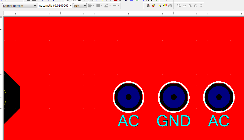
What is the meaning of the four triangles around the hole to the left? It is a layer on multilayer design. See the attached figure.
All I can say is that more, if not all, page layout systems use the "thermal optimization" to related to a plan of copper pads. The power supply looks pretty good - we use this technique with a senior system Ultiboard for decades and never had any problems with pins of caliber of several amperes power supply.
-
In utiliboard, how electrically connect my hole to the ground (it will come to a Center tap of transformer) to my plan of mass?
There may be a few things here.
1. the most common is that you can have a net 'GND' and a '0' net. 0 references usually analog gnd and "GND" usually refers to a digital pattern. Electrically they are not bound together unless specifically call you this in Multisim (Options-> properties sheet-> PCB tab-> ground option (checkbox). To annotate a forward at this stage.
2. you can't have tied together the plan that you created (what is a copper box or a Powerplane...?) with the net OK. Generally, it will be because the area of copper that it does not prompt you for a name of net before generate the plan. To check turn them on the filter selection of 'Zones of copper' and click twice on the flat surface - go to the "zone of copper" Properties tab and check the correct connection is made.
3. There are times (especially with pins SMT at VIAs), when the connection hole does not appear until you do a connectivity check (even if it is made). For TH pins should not be the case, but its pretty easy to hit the 'check' connectivity once to check (design-> check connectivity)-the style of thermal back-up now will appear if this is the case. It is a known issue and R & D work for the next update.
4. Finally check that the net (GND or '0') is related to the "GND" transformer PIN. To check, go to tools-> editor of Netlist and navigate to the 'MASS' or '0' net and check the connection is made to the correct pin code/refdes.
5. If all else fails, contact our support team and they will be able to guide you through the steps:
http://sine.NI.com/apps/UTF8/NICC.call_me
The Group has indicated if one of them solve you your problem.
Kind regards
Pat Noonan
National Instrumetns
-
Difficult to change the width of talk about thermal discharge in Ultiboard
I'm trying to change the width of talking thermal relief of various buffers on an existing Ultiboard layout done with an earlier version, and that they do not change. Can I change the "type" for x or +, etc. but not the width of the shelves. Is there some global setting prevent this? That means "use the polygon settings' when you set the type, and how will this affect the width talking thermal relief? I see nothing in the help file. I also searched help and the user manual for what happens if I select Auto for width, but I can't find any instructions on what it means.
I was able to confirm the behavior you're seeing where the width of the rays is limited by the width of the measurement of the surface of the coppe / diet plan. It is certainly not intentional and I produced it for R & D to address a defect report. I am very sorry for the inconvenience that was done to you.
There are no files attached on your post so I can't confirm your actual designs. Please let me know if the workaround solution (to adjust the width of the measure) will allow you to get the results you're looking for, despite the incorrect behavior.
Jeff
-
Ultiboard make printer laser method
Hey guys im new to this program. I got a diagram, transferred to ultiboard, autoplaced and routed automatically. I have some problems. One I want to use the method to fabercating the real jury laser printer. When I'm putting my copper layer on the top not the bottem highway. How to fix this? And also I need to print a mirrored from the actual size of the copper layer. I couldn't find that. Sorry for asking here guys but I spent like 2 hours looking in the help file. Im a student in electronics and this is my first design of the card.
Kevin
Hey Kevin,
It was the missing piece of information. Boards front has had problems and have been removed in the latest version to avoid problems such as this one. Of course, it is always possible to create them (it's just a two-face where it is not used).
For your second question, you can change the shape of the cushion directly in Ultiboard.
- Make sure that the selection filter, Activate by selecting Pads and SMD by selecting activate Pads , are turned on (I don't know if this part is THT or SMD, so this covers both cases)
- Press the Select button, then click on Edit > properties (double click also works)
- You can change the form in the dialog box that displays on the tab of Pad . If it is a part of the THT, you will need to change the shape, on each layer of the Board of Directors.
A last suggestion (dealing with nestor) is to make sure that everything is once you're done. You can do this by printing the Board with footprint of paper and making a Visual check of the part.
-
Effect on correction of the CJC to use copper instead of type thermocouple extension cables
Hello people. It is is a kind of "phenomenological" question, lumping together a bunch of real problems. Type of hope that someone had experience try this and can give me an advice.
I'm looking to make measurements of temperature relatively high speed with very fine wire of type K or N thermocouples.
I will be very many TC - about 75 in quantity and therefore will be, if it works well enough, wire the asymmetrical (I trading accuracy for amount in light of the SCB-two 68).
My complete data acquisition system is:
Computer PXI
PXI-6225
(Qty 2) SCB-68
QUESTION 1: Any recommendations in the configuration of these two NRSE or GRSE? The device, I am close to (but not electrically in contact with) is completely without merit (experience of combustion). TC fine wire is indeed very thin, and their not armoured lengths will be about 12 ". There is no significant EMF/EMI around my experience. I will experiment but just wanted to know if anyone can rule something here...
QUESTION 2:
Important points:
- I want to use type N for additional above K to my temperature range and also because that N-type are available in smaller caliber (0.003 ") and stability welded end to end.
- Unfortunately, I n ' t has a bunch of N type connectors - if I have to use/buy the N type connectors this is a significant cost (see the stop).
- My Setup has the TC in the physical location of 'groups' of 7. Given the asymmetric configuration, I have 7 anodes and 1 single "reason" for each "group" - for a set of 8 wires out of each "group".
- I need to connect on the order of 80-wire in both SCB-68. I try to minimize the number of threads that I have to deal with.
- Omega does not sell single conductor wire anode and cathode for the N-type as they do for K-type. They sell only duplex son.
- Omega is also not sell armored bundles of type N, as they do in K-type
- If I use type N TC and I use the real N type extension wire, it will have to be duplex (because of two previous points) - it's something like 80 PAIRS of wiring, with one of the sons of the cathode on most of the wires not used (because of the asymmetrical configuration).
It seems that I must consider the following compromise:
Use the TC type desired N and treat approximately 80 pairs of duplex wire extension of type N OR less desired TC type K and purchase grouped, shielded wiring to minimize the mess of wiring GOLD copper use extension (WHAT?)...
Yes! Why can't I use the copper wire extension to the fine N TC of the cable type and connect to the TC with a kind of nonmetallic connector (like screws nylon) or solder? The attraction here is that I could use the signal wire 8 drivers together, to each of my TC 'groups '. This would reduce and clean my wiring and not need to buy all type N connectors (TC would be wired, no connector involved).
It seems to me that I could simply set up the cold welding (CSF) on board the SCB-68 fixed to work on N-type. Copper wire would result of the SCB-68 the TC type N. No metal connectors would participate. Thusly, being only one junctions P/OMEGA-copper and copper/OMEGA-N to deal with the CCM. This sounds like it would be exactly the same as a N-type wiring directly into the SCB-68, except that there may be error between the temperature reading to the CJCS and the junction of alloy copper/OMEGA real. This won't be a significant error because the two locations will be very close in temperature.
If this "mistake" of temperature becomes a concern I can mount a TC that is unique to the copper/TC junction and make my own corrections (I think...)
Here is a little schematic text (without taking into account all shunt connections in the CSR circuits...):
Any circuit anode/channel: SCB-68 Terminal-> extension copper-> (direct connection via the non-metallic connector) OMEGA-P of the N type TC
Common ground circuit/channel: SCB-68 Terminal-> extension copper-> (direct connection via the non-metallic connector) OMEGA-N to the N type TC
This idea implies that the circuit board within the SCB-68 has copper conductors, such as the addition of copper extension wire would not create an additional junction.
Anyone tried this? Can someone offer me some ideas?
THANK YOU in advance!
-Dan
ddml wrote:
Henrik-
Thanks for the very useful reply. Yes, I forgot to mention that the lengths of wire extension will be the order of 1 m, then resistance extension must be low, even if common ground is used as part of an arrangement of asymmetrical circuit.
...
Here's my last logic!
- If my experience shows that the single-ended NRSE GRSE arrangement response or "match" the differential response conservative, I will choose asymmetric for more sampling points.
- Since I know the extension wire / TC to the ASE will be nearly isothermal with the CBS itself, I would like to use the extensions of copper and accept (and possibly correct?) the error based on the temperature. I would like to use threads, as this I need 7 + and 1 ground by grouping of 7 TC to my DUT (Recalling)-> http://www.newark.com/jsp/content/printCatalog.jsp?cat=c127&page=1199&display=zoom
- If during the examination of the previous point, I find that copper extensions are NOT practical and I need to use tank extensions of TC-metal all the way, then I choose a TC type K on an N-type. The reason is that there are many more options for tanks, bundled extension cable type K (N-type is apparently a sort of new and not very popular). However if copper extensions are possible, then I'll use the TC type N, motivated by their superior high temperature oxidizing atmosphere stability and the fact that I can get them in a configuration welded end to end to 0.003 "caliber!
If none of this logic seems faulty or unrealistic, I would appreciate it really more input! I don't know that it will be a lot of work!
Thank you once again,
-Dan
Dan,
I've marked the important phrase
 what you're actually doing is moving the CCM of the CBS for the TC/copper connection. Any difference in temperature will directly add to the error.
However, don't try to save the copper with your approach to 7 + 1, ask IT for another 12 m Ethernetcable guys more and go with 7 * 2 + 1 pair of reserve and make the summary at or near the CBS. IF you need a differntial measument system later, you need to rebuild all connections. (And not just add a new cable for all conical fittings, it is the twisted pair that makes the magic
Yes, same vor 1 m!) Remember that you are dealing with µV! And since you want to quick reads without filter a lot of way, do not try to save $10 to about 12 m of cable. Somehow I have the feeling that you try you anyway -
Difficulty working with the ground plane...
I am using a ground plane with '+' style contact to the parties. With a width of talking to. 010 ", contact the parties in many places is too skinny, but its just for others. This fact prevents me to extend width talks to solve the problem.
I tried to add traces of copper manually, but the plan of mass resists my efforts to redirect the traces or refusing to connect them to the plan altogether.
How can I increase plan connection of parts, without forcing on them?
Thank you very much, Tod
Hi Tod,
Him spoke with can be specified to SMT/THT pads. Normally, they are set to inherit the properties of the area related to copper, but you can change this on an individual basis.
To change the width of speaks for a special touch:
- Check that only Edit > selection filter > activate by selecting Pads and Edit > selection filter > SMD by selecting activate Pads are checked (appears depressed)
- Select the key to be changed (you can drag to select more than one at a time
- Click Edit > properties
- Select the tab of thermal discharge
- Change talked about the width of your required
-
How to remove the layers 'recovered' Ultiboard design
I designed a 4-layer Board and later, he had to change a number of prints of the parts.
Before, I annotated the new data of Multisim and lost two inner layers of the design (or so I thought).
I rebuilt the two inner layers from scratch, registered and closed design.
Open the file the next day, I discovered two extra layers "recovered." My drawing has now 6 layers.
I tried to remove the layers recovered, but I can't do it without losing information of drilling as well.
Is there a safe way to extract recovered segments of the design without losing the drill news?
Thank you very much, Tod
Hi Tod,
"Recovered layers" is created on opening a file if Ultiboard find objects that refer to layers that do not exist in the Council. As a general rule, it should be safe to remove these layers in the dialog box properties of PCBS, because these objects are usually copper coins. First of all, you need to remove all the objects of these layers. An easy way to do it is:
- Right-click and hold, dragging the mouse over your design (similar to the way you would normally select with the left button of the mouse)
- Release the mouse button, and displays a context menu
- Click Select objects on layers specified...
- Select one of the layers 'recovered '. Click OK.
- Edit > delete
(I feel like I could be missing here and if so, let me know).
Maybe you are looking for
-
I hate the new updates! I love type horizontally when I text and now I cannot since this morning when I did the update. When I turn the screen all these pre's words come as 'Hello' help! I want to go back before update!
-
Problems with speed of Pre adjustment knobs
I have a problem with setting new calls abbreviated after the last update1.3.5.1. Since the last update I can't put a new speed dials. I go to the contacts app, select the contact that I want to put a speed dial. After you select this contact I tap t
-
To the frequent insistence of Apple, I installed El Capitan. We will leave aside the quality of the software, but foolishly, I kept it El Cap for a few weeks. Finally, I went to the Apple store, the genius bar. Long story short, I can't access a p
-
Impossible to re - download workout
I tried to put in place a multisport training (10 minute warm-up run, interval repeats, 10 minute cool down) and he ran today. I must have misconfigured training because the instrument does not start automatically run interval activity after the warm