copper box
I'm editing an existing card that has copper complex areas (aircraft on ground) at the top and bottom.
When I try to move or to place a component the program virtually stops, allowing only spasmodic component movement choppy while it redraws the copper areas.
How can I disable the refreshment of copper areas without deleting them (I do this in other programs of PCB layout, but I can't find a way in Ultiboard)?
PRH
Here are a few possible suggestions:
(a) first of all I suggest to change the zone type to outline only (instead of solid). Polygon properties.
(B) or you can choose to temporary turn off verification in real time of the DRC. Ultiboard setting.
(C) or you can disable the invalidation. Polygon properties.
Change the settings back when finished.
Kind regards
N Pat
Tags: NI Software
Similar Questions
-
I want to create a completely blank copper on a plane in copper.
I want to create a completely blank copper on a plane in copper.
/ When I create a copper box and then select fill 'none' there is always a small ring of copper around the perimeter which I can't delete regardless of what settings I use.
Hello
There are two ways to do:
(1) after having placed your aircraft in copper, put you on the layer 'keepin allowed/forbidden zone '.
go it to 'Place' "Keepin-forbidden zone" and draw the shape you want.
Then the area will be cut off from your plane.
You can get errors in DRC with parts and titles in another layer.
This can be avoided, but takes a lot of settings... so I never have that
(2) instead of having a plan in copper, use copper areas to build your airplane.
You might need to put two or more overlapping region,
So just don't put any copper where you don't want everything.
This solution is somewhat more difficult, but you get errors of DRC on other layers/parts
Success!
-
connecting the trace copper, copper a region away from track
I set the nets to be the same, I'm not crossing layers, but when I try to connect a trace in the copper region that I created, the copper area shrinks from the trace. 010 "(constante d'espacement)." Is there a way to avoid this? (Ultiboard 10.1.1 / win XP). Thank you very much
Right-click on the copper box, and then select Properties. In copper network properties dialog box select copper area tab select connected to the net , and select the Web you want in the list.
-
Urgent! reading problems in area v5 UB DDF files, copper
Hello
I have a very strange problem with Ultiboard.
When you read an old DDF (v5) file, it is opened and converted to ewprj...
I have no schema file (paper only version) and no netlist...
Traces of not obsolete should be changed to the more recent...
so far no problem, I inserted everything manually...
It is a Council of four layers with several areas of copper on the inner layers.
When you export data, gerber RS274X, then the weardest things happen...
Of via which must be tied to GND accompany the + 5V
I have found that while old and new checken gerberas with GCprvue...
So I checked the design:
the parameters for any copper region are correct! for example: area of copper on the inner layers are defined as follows
Inner1: Layer of GND, enable invalidation, connected to the net GND, without thermal reliefs for the via of
Inner2: + 5V layer, enable invalidation, connected to the net + 5V, not thermal of the reliefs for the through the
but during the audit, the layer of EARTH is not connected to the MASS of via, but the 5V is layer...
! There is a void in the SOIL layer while it shouldn't and the 5V layer is connected,
And the strangest thing: when you run a check of the DRC, you get all the defective connections!
When you look at the original file, after that I just opened it, then everything is ok...
Maybe this will give you a hint more:
sometimes without apparent reason, there is no more fill style in a copper box, he disappeared.
everything you see is the outline of it...
As soon as you start working on the original design, things go wrong...
Can anyone of OR extract it? This happens quite often in the design-updates to update...
I use UB version 10.0.343
the attachment are screnshots with GND (green layer) and parameters of 5V (blue layer)...
Johan
Hi, no, through the should be attributed to the net (trace) they are placed, never found any problem with this... But the good news: I finally found the problem, after many hours of research... I have already mentioned that he had more no styme filling in an area of copper number '... Well that's how I finally found the problem... On one side of the Commission, that I had to replace a 16 pin IDPS by a through hole connector 4 pole. Inside 5V layer, the original designer exceeds all the necessary tracks connect connections 5V together... One of these titles (which you don't see when the fill style is full) affected a brooch of the new via the connector hole. Thus connected to 5V, and this pin should be rectified in the updated design... which causes a short circuit... a little of these layers apparently caused through the 5V to be connected to GND on the complete picture... Which makes it very difficult to find the problem... Only after I've changed the 'no' fill fill style, I could find the connection... Can NEITHER find a way to get this problem easier? When to see the faults of DRC all around the plateau, it is difficult to see that we actually really causes the error best regards Johan
-
In utiliboard, how electrically connect my hole to the ground (it will come to a Center tap of transformer) to my plan of mass?
There may be a few things here.
1. the most common is that you can have a net 'GND' and a '0' net. 0 references usually analog gnd and "GND" usually refers to a digital pattern. Electrically they are not bound together unless specifically call you this in Multisim (Options-> properties sheet-> PCB tab-> ground option (checkbox). To annotate a forward at this stage.
2. you can't have tied together the plan that you created (what is a copper box or a Powerplane...?) with the net OK. Generally, it will be because the area of copper that it does not prompt you for a name of net before generate the plan. To check turn them on the filter selection of 'Zones of copper' and click twice on the flat surface - go to the "zone of copper" Properties tab and check the correct connection is made.
3. There are times (especially with pins SMT at VIAs), when the connection hole does not appear until you do a connectivity check (even if it is made). For TH pins should not be the case, but its pretty easy to hit the 'check' connectivity once to check (design-> check connectivity)-the style of thermal back-up now will appear if this is the case. It is a known issue and R & D work for the next update.
4. Finally check that the net (GND or '0') is related to the "GND" transformer PIN. To check, go to tools-> editor of Netlist and navigate to the 'MASS' or '0' net and check the connection is made to the correct pin code/refdes.
5. If all else fails, contact our support team and they will be able to guide you through the steps:
http://sine.NI.com/apps/UTF8/NICC.call_me
The Group has indicated if one of them solve you your problem.
Kind regards
Pat Noonan
National Instrumetns
-
Internal matter on the placement of Vias on board four layers with TWO planes of Earth
My design is a four-layer Board. Surface upper and lower layers are for routing of traces and power. Two interior floor plans (the preceding the other separated by an insulating layer) are for all ground connections. Customer specifies that all ground connections to make for TWO inner floor plans. When I try to place a via that will connect a trace on the outer surface to the ground, I'm not allowed to connect to more than one internal plan.
I need to place vias completely through the Board of Directors and connect a trace in inner outer surface for TWO floor plans... Is it possible or assignment that will allow me to do?
Ultiboard V10.0.144 running.
Thank you
Solved my problem. Do inner Layer 2 the active layer, turn off all other layers. Internal stressed Layer 2, r/c on the Properties tab copper box, click connected to the Net, drop-down list, choose DGND, apply, OK. Now place a via. R/c, choose Properties, tab, click on assume net, drop-down list, choose DGND, apply, OK. via moment connects to the inner layer 1 so much inner Layer 2, b/c, the two are now associated with the net DGND.
Beautiful - thank you...
-
Hello
I have my laptop for several years now, but recently it has become very hot, and the fan continues blowing loudly. As the guarantee of the laptop disappeared for several years now, I decided to open the case to clean the fan and apply new thermal paste. However, when you remove the fan I noticed several black thermal pads on some of them, for what I guess is, GPU chipsets. The pads were very dusty and cracked. I cleaned the fan and am now trying to figure out what I can use as a substitute for black thermal pads. I guess than regular thermal compound from the CPU is sufficient for GPU chipsets.
Heat sink code is:
HP 534684-001 SPARE PART
Do you have any idea what I can use?
Kind regards
Soden
The black keys which you reffer are carpets made from Silicon heat transfer. I looked at your radiator, and the picture shows a copper box that is for the cpu. I would recommend artic silver or a similar compound high range. Silicon pads can be had online (example):
http://stores.eBay.com/best-computerparts/soft-thermal-pads-/_i.html?_fsub=2445042013
The color can mean either thickness or rate of heat transfer. This is the most difficult part that most retailers ebay do not list the rates of HT, but nothing in the 1.5 - 2.0W range will be just fine. The most important is the thickness. You don't want to make too thin as so it will not make good contact. Not thick or it will prevent other areas of the radiator to make good contact.
I'm trying to find the best rate HT. If you have to you can stack the pads, as Silicon will give a little and it will not affect heat transfer. Beware of the shims. Not done properly, they can put undo stress on the Inserter and subclassing leading to failure to chip.
-
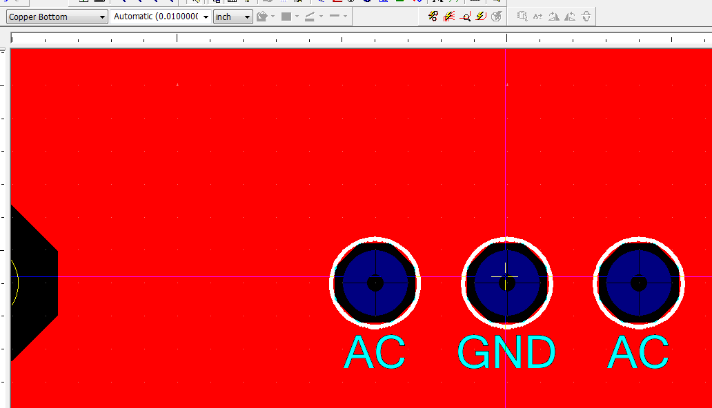
Hi all
I use Ultiboard 12.0 and I need to create a box full of model copper.
I already found some docs on the internet claiming that it was sufficient to change the style of 'fill' of an object in copper. While he was trying, I see this option but when I change the style of pattern that makes no change, the area is always drawn as a strong region. It may be only a display bug, but when I try to print the copper layer it prints a solid.
Any help would be greatly appreciated.
Kind regards
Aya
Aya,
Try this:
Right click on the area of copper in which you want a hatch.
then select the type of door you want (copper area tab)
go to the 'general' tab, and then change the width value...
If it is too small or too big, the hatch appears as an area full of copper
success!
-
Diagnosis copper wire test on SG200-26 Gigabit Switch - what is the "open cable" telling me?
I have installed a Switch Cisco's Gigabit SG200-26 to the installation of the client. They have a severe latency on their network, so I was hoping the switches capacity could help me track down the problem with the statement. There are 7 computers in white box on the switch. Six computers have been sold at the same time and have the same motherboard. A computer seventh was sold a few years later, and has a different motherboard. All computers have the NETWORK card on the motherboard. All seven computers come with ' Open Cable - cable is connected on one side "when the analysis of the copper is run under the Diagnostics tab. Each test has an inclination of NS 8 pairs at least three reports four sons. A router, server Dell, Cisco wireless router, used only as a point of access, an old computer (about 10 years) and a small Netgear switch good show all in the analysis of copper. Each node is except the switch Netgear gigabit speed and the old computer. None of the ports that are attached to the computers display errors.
Thinking that maybe the wiring of the installation is all bad, I took a computer to the switch and connected a connecting cable of known network and in a good 5' from the computer to the SG200-26 Gigabit Cisco Switch and then I did a test of copper. The results were the same - "Open Cable - cable is connected on one side.
I am completely confused by all this. First of all, what exactly does "Open Cable - cable is connected on one side? These computers can access the Internet and the server and sometimes seem to have hours of access to resources, so I know both ends of the cable are connected. And what is the inclination was trying to tell me? Is it possible that all 7 computers, which are Windows 7 32-bit and a couple of 64-bit operating systems have a driver problem?
Help here would be most appreciated.
Hi txlmbardi_2,
This really should not conduct so please open ticket with Cisco Small Business Support team to deepen this review:
http://www.Cisco.com/c/en/us/support/Web/TSD-Cisco-small-business-suppor...
Kind regards
Aleksandra
-
Unable to select the file in the dialog box in the Sierra
I'm unable to select an image file in the "save for Web" in the finder window "save under" in Photoshop CC running on the Sierra.
There are times where I need to save a new image using a similar name by selecting the existing file, which matches the name in the dialog box "save under".
The use of Photoshop CC in Sierra I am unable to do so due to the inability to select the existing files in the Save-as the finder window.
I thought at first that was Adobe, but later, I noticed that I can not save for web browsers and other programs. I installed the beta updates on Sierra, but also which did not set. I hope be fixed so I can move on to Sierra. It was not such a problem in previous versions.
Unfortunately, your discovery is correct. I just met for the first time. I was shocked, but apparently it will work in list view. View miniature not a reason any.
-
box from Apple tv to a computer screen (screen only) can I do this?
mirror of my ipad to a PC screen (not connected to a computer)
is it possible via apple tv
I connected HDMI from apple tv to a screen of PC DP.
then try my ipad screen to the screen of the PC via applies mirror box
reason is my security cameras use "OHS" and it works that vi an app (not on PC)
So I want to project of the ipad to a larger screen in my living room
is this possible?
or does anyone know of an app that I can use on PC that is the same as MEye?
You should be able to use an hdmi, dvi, and port (if it supports hdcp) directly, as they were TV
but the port hdmi or display in a computer is out only, some TV tuner boxes can support hdmi in but do not know if they could manage the hdcp encryption
-
Box of complete junk mail on iphone but not mac
My filters junk mail very well on my iphone and ipad; but I have a practically empty spam folder on my iMac which paradoxically is not good; because I lack important emails sometimes end up there.
I shouldn't get the same box of junk mail on my mac and on my iphone? Why the my balls mac is empty? Missing important emails. Is it related to the e-mail servers imap vs. pop?
Thank you
It could be, if you use a POP system only the first client to get unwanted has it in her junk folder, if IMAP, all will be.
-
Save file dialog box can't name.
Hello!
I've updated 5 macs in my household to Mac OS Sierra. Mac Mini, two retina Macbook and iMac 5K. None of them are able to pick up existing file name when you try to save a file. I used to be able to click on a file on my disk and it entered the name of the file in the Save dialog box, but the entry in the right field remains empty and I have to write the name of the file manually. Really frustrating when just in collaboration with revisions and you want to change the last number in the file name.
Anyone else experienced this and maybe have a fix?
Thanks in advance.
Tom
Your message has caused me to try this using two different applications (Apple Pages) and overview of the MacOS. In both cases, when I open an existing file, his name came up in the center of the window. Also, when I did a "Save" or "Save...". "this file name was introduced as the default name. in other words, a backup would just replace the existing file.
The behavior you describe is clearly based on what application you are using. You did not specify which application could be.
-
Hello my fellow partners Mac!
This seems to be a common problem, whenever we have a new version of Mac OS, but I can't, from my POV, find the right solution.
Every two hours or when waking from sleep, a dialog box appears telling me to install a Java Development Kit. As I said, this has happened many times before when you Google, but I can't find someone who offers you a solution where you don't need to install the JDK. It seems that the only solution is to succumb to the demand of the dialog box.
In my case (and this may vary, I'm not sure), it is the launchd process that requires it. But I can't go further than in my knowledge of the OS. I tried to delete all the files about kinds of Java and have looked everywhere for stuff that could trigger this, I deleted LauchDeamons, LaunchAgents, all related to Java I could remove in / System / * and (~)/Library/* etcetera, etcetera, but this dialog box keeps popping up, so something ask and I cannot understand what it is.)

What I need, is not install Java. I don't like, and I think that it is an old and dangerous technology. I want to just get rid of it all once and for all (and if all goes well, without having to reinstall everything form scratch).
Anyone can shed some light on this? It's the system itself that think I need this, or is there a way I can dig deeper to understand what triggers it?
See you soon,.
Massimo
What I need, is not install Java. I don't like, and I think that it is an old and dangerous technology. I want to just get rid of it all once and for all (and if all goes well, without having to reinstall everything form scratch).
Anyone can shed some light on this? It's the system itself that think I need this, or is there a way I can dig deeper to understand what triggers it?
The operating system does not use Java in some way. You have installed software that only requires Java, but it must also be Java 6 legacy published by Apple (and abandoned) years.
If you don't want to install Java, you must determine what software you have installed which requires Java and remove it. From what I've seen here, it's generally Adobe software that appears to have been poorly coded to only use the Apple of Java 6.
-
iPhone made his but without alert box new email
Hi all!
This problem lasts for at least a month now, so I figure it's high time to ask about it. Several weeks back my iPhone 4 has stopped to give me a new email alerts. I have all my accounts the value 'Badges, sounds and alerts. I get the sound / vibrate when I get a new email but I DO NOT get an alert box. It was always nice to get a glimpse of emails and I want to come back.
Of course, I receive pushed emails I get sound. Anyone has any ideas on where to go from here? The problem persists after a reboot.
Thank you!
Did you also set notifications to display on the lock screen?

Maybe you are looking for
-
Watch locked after resale - purgatory
Hello I just sold a Apple Watch on eBay. I have reset before sending it. The buyer cannot pair because it is related to my iCloud account. I wasn't aware that aveillez was locked in this way. My watch does not appear in iCloud > parameters as one of
-
How can I fix my screen to allow an older game to work?
-
How can I install AotoCad 2007 in Windows Vista Home Premium please?
I just installed AutoCad 2007 on my laptop running on Windows Vista Edition Home Premium, only to discover that they are not compatible with each other. Is there a solution to the problem please? Thanks in advance. Karl
-
Issue of scanning HP Officejet 7612
I can't get my HP Officejet 7612 to analyze. I use Windows 8.1. I ran the HP printer Installation Wizard. Test print was OK. Analysis of test was inadmissible. I ran doctor printing & scanning HP, but it keeps stuck on Windows (WA) Scan. Is si
-
He said that it is too big to send, to reduce the size by removing one or more attachments. The size is wmv.37.0mb I didn't shorten what is my grandchildren. If I had to, how would shorten this video for e-mail? Thank you What