FPGA - series C of NI 9215
Hello
I am a new mechanical engineer on FPGA and LabVIEW Real-time. I was trying to connect a sensor accelerometer for the NI 9215 Module of the 'C' series in the controller chassis 9024 cRIO but lives a hard time to find the right connections, especially with the 'GROUND '. I would appreciate a lot any effort giving me more insight on the problem that I am known and help me acquire a voltage signal. I went through various white papers, but none of them explained in detail.
Hi KarthikSrinva,
What you have described might work, but don't forget that the 9215 has a maximum range of +/-10V of its own reference to the ground (COM).
Because the battery is a floating (unreferenced) voltage source, you'll want to fill them HAVE - COM (common ground) terminals and to ensure that you have a common reference and the differential signal is not float out of reach of data acquisition. What is described in Chapter 3 of the guide to wiring field and noise considerations I think you were talking about earlier:
Wiring and considerations of noise for analog signals
http://www.NI.com/white-paper/3344/en/#toc3
Kind regards
Tags: NI Software
Similar Questions
-
FPGA. What tool xilinx for Crio-9022 & 9030
Hello. I will be compiling the programs of fpga on the Crio-9022 and 9030. You need Xilinx different compilers to do the task?
With the help of LV ver14
CRIO-9022 requires xilinxs 14.7 tool?
CRIO 9030 requires the xilinx tools vivado 2013.4?
Thank you
Yes, it's because of the different FPGA series located on the backplane of the 9022 and 9030 cRIOs. You can see this KB and this KBto see below why.
-
NEITHER USB-8452 - reach the maximum write SPI speed
Hello
I have a USB-8452 with the latest version of the software installed (2.1.2). The host computer is a Core i7. I am trying to achieve the maximum SPI write speed with the camera possible. I tried the basic block read/write SPI, SPI Scripting blocks and SPINNAKER streaming, but the first two have large delays between CS falling and the data being written (with so that delays in loop), and the last seems to be useful only for read operations.
Can someone tell me if there is a way of a) reduce the time of installation for basic SPI / SPI Scripting or b) writing different values in a single stream of SPI? Thanks in advance for any help on this issue, even if it's just confirmation that yes they is hard limits that cannot be overcome with the LabVIEW 8452 interface at this time.
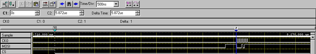
Here's the best I can do right now, as shown in my logic analyzer. Change of the SPI clock speed does not affect installation time and delays that are primary and secondary bottlenecks:
SPI read/write database-
Program: Basic Configuration followed by read/write of SPI block itself in a while loop
Main bottleneck: ~ 450 delay us into iterations of the loop (see Figure 2)
Secondary bottleneck: ~ 6 us delay between falling edge of CS and the first synchronization signal (see Figure 1)
Capture 1 - delay highlighting between CS falling and first SCLK pulse
2 delay highlighting between all iterations of the loop of capture
Scripts of SPI-
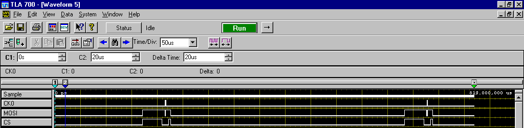
Program: Followed two Script blocks Basic Configuration run in a while loop (to check the two block to block and delay loop iteration)Main bottleneck: ~ 450 delay us into iterations of the loop (see Figure 3, space between the second and third images captured)
Secondary bottleneck: ~ 250 us delay between blocks of Script run consecutive (see Figure 3, space between the first and second captured images)
Capture 3 - highlighting delays consecutive run the Script and delays between while the loop iteration
SPI in Streaming- It's the closest to achieve a fast writing speed, but unfortunately, it seems to be only useful for read operations (e.g., ADC), do not write.
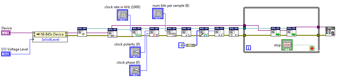
Program: Configuration of the base stream followed by start of the flow block
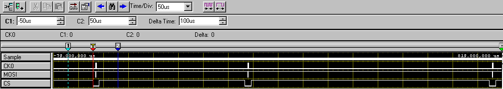
Main bottleneck: impossible to write something else than the data value unique property "wave 1-> MOSI data." I can write a byte array to this property, but it will simply put all these bytes in an image and repeat this framework (see Figure 4) rather than go through each value.
4 - two bytes sent repeatedly using SPI capture stream. Delay of CS is finally good, but no possibility to change the MOSI image to image data.
Hi JBender1,
This show looks like what we would expect for a 8452.
If you need higher performance, I encourage you to watch using a card R or FlexRIO FPGA series for your implementation.
-
Synchronization between PCI - 6251 / PCI - 7811R
Hello
I need to synchronize two card PCI, PCI - 6251 / PCI - 7811R. This is my first time with a huge app, and I don't know where I should start.
PCI - 6251 I connected SCXI - 1001, (in chassis: SCXI-1161,-1326,-1327,-1125,-1324) and I'll use it for measurements. Through the PCI - 7811R I want to communicate using the JTAG Protocol, SPI and meaby measure PWM signals. I'm not sure that anything is possible.
Please help me or give me some tips where I can find some examples.
Kind regards
__behemot_
Hi __behemot_,
First synchronization between these two modules can be done thanks to the RTSI, the easiest way bus. The two modules must RTSI connector, so no problem should be there. You can find useful information on the RTSI bus on the following link:
http://zone.NI.com/DevZone/CDA/tut/p/ID/4322
Also search NI example Finder on RTSI, you will find beautiful examples.
Concerning the programming of FPGA section, the following links are of course useful when it comes to digital Communication Interfaces and PWM on FPGA:
http://zone.NI.com/DevZone/CDA/tut/p/ID/5385
http://zone.NI.com/DevZone/CDA/EPD/p/ID/4725
Please also check the NOR example Finder (easier to find in LabVIEW is the Help menu): in search for a selected tab Toolkits and Modules--> FPGA--> series a. here you can find a lot of examples that may be useful to start.
Let us know if you need anything else!
Best regards
David Varga
Technical sales engineer
NIH
-
LabVIEW FPGA SPI accident - SPI OR IP address for example - R series OR
Hello
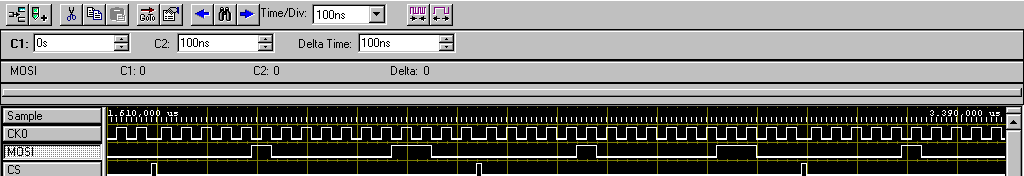
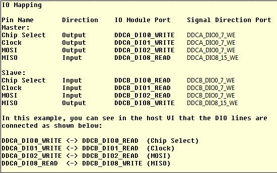
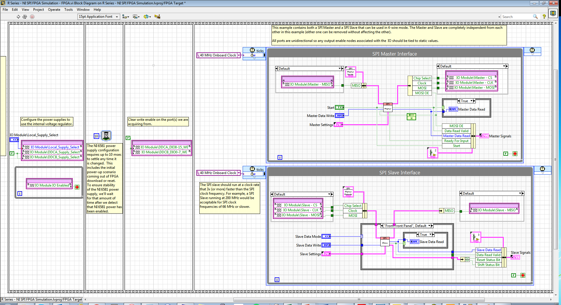
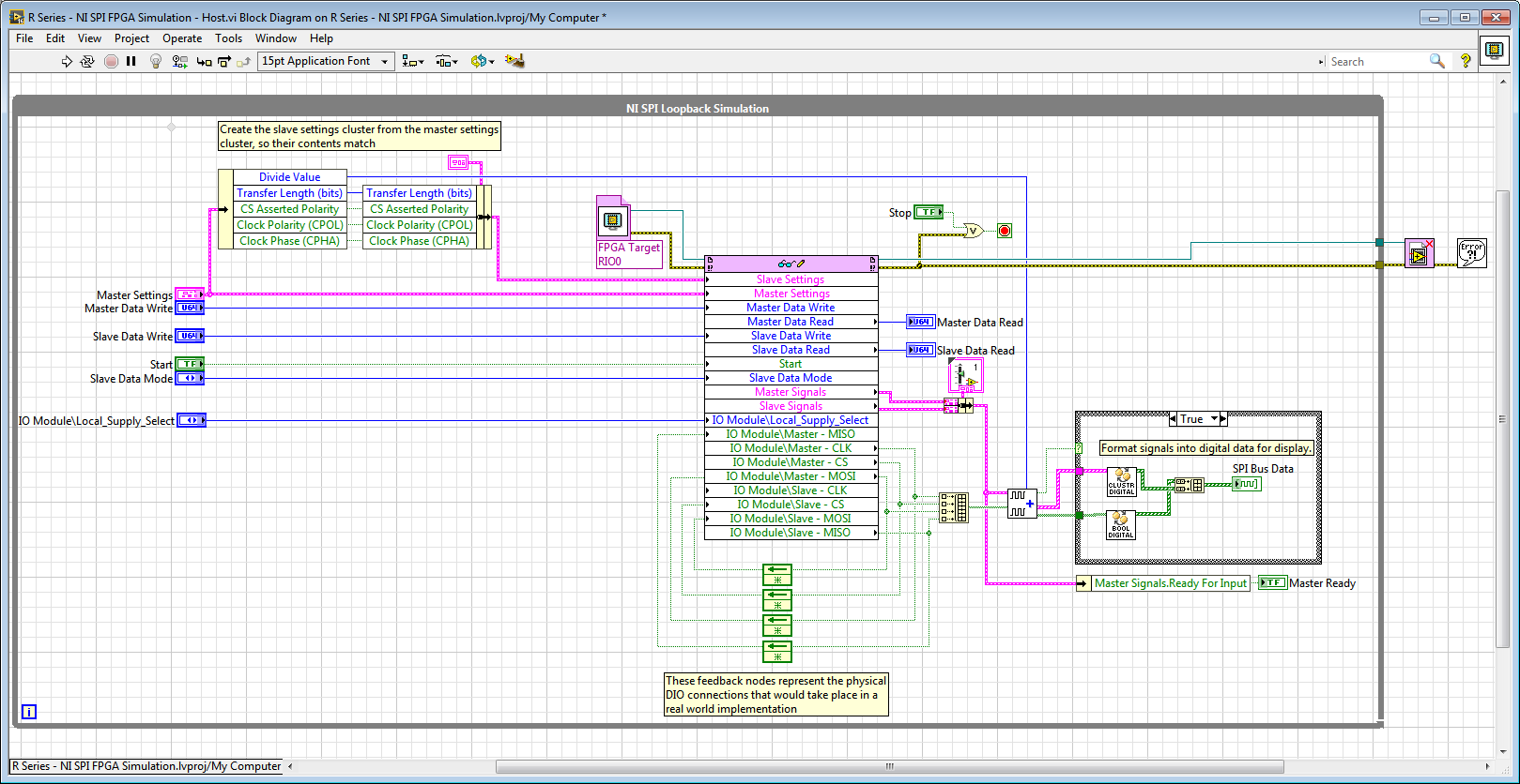
I am trying to run the series R - sample project NI SPI FPGA Simulation.lvproj that comes with the SPI IP OR on a real FlexRIO FPGA SMU-7976R target with an attached digital adaptation NI 6581 B Module. The example is for a PCIe-7841R but I wore during my target FPGA, follow these steps and made additional changes to try to make it work with my set-up. I learned that FlexRIO FAMs CLIPs do not work with nodes in office had so I know I can't simulate the project originally planned so I will try to use FPGA to e/s node host side (open FPGA vi reference) to implement the actual hardware.
My first question concerns my configuration of the adapter module e/s and selection. I added the IO Module (NI 6581 B: NI 6581 B channel) for my project and selected the channels as shown in the table below. I have a real physical hardware connection as described below using two NI SHC68-C68-D4 cables and a break-out Board.
I changed the names as well:
I selected these DIO channels because I wanted the DDCA connector to be the master and the DDCB connector to be the slave. In addition, in this CLIP every eight channels of i/o has a write enable signal. I have not used the Port configuration because I needed 4 available DIO channels and I saw DIO0-3. Is my logic of selection of channel vs correct Port here?
Following the same strategy that examples FlexRIO/NI6581B, I changed the FPGA.vi to include initialization outside of timed loops:
And in the Host.vi I have a node reference FPGA and wired loops of feedback accordingly:
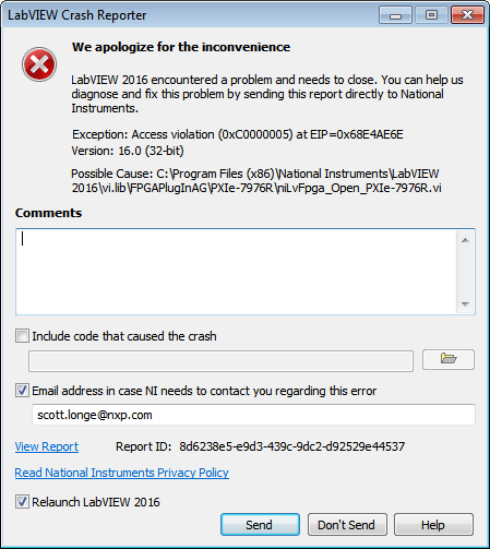
When I compile the FPGA and try to run Host.vi LabVIEW inevitably crashes with Crash Reporter below and must restart:
Does anyone know what I'm doing wrong here? My guess is that it has something to do with the CLIP/IOModule. Any help is appreciated.
Thank you
Scott
Hi Scott,.
I suspect that the problem might be related to the fact that your node open FPGA VI reference is in the while loop and trying to open a new FPGA reference at each iteration.
If you move outside of the while loop, it does not solve the crash?On channel vs port question, your logic seems reasonable to me, but I recommend to try it since this feature could depend on device.
-
Photon counting using the FPGA of the series R. problem generation TTL signals
Greetings,
I try to use the R series FPGA to read and count the pulses TTL of a discriminator (count of photons of the Hamamatsu C9744 unit) connected to a PMT (Hamamatsu-H7422P-40). The release of PMT looks fine (signal.png H7422P-40) but the discriminator wasn't able to generate corresponding TTL 5V pulse. There was some scattered and random spikes, but nothing significant. Instead, the only stable the PMT signal is a single + 5V pulse no matter how, I adjusted the PMT (C9744 output.png) control voltage. The PMT and the discriminator is connected by an ordinary BNC cable 50 ohms.
I am really confused because it was supposed to be a really simple installation. Anyone have a similar question or have similar Instrumentation (but no problem) configuration? Comments/suggestions are greatly appreciated.
Thank you very much in advance!
Hi Kelli,
Thanks for your help. Sorry it took so long to get back to you.
I actually found the question. The discrimination of the Hamamatsu unit level is set too high that all signals got filtered. After adjustment of the threshold of manuallyt, I was able to get the camera TTL pulses. And 7842R worked correctly for count impulses. Everything works fine now. Thanks again for the input.
-
The FPGA IO corresponds to which C-series e/s?
I have a PXI-7813R with connectors 0 and 3 connected to a chassis with modules of series C in them (9474, 9205, 9206 and 9423). I want to know that I/O corresponds to what e/s on these chassis.
As far as I know my FPGA project (which was written not by me) are the channels of each module of the series C are used, but I don't know what DIO channels they correspond with on the FPGA. For example, I can use the 9205 channels 0-31, but that channels 68 connector 0 of FPGAS which corresponds to?
Does anyone know how to tell you this? Thanks in advance.
joedowdle wrote
I want to know that I/O corresponds to what e/s on these chassis.
Why do you ask that? When you use Connector0 to the expansion chassis, the Connector0 IOs are more available in the project, on the contrary, the expansion module chassis and can be configured as explaind here. Also take a look at this thread.
Christian
-
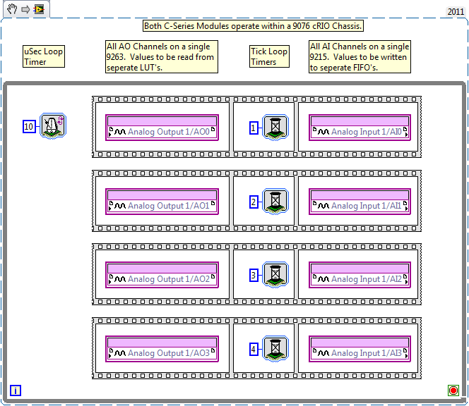
I can here sample 9215 channels separately sometimes differ by a few FPGA ticks?
Howdy-
The image below is a raw illustration of my question. I would like to individually explain the delay between excitation and response of 4 separate systems, each connected to a single channel of a 9263 (excitation) and a 9215 (response). The minimum time of update on both modules is approximately 10 uSec, so I think it would work if I just wanted to read all channels to HAVE at the same time. However, I did not yet understand internals of the 9215 that enough to know if I can taste the individual channels separated sometimes by a few ticks to FPGAS.
Thank you all, and have a great day.
Hi, BCRO,.
With the 9215, all separate channels separated from a/d converters, but still work in the same clock 100 kHz (10usec) that the module is limited to this sampling frequency.
So, in your case (thanks for the picture, by the way - it is always useful!), what will happen is that all four of these input channels of the 9215 will take place on the next loop cycle instead of staggered in one iteration of the loop.
For example, if you were to use a loop rate (25 kHz) 40usec, you can compensate for these delays at intervals of 10usec and that this configuration works, but not as quickly as you want.
I hope that this explanation makes sense, but the short answer is that we will not be able to do so during the execution of the loop in the time of minimum cycle.
-
How to choose the maximum number of items for DMA FIFO to the R series FPGA
Greetings!
I'm working on a project with card PCIe-7842R-R series FPGA of NOR. I use to achieve the fast data transfer target-to-host DMA FIFO. And to minimize overhead costs, I would make the size of the FIFO as large as possible. According to the manual, 7842R a 1728 KB (216KO) integrated block of RAM, 108 000 I16 FIFOs items available in theory (1 728 000 / 16). However the FPGA had compilation error when I asked this amount of items. I checked the manual and searched online but could not find the reason. Can someone please explain? And in general, what is the maximum size of the FIFO given the size of the block of RAM?
Thank you!
Hey iron_curtain,
You are right that the movement of large blocks of data can lead to a more efficient use of the bus, but it certainly isn't the most important factor here. Assuming of course that the FIFO on the FPGA is large enough to avoid overflowing, I expect the dominant factor to the size of reading on the host. In general, larger and reads as follows on the host drive to improve throughput, up to the speed of the bus. This is because as FIFO. Read is a relatively expensive operation software, so it is advantageous to fewer calls for the same amount of data.
Note that your call to the FIFO. Read the largest host buffer should be. Depending on your application, you may be several times larger than the size of reading. You can set the size of the buffer with the FIFO. Configure the node.
http://zone.NI.com/reference/en-XX/help/371599H-01/lvfpgaconcepts/fpga_dma_how_it_works/ explains the different buffers involved. It is important to note that the DMA engine moves data asynchronously read/write on the host nodes and FPGAs.
Let me know if you have any questions about all of this.
Sebastian
-
How to generate the clock 8,192 MHz on the labview FPGA 7854R series card?
Hello
I use the NI PXI-7854R series card that has 5 FPGA from Xilinx Vertex on him. I'm drifting clockwork 8,192 MHz to 40 MHz on board the FPGA clock. But he ended up giving me a single clock 8 MHz. is it possible to access the PLL located on FPGA Xilinx?
Concerning
If you are familiar with VHDL you can make your own "component-level IP' (aka CLIP) with a PLL Xilinx inside. There are topics for help and examples of how to define a CLIP. Here's one that shows how instantiate a DCM (similar to a PLL) in a CLIP:
http://zone.NI.com/reference/en-XX/help/371599F-01/lvfpgahelp/fpga_clip_clock_ex_code/
-
Available for PXI RT Systems FPGA scan Mode uses the R-series cards? Or you can use the Mode of the FPGA Interface to access the FPGA?
Thank you
Craig
Scan mode interface cannot be used with the r series devices as far as I know, so you want to use the read/write and DMA FIFO nodes to communicate with the FPGA.
-
How to use the modules of the series and two different bitrates in FPGA mode on cRIO 9075
Hello
I have a project with modules namely NI 9227 (module 1) and NI 9234 (2 Modules)
The project is running and I use the file writing PDM and found that two channels is in the TDMS file while I download the file using FTP the cRIO.
1 - my quesition is the addition of a second rate in the FPGA?
2 - Why is it TDMS connect 6 channels and 4 channels?
Thank you
Attached to the project with two screws
Hello Ihab,
Sorry for the late response here; just saw this message! If you want to keep synchronized modules then definitely stick with the master configuration and slave for your two modules. Note also that you can taste a little faster with the NI 9234 as your master module (since its time base main internal is 13,1072 MHz instead of the time base of the 9227 12.8 MHz).
Also, see the tips and information in our troubleshooting guide for the synchronization of the series C with LabVIEW FPGA modules:
http://zone.NI.com/reference/en-XX/help/373197D-01/target6devicehelp/sync_acq_multiple_modules/
I hope this helps!
-
Using the C-series SCTL DIO module with slower than the top level [FPGA] clock
Hey all,.
I'm running online research on a problem that I have a lot of success.
I have a chassis with integrated FPGA, top-level 9030 clock 40 MHz. I have a NOR-9401 DIO C Series module plugged and the value that will be managed by the FPGA target. I need to count some linear encoders to exactly 10 MHz, no more, no less. They are periods and gives a result of such kind that if I oversample or underestimate, I get garbage.
If I create a SCTL and assign a source of synchronization derived from 10 MHz, I get an error code generation who:
"Node read e/s for DIO3 FPGA is used in a clock domain that it does not support. Areas of clock supported include: the clock of higher and clocks that have a rate that is a multiple of 40 MHz, for example 40 MHz, 80 MHz, 120 MHz and so on. »
I tried several ways to work around this problem; First I tried just using a while loop with a loop set to 4 is ticking timer, but it then takes 9 clock cycles to perform the count for a reason any (although this code may compile in the SCTL without any problem). I then tried to use the SCTL with a constant of 'true' AS a hack for a 'timed sequence' framework-related, and that certainly has not worked.
Are there any strategies or techniques, or settings somewhere to work around this limitation on the AID I need to taste exactly 10 MHz? I'd like to do this quickly in the software and get this rolling as soon as POSSIBLE.
An image of the relevant section of the code is attached, I'm happy to provide you more things on request.
Thank you very much!
Maia Bageant
Thanks for the reply! The problem ended up being a hardware problem based on how coders were connected. Now that I've fixed it, they're perfectly happy are oversampled.
I guess my question is always legitimate to other applications, but not necessary for encoders a.
-
PCIe-7842R (series R FPGA) digital output does not work properly
Greetings,
I'm having some problem show TTL the correct voltage with my PCIe-7842R FPGA board.
The block diagram of my code FPGA LV Moose appears in "analog - digital .png '. The idea was to convert an analog input (decimal value) to a binary code and 16-bit output by 16 DIO ports. I use the connection block SCB-68 has as the terminal and trendy on the FPGA 1 connector RDIO with SHC68-68-RDIO shielded cable.
The compiled code ok. But during the test, I noticed that some ports has no output TTL levels correctly. For example, for input 1000 decimal, I would expect binary code 0000001111101000. However, some ports (DIO #6, #7, #9, etc.), which are supposed to ~3.3V (1 digital) high TTL output, output actually 0.8V. I have attached the result measured in 'exit digital test.png '.
To ensure that the question was not because of the code of the LV, I did some more tests on DIO #6 with a simple example (simple digital output.png). The output was ~ 1V this time at the digital 1.
It's really confusing because of the digital Edition is supposed to be simple. I used the same FPGA card for controlling roller shutters with TTL signals before and it worked fine.
Does anyone have similar problems? Any suggestions are greatly appreciated.
iron_curtain wrote:
DIOs are connected to a controller digital galvo Cambridge Tech. But I measured the voltage at the terminals of the connector block.
If you unplug the controller galvo DIOs, do they look good (have the right voltages). Do you know how many of these entries to the need for controller? I think you hit the limit the total current available for EID within the Council.
-
FPGA error: failed to create the C Series module
I use sbRIO 9631 with LabVIEW 2012, as well as the FPGA 2012 module. Everything worked fine until yesterday, I got this error when creating a new FPGA project.
«LabVIEW FPGA: an error has occurred loading the VI on the FPGA device.» Check that the target is connected and powered and that the target resource is configured correctly.After ignoring this error, I can create any VI in the FPGA target, compile it and it works but can not do anything with host one. MAX configurations show so no error.
I have attached snapshots for convenience.Note: This sbRIO came with a DVD of LabVIEW 8.6 and similarly associated modules version. I had been using this version for a year. Then I got LabVIEW 2012 with the last modules and now facing this error.
Hi NapDynamite,
You should not need to uninstall your previous version of LabVIEW for the development of your PC.
You can see what version of NOR-RIO you have installed on your sbRIO? You can view it by selecting the sbRIO under "Remote Systems" of MAX, and then by selecting the category of software. You may need to update the version of NOR-RIO that is installed on the sbRIO.
You can try this first?
Kind regards

Maybe you are looking for
-
Flash player installs on several occasions without permission
I have several times uninstall the Plugin Adobe Flash Player 12 and ActiveX Adobe Flash Player 12. These two settle on several occasions without permission. In Options > Options > advanced > updates, I have the option "check for updates but let me ch
-
New HP Photosmart 7520 won't print from the photo tray
EDIT: He will feed from the phototray if I print the photo in Windows Photo Viewer. However, he still refuses to print directly from the jpg format, even if I specify explicitly in all the settings I want to print a 4 x 6 from the photo tray. Is thi
-
HP Pavilion 17z: SYSTEM THREAD EXCEPTION NO MANAGED atikmdag.sys - NEW
I had the problem titled with two new laptops. The first after less than 3 months of use... HP has finally replaced it and in less than 24 hours later the replacement began to do the same. Now I'm at square one. The case manager for that matter (that
-
Hello I cannot get my Mightex USB device to work with Labview 2010 and IMAQdx. Previously, I installed the DirectShow drivers and has been using Labview 8.5 with the IMAQ for package USB and everything worked fine. Now I try to operate the camera w
-
BEFSR41 Port Forwarding save changes button missing
I have a BEFSR41 4.3 worm and I updated my firmware to 2.00.4.8 of in the router. Had a problem with the power light flashes. After reading another post on this forum using the TFTP has solved the problem. Now, however, if I go to Port Forwarding or