ProBook 6440 b: Probook 6440 b memory block
I recently bought a HP Probook 6440 b (refurb), only for the purpose of trying 10 windows.
The first thing I did was replace the puny 160 GB HARD disk with a 1 TB HARD drive and buy 8 GB RAM to replace the cam laptop with 2 GB of RAM.
After Installing Win 10 and the upgrade of memory, I noticed that my usable reported memory is 2998 8192 MB MB.
Making a few arround to dig, I learned that it is because my laptop, while the solid case is below on the Department of BONE.
Belarc shows 2.53 Core i5 M540 64-bit ready Multi-Core system (2 in total) and type hyperthreading (4 total)
However, from what I found, the 32 bit OS, is to limit my memory to 4 GB total!
So my quesition is as follows. Is there a solution?
I would get all of the 8 GB (or at least more than 2.93). Is this possible without a major disassembly? Also, from my research, I think that the reason that the usable memory is that only 2.93 GB is because I have an integrated graphics (GPU) which is aspire little memory.
Don't know if I can come back 1/2 of a 2 stick memory package, so this may have been a lesson in "read-twice, once arrested.
You are the very welcome.
The steps you described are quite right — and Yes, all data will be lost, so I would not invest a lot of effort to do something else until you get the discs.
If you order by regular mail, the load is about $10 for the scope of delivery. I usually get them within a few days.
I don't foresee any problems.
There is a full set of W7 64 bit drivers on the support page, and there should be no difference in the W10 x 64 conversion.
The only difference will be that Windows must be able to "see and use" almost the total amount of memory you have installed.
There may be some memory reserved for the video card if your laptop is the Intel integrated graphics card.
You will have to start from the W7 x 64 disk operating system in order to install W7 x 64. It will run from the 32-bit Office.
Tags: Notebooks
Similar Questions
-
Hi all
How to set up a memory block maximum size on my FPGA target and what size of memory allocated?
The Documentation States:
NI PXI-7853R : built-in memory 384 kB
Short form : block Embedded RAM 3 456 Kbps
384 k = 393216 bytes
3456 kbit = 432000 bytes
What is the problem here?
Memory project FPGA Configuration dialog box
DataType U8
"Asked the number of items": maximum of 4294967295 (stays of value even if you enter a higher value, seems to be a 32-bit overflow)
Number of items: 134217728 (no idea what means the number).
I'm just assuming that 393216 or 432000 is the maximum. number of bytes?
Finally, there is a build error (error of xilinx) about the size of the ram, if the number is higher.
However if there is no error (for example using 393216) generation (usually 10 minutes) proceeds ' generation xilinx ip "within 15 minutes.
I don't want to continue to guess, then, what is the number I enter the memory maximum memory Configuration dialog box?
Concerning
Christoph
Hello ChristophSauter,
The maximum number of items that can be created in one memory FPGA PCIe-7854R card when you use U8 is between the 442368 elements and 393216 according to optimizations that Xilinx LogiCore block memory generator Minimum area algorithm can do.
The cylinder block Embedded is 3456 Kbps-> 3538944 bits
But it is continue to know how many ram blocks block exist and what data you want to write in memory, it is possible that the 8 bits of data use 9 bit in memory. Overview of the Virtex-5 familypage 2 XC5VLX85 is the FPGA and the information on it.
I hope this helps.
-
How does impact FPGA FPGA memory block size in compiling?
Hello
I'm working on PXI-7841R cards and I would like to know how can I determine the "maximum number of items required" of the memory block and it is better to work with different blocks of memory or a single...
Is it better to add several blocks of memory of the small number of elements... 1024 for example
or 1 memory block with (let's say I have 10 signals to generate) 10240 items?
I started by following OR example:
http://www.NI.com/example/26548/en/
I want of preferring several blocks of memory to facilitate the reading of memory block in a loop with a loop index as the address For!
Vincent
How about you post the code so that we can have a look. Keep in mind that the FPGA target you use doesn't have a lot of resources.
How wide is the data in your booth? FPGA Virtex 5 supports either 18 or 36-bit width. Wider widths require several booth to get data in and out, even if the use is shallow. In addition, each BRAM can handle at most 32768 Bits (not bytes) then train your width times your depth, you can calculate how much BRAMs, you will need.
Examples:
depth width x 65536 32 bit using 64 BRAMs (1 * 32 * 65536 = 2 Mbps, 2 Mbps / 32 kbit = 64 BRAMS).
8-bit depth width x 65536 will use 8 BRAMS (because the bitness is less than 18 years of age, we can use each BRAM as two independent 18-bit BRAMS: 0.5x8x65536 = 262 Kbit, 262 Kbps / 32 Kbps = 8 BRAMS).
depth width x 65536 40 bits will use 160 BRAMs (bit width is greater than 36 bit, TWO BOOTH must be parallelized to deal with the width of the Bit: 2 x 40 x 65536 = 5.2 M, 5,2 M / 32 kbit = 160 BRAMS)
In view of the fact that your FPGA has only 32 36 bit BRAMS (or 64 18 bit) then you must ensure that your data will be fit. The maximum width bit supported by this goal for 65536 depth is 16. This figure will be smaller because some of the built-in features actually (DMA transfers and so on) are already using one or two BRAMS.
-
How to dispose of the memory blocks?
Hello
How to dispose of the memory blocks?
Thank you.There are many places in the memory where the blocks are kept. So if you want to say, 'data buffer cache' that the command would be (10g).
alter system flusher buffer_cache;If you meant shared pool
Alter system flush shared_poolHTH
Aman... -
HP Probook s 4525: HP Probook 4525 s memory clock
Hi guys.
Recently, I did a upgrade to my Probook 4525 s. I decided to add an another ram 4 GB 1333 MHz PC3 - 10600 module for an existing (Samsung M471B5273CH0-CH9). After I did it I discovered that both modules run together @ 1066 MHz and timings base as if only one module is installed in the system.
So far, I tried to exchange with others 2 independent modules (a samsung and a SKhynix) where both were 1600 MHz PC3-12800 spec but the system still works @ 1066 MHz.
The data sheet for Probook s 4525 said it supports 1066 MHz and 1333 MHz. But it never works at 1333 MHz. With the module specd 1333 or 1600 specd.
Any thoughts on this topic?
Mine is running CPU AMD Phenom II P960 with AMD HD5470 graphics processor dedicated.
Hello:
This link indicates that the processor will only work the memory at 1066 MHz.
You can install the compatible memory back (1600 or 1333 MHz), but it will only work at 1066 MHz.
Memory controller The number of controllers: 1
Memory channels: 2
Supported memory: DDR3-1066, DDR3L-1066
Maximum memory bandwidth (GB/s): 17.1 -
HP Probook 4520 s memory 8 GB (2x4gb) Corsair pass without success and failure
OK, here's the story
My laptop is HP Probook 4520 s
with Windows Windows 8.1 (6.3) 64-bit (Build 9600)
Please see the end of this post for CPU - Z report of specs.
Currently I have 3 GB of memory installed - had to install their return after failed upgrade.
Please check back the CPU - Z report for the memory module specifications.
I bought the memory pack 2 x 4 GB Corsair following
Corsair CMSO8GX3M2A1333C9 8 GB (2x4gb) 1333 MHz DDR3 SODIMM
http://www.scorptec.com.au/product/memory/SODIMM/43657-CMSO8GX3M2A1333C9
Plug new modules:
Lifetime warranty
Size 8 GB (2 x 4 GB) Kit
Performance profile none
Fan included no.
Heat spreader-
Configuration memory dual channel
Type of DDR3 memory
Package - memory Pin 204
Package - Format memory SODIMM
Tested voltage 1.5
SPD tension 1.5
PC3-10600 (1333 MHz) memo speed
SPD speed 1333 MHz
Tested speed 1333 Mhz
Tested latency 9-9-9-24
SPD 9-9-9-24 latencyWhen I installed the memory module on the laptop, I couldn't go essentially exceed the stage of the POST. Is the HP logo appears on the screen and what is it... That's all... nothing beyond this point.
When I went to the BIOS settings, memory read 81xxMB successfully, it is essentially 8 GB of RAM.
I tried to reset the BIOS settings, has not yet.
I removed the 2 x 4 GB modules, put back the two original modules of 1 GB and 2 GB - those who came with the laptop-, everything worked again.
What was not right here... ?
PS please don't answer not with lame answers "it's weird", "that's strange", I know it's weird and strange. I want clear and specific suggestions.
Report of CPU - Z below:
TXT of CPU - Z report
-------------------------------------------------------------------------Binary files
-------------------------------------------------------------------------CPU - Z version 1.69.0.x64
Processors
-------------------------------------------------------------------------Number of processors 1
Number of threads 4APICs
-------------------------------------------------------------------------Processor 0
-Core 0
-Wire 0 0
-Thread 1 1
-Core 2
-0-4 wire
-Wire 5 1Timers
-------------------------------------------------------------------------Timer ACPI 3,580 MHz
Timer HPET 14,318 MHz
Timer perf 2,208 MHz
Sys 1,000 KHz timer
Timer 133,02 MHz BCLKInformation for processors
-------------------------------------------------------------------------Processor 1 ID = 0
Number of cores 2 (max 8)
Number of threads 4 (max. 16)
Name Intel Core i5 430M
Code-named Arrandale
Specification Intel (r) Core i5 CPU M 430 2.27 GHz
Package (platform ID) Socket 989 rPGA (0x4)
CPUID 6.5.2
CPUID long 6.25
Core Stepping C2
The 32nm process technology
TDP limit 25 Watts
Basic speed 2527,3 MHz
Multiplier x Bus 19.0 x 133.0 MHz speed
2394,3 MHz rated Bus speed
Stock frequency 2266 MHz
Instructions sets MMX, SSE, SSE2, SSE3, SSSE3, SSE4.1, SSE4.2, EM64T, VT - x
Data L1 cache 2 x 32 KB, size 8-way line set associative, 64 bytes
L1 instruction cache 2 x 32 KB, size 4-way set associative line, 64 bytes
L2 cache 2 x 256 KB, size 8-way line set associative, 64 bytes
Cache 3 MB L3, size 12 channels line set associative, 64 bytes
FID/VID control YesTurbo Mode supported, enabled
2533 MHz Max turbo frequency
Max-non-Turbo report 17 x
Max turbo report 19 x
Rate of return max 9 x
TDC limited 21 amps
Basic NT 21 Watts
Uncore PDT 4 Watts
Power @ 9 x 7 Watts
Power @ 10 x 8 Watts
Power @ 11 x 9 Watts
Power @ 12 x 11 Watts
Power @ 13 x 13 Watts
Power @ 14 x 15 Watts
Power @ 15 x 18 Watts
Power @ 16 x 21 Watts
Power @ 17 x 25 Watts
Number of bus max 255
PCI peripheral device connected to the 255 bus, device 2, function 1Chipset
-------------------------------------------------------------------------Northbridge Intel Havendale/Clarkdale Host Rev. Bridge. 12
Southbridge Intel HM57 Rev. 06
Graphics interface PCI-Express
Width link PCI-E x 16
PCI-E Max Link width x 16
Type of DDR3 memory
Memory size 3 GB
Double channels (symmetrical)
Frequency 532,1 MHz memory (04:16)
Latency CASE # (CL) 7.0
RAS # for CASE # delay (tRCD) 7
RAS # Precharge (tRP) 7
Cycle Time (tRAS) 20
Time to Row Refresh Cycle (tRFC) 60
Control rate (CR) 1 t
Base address e/s MCHBAR 0x0FED10000
E/s MCHBAR size 4096
MCHBAR recordsDMI
-------------------------------------------------------------------------DMI BIOS
vendor Hewlett-Packard
version 68AZZ version F.0F
Day 18/02/2011
ROM size 2560 KBSystem DMI information
Manufacturer Hewlett-Packard
product HP ProBook 4520 s
Unknown version
series 2CE0211M4C
UUID {1520830E-6A57-11DF-8C36-42C05900004D}
SKU WS879EA #ABV
family 103C_5336ANDMI Baseboard
vendor Hewlett-Packard
model 1411
review of KBC Version 57,34
series 2CE0211M4CDMI system box
Manufacturer Hewlett-Packard
chassis type Notebook
2CE0211M4C series chassisDMI processor
Manufacturer Intel(r) Corporation
model Intel (r) Core i5 CPU M 430 2.27 GHz
clock speed 2264,0 MHz
The FSB 133.0 MHz speed
multiplier x 17.0DMI Extension slot
PCI SLOT1 designation
type of PCI
32-bit width
No. populatedDMI OEM channels
String [0] 70/71 79 7 ABS has 7 b 7 c
v01.4A CSM chain [1]
chain [2] www.hp.comDMI physical memory matrix
location motherboard
use system memory
correction no
Max 8192 MB capacity
Max # of devices 2DMI memory device
name high-Slot 1 (top)
format SODIMM
unknown type
width total 64-bit
64-bit data width
Size 2048 MBDMI memory device
name high-Slot 2 (under)
format SODIMM
unknown type
width total 64-bit
64-bit data width
size 1024 MBStorage
-------------------------------------------------------------------------Drive 0
Device path \\?\scsi#disk&ven_&prod_st9320423as#4&1f4bc32b&0&000000#{53f56307-b6bf-11d0-94f2-00a0c91efb8b}
Type set
Name ST9320423AS
Capacity GB 298,1
SMART Support YesUSB devices
-------------------------------------------------------------------------Generic USB hub USB Device class = '0 x 09' subclass = 0 x 00, seller = 0 x 8087, product = 0 x 0020
Peripheral USB device USB Composite class = '0xEF' subclass = 0 x 02, seller = 0 x 0461, product = 0x4DB6
Generic USB hub USB Device class = '0 x 09' subclass = 0 x 00, seller = 0 x 8087, product = 0 x 0020
Peripheral USB Microsoft mouse and detection (USB) keyboard driver, class = "0x00" subclass = 0 x 00, vendor = 0x045E, product = 0 x 0745Graphics
-------------------------------------------------------------------------Number of cards 1
API chart
-------------------------------------------------------------------------ATI I/O API
Graphics cards
-------------------------------------------------------------------------Display adapter 0
Name ATI Mobility Radeon HD 4500 Series (Microsoft Corporation - WDDM v1.1)
Manufacturer 0x103C (0 x 1411)
512 MB memory size
Bus device PCI 1 (0x1), device 0 (0x0), function 0 (0x0)
Vendor ID 0 x 1002 (0x103C)
The model 0 ID 9555 x (0 x 1411)
Performance level 0Win32_VideoController AdapterRAM = 0x20000000 (536870912)
Win32_VideoController DriverVersion = 8.97.10.6
Win32_VideoController DriverDate = 20/06/2012Software
-------------------------------------------------------------------------Windows Version Microsoft Windows 8.1 (6.3) 64-bit (Build 9600)
Version of DirectX 11.0Clear and precise. Your laptop uses the memory of 1.35 volts and that you have installed 1.5 volt.
This is the crucial page for memory you need:
http://www.crucial.com/store/listparts.aspx?model=ProBook%204520s
If it's 'the Answer' please click on 'Accept as Solution' to help others find it.
-
Hello! I want to install 4 GB DDR3memory to my 4710 probook s, going to work, or I can use only DDR2?
Hello:
Different speeds of memory (DDR, DDR2, DDR3) are all incompatible with each other. They run at different voltages.
To prevent us from frying our motherboards, they even cut the notches in the modules of memory in different places, so it is physically impossible to install a DDR3 module in a slot of DDR2 memory.
It goes the same for desktop computers.
Paul
-
HP Probook b 6450 memory upgrade question
Hi all
I seem to have a strange question seeks to upgrade the memory in a HP 6450 b probook (i5 - 480 m & ATI card). The laptop came with 2 GB of sps p/n 598856-002, which is ram 1333 mhz 1.5V with the manufacturer being ramaxel. I ordered and installed a few sticks of kingston 4 GB
http://h30094.www3.HP.com/product/SKU/10473659/mfg_partno/KTH-X3BS/4G
Mounted to them and all appeared to be as well as the operating system (win 7 32 bit pro) showed the recognized as 8 GB stick and 3 GB usable, the bios also reported 8 GB as well. However the moment that a 64 bit OS (Linux or Windows) is tempted to run just the laptop falls down or crashes
I already tried this upgrade with two sticks of crucial memory but had exactly the same problem, so think about crucial memory was the question I put to the supplier and ordered the kingstons rather.
I saw very similar question mentioned here:
http://www.TomsHardware.co.UK/Forum/328016-30-memory-upgrade-ProBook
and
http://superuser.com/questions/580512/HP-ProBook-6450b-not-booting-after-memory-upgrade
My instinct suggests this notebook can be very picky about the memory chips, it may have to be a 4 GB key 16 chip versus chip 8 4 GB sticks.
Thoughts and help on this would be greatly appreciated.
Thank you
You are the very welcome.
Yes, I have never, ever install any module of memory in my notebooks from HP that does not 16 chips.
All the chips I use - 2 gigs and up, have 16 chips (8 on each side).
Never had a problem.
-
Windows 7 does not start after upgrade ProBook 6540 b memory
Hello
HP Probook 6540 b
Windows 7 Professional 64 bit
Hello
Certainly, you bought RAM not supported. Please, check the following points and compare the source of your RAM:
http://www.crucial.com/upgrade/HP+-+Compaq-memory/HP+business+notebooks/ProBook+6540b-upgrades.html
Kind regards.
-
I bought a laptop HP directly from HP UK and a 4 GB module. I installed the module, but whenever the computer starts, it displays the following screen:
http://postimg.org/image/r35y6hy1j/
Any ideas?
Hello
My suggestion: go back and get the new RAM.
Kind regards.
-
Out of bounds (beyond the end of the memory block) pointer argument
Hello
I write a program to control the power supply. One of the functions is to set the voltage and current in the table.
When I run it, it displays the following error message:
"Off-shore argument pointer (beyond the end of the block of memory) '
Could someone help me with this?
Thank you!
This function code is as below:
int CVICALLBACK SetValueCallBack (int, int int event, control panel,
void * callbackData, int eventData1, int eventData2)
{
switch (event)
{
float Voltage_Set, Current_Set;
int TimeSet;
int lines;
char VoltageSetBuff [30];
char CurrentSetBuff [30];
case EVENT_COMMIT:GetCtrlVal (panelHandle, PANEL_SETVOLTAGE, & Voltage_Set);
GetCtrlVal (panelHandle, PANEL_SETCURRENT, & Current_Set);
GetCtrlVal (panelHandle, PANEL_SETTIME, & TimeSet);
GetCtrlVal (panelHandle, PANEL_SETROW, & RowSet);
sprintf (VoltageSetBuff, "%2.2f", Voltage_Set);
sprintf (CurrentSetBuff, "%2.2f", Current_Set);
SetTableCellVal (panelHandle, PANEL_TABLE, MakePoint 1, lines, VoltageSetBuff);
SetTableCellVal (panelHandle, PANEL_TABLE, MakePoint (2 lines), CurrentSetBuff);
SetTableCellVal (panelHandle, PANEL_TABLE, MakePoint (3 lines), TimeSet);break;
}
return 0;
}I am able to reproduce the problem, if I see the problem on the line just before the one you mention. I think it's probably because the variables declared inside a switch statement before the case labels are not initialized the same way as other variables are.* If move you these variable declarations before the passage, I think you will find that your mistakes disappear:
int CVICALLBACK SetValueCallBack (int, int int event, control panel,
void * callbackData, int eventData1, int eventData2)
{
float Voltage_Set, Current_Set;
int TimeSet;
int lines;
char VoltageSetBuff [30];
char CurrentSetBuff [30];switch (event)
{
case EVENT_COMMIT:...
I'll file a bug report to make sure that this gets more studied.
* Note that the rules of the C language, even initialization explicitly (for example int TimeSet = 10 ;)-this position inside the switch has no effect!
A. Mert
National Instruments
-
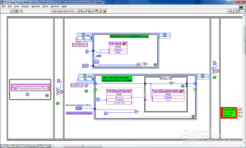
I would like to reset my memory block to all zeros (only once) using the FPGA code. In my past experiences, it did not by the FPGA e/s 'IO done Module\Initialization' NŒUD. To compensate for this, I used a SCTL that passes through each address of the memory block and stores a zero. The approach works fine, but I want to save space since we will quadruple the size of the code in a few months.
FPGA: 7954r
I/o module: 5761r
Thanks for the research!
Hey Denn_Mann,
You should be able to set your memory to initialize to zero in the memory properties. Here is a link that should help you:
http://zone.NI.com/reference/en-XX/help/371599G-01/lvfpgadialog/fpga_define_memory_db/
Hope this Helps,
Doug B
-
FPGA block memory and Timing FIFO
Hello
I am trying to access the data of the memory block and a FIFO, both having an equal number of elements.
I'm trying to access the data must be coordinated with the waveform of a block of Xilinx, I use to deal with the elements of the FIFO and the memory block.
My block of Xilinx has a 3 clock offset cycle and one without a clock cycle lag, which can lead to my use of knots of late.
My question is, the output of an element of a FIFO occur in a clock or a clock set cycle? Also, I am aware that there is a delay of the output clock cycle
block of memory to hold data into account initial reading, which will lead to my choice of offset of 3 clock cycle. Just a handful to decide how much to delay the nodes to use.See you soon
Hi RichieA
If the function or if it is a FIFO, or a memory block is inside the recycled then timed loop function and of all that is on the inside must be executed in a heartbeat. Don't forget that when you compile you are actually programming and connect a gate array so when the compiler is running, it will try to create the FIFO or memory to be executed on a tick. If this is not possible, you should get an error in NI LabVIEW or in the compilation process. Here is a link with more information.
Single-Cycle timed loop FAQ for the LabVIEW FPGA Module
Concerning
R. Esteban
-
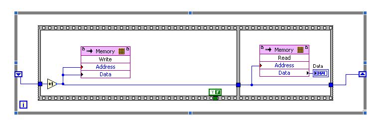
problem with a block of memory in labview 2009
Hi all
I have "ERROR: MapLib:979 - LUT4 symbol" during the compilation process (lots of errors like this), and I discovered that the reason of my problem is block of MEMORY.
To be sure that the problem is in this block, I did a very simple project in LabView 2009 (on FPGA Target PCI5640R) only with the use of this block you can see in the photo, as well as in file test_memory block.lvproj attached link: https://www.dropbox.com/sh/u87f1oihelmm4dq/Jo_6-bICSf
I have a problem with compiling VI with this block, and I have so many errors like:
ERROR: MapLib:979 - LUT4 symbol
"window/Thatcher/n_00000036/nSCTL_00000013_00000014/n_000000A3/cOutLoc<0>1.
(output = window/Thatcher/res000001ed_wi<2>) is the input signal
"window/Thatcher/res0000020d_wo<1>" that will be deleted. See Section 5 of the
Map a report file to find out why the input signal will become conveyors.or
ERROR: MapLib:978 - LUT4 symbol
"window/Thatcher/n_00000036/nSCTL_00000013_00000014/n_000000A3/cOutLoc<23>1.
(output = window/Thatcher/res000001ed_wi<25>) is an equation that uses
input pin I2, which no longer has a connected signal. Make sure that all the
the pins used in the equation for this LUT are signals that are not cut
(see Section 5 of the report file map for details on which signals were
adjusted).Entire report, you can see in the file report.txt on the attached link.
I would appreciate if someone could take a look at my problem with simple project and suggest me a solution.
I'm really stuck with my biggest project which need to have this memory block.
I'm looking forward to hear from you,
King looks
ING. Damir Hamidovic
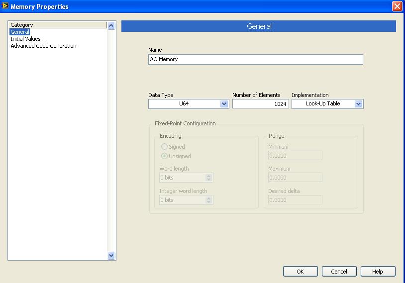
Hi all
I find a sollution to my problem.
In memory-properties-general-setting up, I changed the block to look up Table memory, and I compile memory.vi and run it successfully.
I did change as you can see on the picture:
Just, can you tell me is it all "bad properties" and limits the use of this type of memory (Look up Table) of the implementation?
King looks
-
Coregen memory when you use defined VI block memory
I currently have a problem when you try to compile a VI for my card Flex RIO (SMU-7965R). I have a sub - vi which contains a small instance memory set by VI (U16 X 256 elements) and a block of DSP48. This VI is instantiated 128 times in the top level VI. When I set up the memory set by VI to target the block of RAM in the FPGA, the compilation process is suspended during the generation of the nuclei (memory after ~ 45 min). LabVIEW treats each instance of as single block memory when executing coregen? I do not experience this problem when I set up the memory set by VI using LUTs. Any thoughts would be appreciated.
Thank you
Brian
Hi Brian,.
I believe that this compilation failure could be less related to the implementation of memory coregen, rather the memory of the way that is implemented in the lut and block memory on an FPGA. Lut are built through flip-flops and are perfect for storing information 100-300 bytes, while the memory block is segmented in a fixed size of 2 k RAM embedded. There are only a number of structures of block of RAM in a given FPGA and it seems that in your case that you use more of your resources block of allocated RAM. For example, in the 7831R if we tried to implement a FIFO in the maximum possible storage size block memory would be 81 920 bytes due to the limitation of resources.
The implementation of flip flop of the LUTs will allow the compiler greater flexibility in the use of resources in compiling because the size of the LUT is not fixed in the way that is a block structure of RAM. This is probably the reason why this LUT implementation is compiling successfully while the RAM block is not in this case.
Kind regards
Blayne K
Maybe you are looking for
-
Safari randomly opening new windows
Greetings, I searched the forum on similar topics and have tried all the tips I found. However, I've still not solved my problem. I have a MacBook Pro from 2012. My web browser, Safari, keeps randomly browser windows open. It's 'scam' Web pages for M
-
Satellite A200-10W - I can work only 1 hour of battery power
I bought the laptop A200-10w. The problem is the battery because when I surf the internet or use the word battery stamina is 1 hour. I turn off aero win, but there is no change. What can I do? Thanks, Marko
-
Windows xp will not update after re-formatting
I have a windows XP. I restored my computer back to factory new and now I am unable to load updates. I tried to loaqd SP1, SP2 and SP3. None will not load. You have a solution?
-
Continually 871122 WZC error.
-
How to determine currently logged-in - user?
I opened a command prompt with "runas/user: Administrator cmd" and I need to determine which is the currently logged-on user. Is this possible? Thank you.