demo FPGA of e/s problems
I tried to follow this demo , and when I get to the first part, adding the FPGA of e/s, I don't have any options to add in the window that is implemented. I have included a picture of the window that is implemented. This must of course simply be something that I'm just not.
You already have all the I/O resources possible for your target added to the project, so that the dialog box tells you there is nothing else, you can add. If you expand the folders ModA and mode, you should see these resources. For many objectives, adding the target to the project will cause the pilot interview target for all I/O resources and add them automatically to the project for you. The target used in the demo doesn't do this. This is probably what caused you confusion. If you remove inputs and outputs contained in the files and restart the add new e/s dialog box, you should see the e/s that you just removed as items available for selection.
Tags: NI Software
Similar Questions
-
SMU-7975R with FPGA Kintex-7 - LVDS problem
Hello
I developed a custom RIO FLEX module (Digitizer18, 0xAB66 - vendor id) and try to use it with the card 7975R-SMU-FPGAS (FPGA Kintex-7)
I have a problem, try output LVDS signal via aUserGpio (61) and aUserGpio_n (61).
These pins are not K7 capable clock, but I used this module FLEX RIO with SMU-7962R (Virtex-5 FPGA) where these pins are capable REGIONAL clock and it worked fine.
Kintex-7 it compiles without error, but I see no signals on the pins aUserGpio (61) and aUserGpio_n (61), although its switching State is ADC2_FSM.
Is it possible to use pins that is not capable of WHAT LVDS output or I am condemned to use MRCC clock or pins SRCC?
Thank you
My xdc file (aUserGpio (61) and aUserGpio_n (61) belong to the 18 Bank):
set_property IOSTANDARD LVDS_25 [get_ports {aUserGpio [61]}]
set_property FAKE DIFF_TERM [get_ports {aUserGpio [61]}]
set_property IOSTANDARD LVDS_25 [get_ports {aUserGpio_n [61]}]
set_property FAKE DIFF_TERM [get_ports {aUserGpio_n [61]}]# all unused pins Bank 18 are LVCMOS25
set_property IOSTANDARD LVCMOS25 [get_ports {aUserGpio [49]}]
set_property BUNCH SLOW [get_ports {aUserGpio [49]}]
set_property DRIVE 8 [get_ports {aUserGpio [49]}]
set_property BIO FAKE [get_ports {aUserGpio [49]}]...
part of my clip to vhd file (because it's too big and all other LVTTL logic works very well except LVDS):
attribute dont_touch: string;
Signal ADC2_CNV_buf: std_logic_vector: = '1';
attribute dont_touch of the ADC2_CNV_buf: signal is 'true '.OBUFDS_ADC2_CNV: OBUFDS
map of port)
O-Online aUserGpio (61)-Diff_p output (connect directly to the port of higher level)
OB-online aUserGpio_n (61)-Diff_n output (connect directly to the port of higher level)
I have-online ADC2_CNV_buf - the input stream
);....
process (LVDS_CLK) - 200 MHz
Start
If LVDS_CLK' event and LVDS_CLK = "1" then
ADC2_FSM case is
When s0 =>
If ADC2_CNV = "0" then
ADC2_timer1 <= (others="">' 0');
ADC2_timer2 <= (others="">' 0');
ADC2_CLK<=>
ADC2_READY<=>
ADC2_CNV_buf<= '1'="">
ADC2_FSM<=>
end if;
When s1 =>
If ADC2_CNV = "1" then
ADC2_CNV_buf<= '0'="" ; ="" ="" ="" ="" ="" ="" ="">
ADC2_RESET<= '1'; ="" ="" ="" ="" ="" ="" ="" ="" ="">
ADC2_FSM<=>
end if;
When s2 => ADC2_FSM<=>
When s3 => ADC2_FSM<=>
When s4 => ADC2_FSM<=>
When-online s5
ADC2_CNV_buf<= '1'="" ; ="">
ADC2_RESET<=>
ADC2_FSM<= s6;="" ="">
When-online s6
If ADC2_timer1< x"28"="" then="" --="">
ADC2_timer1<= adc2_timer1="" +="" 1;="">
on the other
ADC2_FSM<=>
end if;
When s7 =>
ADC2_CLK<= not="">
If ADC2_timer2< x"24"="">
ADC2_timer2<= adc2_timer2="" +="">
on the other
ADC2_READY<=>
ADC2_FSM<= s0; ="" ="">
end if;
When other => ADC2_FSM<= s0; ="">
end case;
end if;
complete the process;-the host uses the flank amount of DCO± to capture D±
process (UserGClk2, ADC1_RESET) - echo DCO2 clock
Start
If ADC1_RESET = "1" then
ADC2_READ_FSM<= s0; ="">
ADC2_BUF <= (others="">' 0');
elsif UserGClk2' event and UserGClk2 = '0' then - host uses the flank amount of DCO± to capture D±
ADC2_READ_FSM case is
When s0 => ADC2_BUF (17)<= not="" d2="" ;="" adc2_read_fsm=""><=>
When s1 => ADC2_BUF (16)<= not="" d2="" ;="" adc2_read_fsm=""><=>
When s2 => ADC2_BUF (15)<= not="" d2="" ;="" adc2_read_fsm=""><=>
When s3 => ADC2_BUF (14)<= not="" d2="" ;="" adc2_read_fsm=""><=>
When s4 => ADC2_BUF (13)<= not="" d2="" ;="" adc2_read_fsm=""><=>
When s5 => ADC2_BUF (12)<= not="" d2="" ;="" adc2_read_fsm=""><=>
When s6 => ADC2_BUF (11)<= not="" d2="" ;="" adc2_read_fsm=""><=>
When s7 => ADC2_BUF (10)<= not="" d2="" ;="" adc2_read_fsm=""><=>
When s8 => ADC2_BUF (9)<= not="" d2="" ;="" adc2_read_fsm=""><=>
When the s9 => ADC2_BUF (8)<= not="" d2="" ;="" adc2_read_fsm=""><=>
When s10 => ADC2_BUF (7)<= not="" d2="" ;="" adc2_read_fsm=""><=>
When s11 => ADC2_BUF (6)<= not="" d2="" ;="" adc2_read_fsm=""><=>
When s12 => ADC2_BUF (5)<= not="" d2="" ;="" adc2_read_fsm=""><=>
When s13 => ADC2_BUF (4)<= not="" d2="" ;="" adc2_read_fsm=""><=>
When s14 => ADC2_BUF (3)<= not="" d2="" ;="" adc2_read_fsm=""><=>
When s15 => ADC2_BUF (2)<= not="" d2="" ;="" adc2_read_fsm=""><=>
When s16 => ADC2_BUF (1)<= not="" d2="" ;="" adc2_read_fsm=""><=>
When s17 => ADC2_BUF (0)<= not="" d2="" ;="" adc2_read_fsm=""><=>
When s18 => ADC2_READ_FSM<=>
When other => ADC2_READ_FSM<= s0; ="">
end case;
end if;
complete the process;
ADC2_DATA<= "00000000000000"="" &="" adc2_buf="">I've made a few changes to TestCLIP.fam:
...
[FlexRIO-K7IOModule]
DefaultCLIP = TestCLIP
VccoLevel = 2.5...
And my xdc file now looks like this:
# Set the voltage from Bank to Bank 18.
#set_property IOSTANDARD LVCMOS25 [get_ports-filter {IOBANK == 18}]set_property IOSTANDARD LVCMOS25 [get_ports {aUserGpio [*]}]
set_property IOSTANDARD LVCMOS25 [get_ports {aUserGpio_n [*]}]
set_property IOSTANDARD LVDS_25 [get_ports {aUserGpio [58]}]
set_property IOSTANDARD LVDS_25 [get_ports {aUserGpio_n [58]}]
set_property IOSTANDARD LVDS_25 [get_ports {aUserGpio [67]}]
set_property IOSTANDARD LVDS_25 [get_ports {aUserGpio_n [67]}]Now it's working.
-
Possible to use the main clock FPGA as a basic Source of time for the NI 9234?
Hello
I am running a NI 9234, and NI 9222 module on a cRIO-9114 chassis with a real-time 9022 controller, data acquisition on the 8 channels on the full sample rate, using the FPGA.
My problem is the synchronization of the data, where the NI9234 is usually a late acquisition, compared to the NI9222. I tried manually delay the NI9222 to take the first samples, but so far without success.
To solve this problem and also to ensure a rate of data more comparable on both cards, I was wondering is it possible to create a Source of time Base master for the NI9234 WITH THE FPGA (opposite to import from another NI9234 or similar module)? The NI9222 I already provide with sampling of the impulses from the FPGA (as expected with this module).
Another issue would be the characteristics of the exact chronology of the two modules, including in terms of synchronization between the beginning of the acquisition and the first samples of data. I couldn't find any information about it...
Thank you in advance,
O Hoppe
Hello!
I've never heard of a possibility to use a time base FPGA with a module of Delta-Sigma.
But I think that the question should be what has not worked to delay the signal and how you did it. Have you read this article?
How can I compensate for delays of different group with the C Series Modules in LabVIEW FPGA?
http://digital.NI.com/public.nsf/allkb/74EB238E1BCADD528625735300681A7DCan you give a more detailed description of your trial to delay acquisitions? Can you provide a code example?
Best regards
Christoph
-
Hi all
Please, for the love of God can someone take a look at the attached FPGA project, I hit to the top and tell my why it is that whenever I run, as soon as he's trying to read/write on the host computer, it returns error-61046? A screenshot of the error is included in the attached .zip file.
I made many programs FPGA before with no problems, while using the same FPGA and FlexRIO module and never had this problem. If I run an example program it works fine so I am confident, that the error lies in my programming, I can just see where!
As you can see all the clocks are internal and appear to be configured correctly according to the example programs and other programs FPGA, that I have done before, so I'm puzzled. I hope that it is just my stupidity and lack of coffee.
Congratulations in advance.
Mitch
The pilot FlexRIO comes two CLIPs for the 5781. At ' a "NI 5781 Sychronous system" OR 5781 "VIDEO CLIP.
The "NEITHER 5781' is what originally delivered with the FAM and is always delivered with the driver for legacy purposes. I would discourage the use of this CLIP because it uses regional clocks for IO Module clock 0/1 which limit the amount of fabric that can be driven by these clocks to the fabric available in the respective region of the FPGA. The advantage of this CLIP, it's that the ADC and DAC can be clocked at different rates through a clock divider that exposes the CLIP.
The 'NI 5781 Sychronous system"CLIP is what is recommended for all new models. It uses a world clock which can target tissue in all regions of the FPGA. This CLIP uses the same clock to drive the ADC and DAC (IO Module clock 0). IO Module clock 1 is not used in this CLIP.
If you used the sychronous CLIP system and always a logic had driven out by IO Module clock 1 it that would explain why you received the error of non-response from IO Module clock 1 is left connected in the sychornous CLIP system.
-
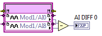
Differential using NI 9205 using FPGA
If I need to make a differential measurement, do I need to subtract the corresponding entry to this?
(This could be executed on FPGA)
Are there problems (such as clipping) if my input range is small, lets say ±200mV but my IO is floating in, say, 3.0V on AI0 and 3.1V on AI8?
To take a differential measurement with FPGA, you first need to go to your project and right-click on the module and access its properties. You should see a list of all your channels, as well as their input range and terminal mode. The value the + channel for everything that match you are eager to use it as DIFF and file I/O node just to the canal +. You don't have to do a manual removal.
Not expect problems with the behavior you described.
-
Open vi FPGA gives error xnode (Lv 8.6) (not executable)
Hello
I wrote my description of the error also here: http://forums.ni.com/ni/board/message?board.id=280&message.id=5055&jump=true#M5055
When using "run vi on the development computer" I get an error broken pointing me to the "open FPGA vi function", the problem
be 'an xnode object is not executable. I have not found this problem under discussion anywhere, I tried uninstalling FPGA and Rio soft.
and resinstalling, but not help. All ideas are welcome.
Thank you
Staffan
Hello
JMota wrote:
"Here's something to try. I think that the configuration of your FPGA target to run on the development computer (with simulation of IO) will not work if you try to run your host VI on RT. test by dragging the VI to my computer and run it from there. Altenatively, you can reconfigure your FPGA target for not performing on the development computer (what used to be called emulation).
Hope that explains why the VI has broken. »
And it solved the problem - works fine now - if this issue is resolved.
Staffan
-
FIFO of DMA beteen switching channels after sends FPGA
Dear community,
I read 8 AI with the CRIO high frequency corresponding to 8 sine waves of resolvers. Also, I do operations in the FPGA and passing to the RT host 2 FIFOs. One is called resolvers with these 8 channels and the other is called speed and accel. who has 12 channels with 4 angular positions, 4 speeds and accelerations 4 in that order. When I read the two FIFO with the host I wait for the PEPS have enough elements. I also put the time-out of the FPGA-1 to avoid problems altought I know very well what to select. The problem is that when I read with the host, the channels do not keep the original order I used to assemble in the FPGA and also it is possible to appreciate swithings between channels every few seconds so that the information is not uniform and robust. It is not possible to use the information if the channels do not change their relative position.
I have ideas to solve this and incrementing the RT frequency because it goes to the maximum of 60 Hz, where I expected much more.
Thank you very much.
Concerning
Enrique
EnrikDS wrote:
Hello
attached are two images to explain what settings I use to configure FIFO. We can concentrate on speed FIFO:
-Depth confgured to: 120000
-Number of items in a read statement: 1200
The FIFO can also be configured in the Project Explorer, in fact, I'm not sure if the depth setting configured in the block diagram means the same as the parameter
"Asked number of items" that appears when you double-click in the FIFO to the Project Explorer, the value is 4095. Other values are:
-Target to the host
-Data type: FXP (64-bit, 32-bit)
I hope this helps. Thank you very much for your support.
Enrique
When you configure the FIFO since the project you define how much space FPGA to be used for the FIFO for buffering before data are duplicated in the FIFO of RAM defined by the property node.
Have you tried to set the expiration time of the FPGA FIFO entry to 0, that would be a FIFO with loss. You can use the FIFO. GetNumberofElementstoWrite to ask how much space is in the FIFO and write only when you have 8 to 12 free items.
-
So for what I need to do the FPGA is send fixed point numbers ± 20, 5 to a chassis of 9146 OR ethernet with an analog voltage NI 9264 as modual output 2, he sends - 10-10 m Volts out in a thread. I create an FPGA VI and have problems, so I said delegate my code in the simplist components and finished with the code in the attached photo. The problem is that the sending of information to the Mod2/AO4, channel, I send you, takes an infinite time and the signal does not get sent (I have a thread to check if the voltage is set through). What I found, it's the right way to send information on the chassis, it works with Boolean values. Is there something special I need to do to fixed point?
Thank you for your time
Mitchell Wörner
-
FPGA: 'the bitfile signature does not match." Any changes made
Hello
I have a project involving a cRIO9082 and its FPGA target. My problem is that I keep having to recompile the FPGA build, even when I have not changed anything. Is there a setting I'm missing here?
Thank you
Ok. It is difficult to say why his need to recompile, but the quick fix is here: Configure open the VI FPGA to open bitfile, not the VI (you will need to create specifications to build on FPGA, integrate the bitfile VI).
With regard to the reasons why he needs to recompile every time:
-Are you moving this code between different machines (via control code source for example)? Different version (SP) of the LV or FPGA module may be the reason.
-Make changes in the subVIs of your FPGA VI main?
-Do you have screws that serve both on FPGA and RT?
-
How can I change the clock from the fpga to the entire code
Hi I am new to the labview and using 8.6 demo (fpga modules in real time).
I developed some codes to practice and you want to change the clock freq 200 MHz of 40 M for all codes.
I mean how to use clock derived for my vi.
You create a clock FPGA derived from the "clock of 40 MHz on board" in the project manager.
Then in the properties for the FPGA, you can select 'Top level Clock '. High level for the FPGA clock can be that what follows: 80 MHz, 120 MHz, 160 MHz, 40 MHz, 200 MHz
-
Hello
I just started to use LabVIEW FPGA and have some problems with the acquisition of signals. I set up a test project where I try to the issuance of a signal using a NOR-9263 and collated the signal using a NOR-9215. In addition, I measure a signal created by a signal generator sine. During the measurement, I get unexpected values (see attatchment). I think I get into trouble with the FIFO storage. What is my failure?
Concerning
Daniel
My first guess is that you run into a situation where once from time to time, the number of items to be read from the FIFO is not a multiple of the number of outputs to Decimate 1 d Array. When this happens, you will lose data and the first item next FIFO reading doesn't match the first chain, so you will get incorrect values on the chart. Try to change your code so that when you do the reading of FIFO, it reads that multiples of the Decimate 1 d table size, not to mention that this number should also be less than or equal the number of elements to read in the FIFO (as you already).
EDIT: also, you must make sure that the FIFO write never times out. Now you're ignoring this value. Chances are, it won't expire here, but if this is the case, which could also cause problems because you could write only some of the channels before it fills, which still move channels.
-
FPGA compilation I get error & quot; ERROR: ConstraintSystem:58 & quot;
I use the Xilinx LogiCore IP generator for generating DSP IP for my FPGA.
The problem is that the names of the generated components are for a long time.
On the Web site or http://digital.ni.com/public.nsf/allkb/F810E4289A420FE68625796600764C66
He described a problem very similar to what I have ID issue 309260 "compilation error (ERROR: ConstraintSystem:58) when compiling a LabVIEW FPGA VI which contains a generated from a DSP graph VI.»
I followed the suggestions and changed my IP to names such as 'A' and 'B '. As a first step, that it did not work, only to spend the entire project to another shorter path of directory did this job.
Now, when I regenerate the IP address of 'Tools' > 'FPGA Modules' > "Regenerate the node IP" this will rename my IP with an additional random name at the end. So, if I look in my case not only that I have "A.vhd" but now, I'm also having 'A_F27AB4F7464E508DCCB219B2C4271B18.vhd '.
It's very repetitive, and you should be able to replicate that.
It's havoc with our software and with our software process control tool. Our database of software can accommodate only names of files of a certain length, and this violates. Also, I now have files with the exact same content but with different names.
Do you have a fix for this problem as stated on your website?
Kind regards
I ended up using LogiCore externally. If you do a search in your LabVIEW FPGA tools folder, you should find "\Xilinx12_4\ISE\bin\nt\coregen.exe" (in the case of the specific version of Xilinx tools you have), it's the Xilinx Logicore exe without the National Instruments candy wrapper.
I created all of my external LogicCore to LabVIEW (it actually makes life easer, the LogicCore tool has a better Manager to track all your IP LogicCore in any case) and then used the IP LabVIEW nodes to access the intellectual property.
This has prevented the long names, and now I can better handle the INVESTIGATION period because I can put the code in a folder I want without breaking of LabVIEW.
-good luck
-
Hey guys, I'm new on Muse so this may be a simple solution, but at the moment, nothing seems simple.
I try to get my footer works correctly, but when I check the box at the bottom of page content preview as being pushed much closer together it appears in my design.
I experience problems with this before: content does not end up anywhere near where I place in my drawing.
What I've noticed, is that, although I am working on a breakpoint 1366 when design, there are visible guidelines for my next breakpoint (768) on the Web and that's where my content seems to align to. Why would it be?
In Muse nothing automatically aligns to anything and especially not of 'guides '.
My proposal: create a small and simple demo site, which shows your problem, download this. Muse Dropbox folder or something like that and post the link of download here. Doing so will prevent us from guess without end and assuming that, because you are faced with the question, can have hundreds of reasons.
-
Apple TV (4th Gen) App store (Singapore) does not work after last update tvOS 10
I tried a hard reset or empty everything and re-updated my Apple TV.
However, I am always faced with the same problem to have 'white' pages or does not respond to 'Top Charts', 'Categories', 'Search' and 'purchased apps. The only page I can access will be the page 'recommended '.
Just tried a restore through iTunes. It always behaves the same. I have also this checked the dealer NuBox apple their game demo is having the same problem as well.
Can we all here in Singapore with the same generation of gen Apple TV 4 having this same problem after TVOS 10 updated? Would it be a bug in the new TVOS?
I have exactly the same problem of hv too... apple told me something wrong with Apple TV Apps Store for some regions, including Singapore. Waiting for hotfix
-
Event navigation response is Slow
Hello
I have download a demo interface to illustrate a problem I encounter.
I use a control tab and 'Buttons OK' to change the tabs.
The appearance of the 'OK' button is changed by pasting images of Microsoft Visio, through the button right click-> Advanced-> customize.
Clicks on the "OK" buttons are captured using the "change value" in a "Structure of the event.
The problem is that sometimes an "OK" button needs more 1 click to work. In the original interface that has more decorations, the buttons "OK" a lot... a lot of clicks people need to go to another tab.
What is more, the tabs are not clickable, when the program is in "Run" mode
What should I change?
Thank you.
nikosfs wrote:
If the labels are not at the top of the tile, they are not visible. But if they are on top, they exclude a clickable area. Then?
Use the Boolean text and hide the label
nikosfs wrote:
If I make the buttons bigger than images, I need to make it transparent, but I don't know how I can do.
You must import photos into the button, not the decoration elements. (see button on page 2, that I modified in the VI attached. I have not hcange anything else...).
nikosfs wrote:
I am attaching the file vi once again, this time with the while loop. It does not seem to occupy 50% of the CPU usage, but my interface original, does have a similar code.
You wired probably a zero for the timeout.
Also, for the latch action buttons, terminals belong in the respective events. Also note the coercion. Enum constant diagram is of the wrong type.
Maybe you are looking for
-
NB305-N600 Fn F6 and F7 work (brightness) but wrong way autour?
Hi all I recently bought this netbook for my aunt and I spent the last two days trying to understand this issue I'm having. PROBLEM: When you press the function key + F6 / F7 brightness does the opposite of the button. for example, the brightness by
-
Satellite P500 - screen remains blank after updating BIOS 2.90
I installed the new WOOD update through the station of service and after restart, the screen remains blank (out of service)? Any suggestions?
-
Blocked C4580. I can't remove the last print queue doc
Wi - Fi works very well, analysis and test page works well. a single document is blocking the print queue. I tried to remove it again and again. It's a web page, I think. It says "delete", but nothing happens, it will not disappear. Any suggestions?
-
I have a laptop Acer Aspire 5349. I just put in a new hard drive and I bought the Acer recovery
I put the system disk in my cd drive, but it does not start. I looked in my bios and I see my cd listed and I chose it to start up. Does anyone have the answers. I worked on this for 2 days and I am at my wits end at this point. I even recorded files
-
not find don't win xp disk hard there is no drivers