E/s FPGA pin delay
I have a question about a FPGA project I'm developing.
I use a digital RIO NI PCI-7813R, objective and Module FPGA 8.6.1
I implement a SPI bus, master.
I use a state machine in a single loop of Timed Cycle. (about model on one of your examples IP)
I'm running the loop at 20 MHz, which produced a clock of 10 MHz SPI bus data.
I send you the data in 8-bit bytes delivered by a FIFO of the host.
Similarly, I return data bytes of 8 bits of the host by using a different FIFO.
I have no problem sending data, generate all the select chip and data impulses on my desired clock edges.
It's manual clean and perfect as seen on a scope / Logic Analyzer.
When I read data from i/o pin however I have found unexplained behavior.
It is this: the data seem to be trolling by two read operations.
When I read the axis of I/O data to the specified limit of the clock that I generate.
I found that the data were two bits shifted to the right, i.e., deferred, one on the scope / Logic Analyzer.
I did a work around by two pins I/O multiple read operations in time of the gap between the data bytes.
There are no generated clock signal and no data valid on the I/O pin at the time of these two read operations as testified to by the scope.
And now the data received matches perfectly to the one sent.
I can only assume that there is some kind of pipeline or delay inherent in the IO read operations. (at higher clock rates)
I suspect that there may be something in the optimization performed in the compilation of the structure of the SCTL the cause.
I had found it, sometime before in my development, that data has been little offset from 1 only one position.
I think it was at a slower pace of global clock.
I also ran the same state machine in a classic logic expect everything in a loop with an FPGA, to produce a much slower system
and I found that there is no delay at all.
I don't see anything in the configuration i/o pins that can affect this. (I turned off arbitration)
Similarly, I don't see anything in the documentation that could refer to this behavior.
8.6.1 of LabVIEW FPGA Module Known Issues (http://digital.ni.com/public.nsf/allkb/F6B5DAFBC1A8A22D8625752F00611AFF)
I'm about to use and deploy the code with the solution because it seems to be reliable.
But I am at a loss to explain (in my documentation of the code) why it is necessary
or how to solve this problem if the compiler changes.
Do you have any suggestions?
I think that what you run is that the number of sync records used with the digital I/o. If you right-click on the I/O item in the project and select the property page, you should see an option for number of registers for output and output enable synchronization. These settings are global settings for this I/O item that will be the effect on all nodes of the I/O writes to this point of I/O. Similarly, if you right click on the e/s on the schema node and select Properties, you should see a setting for number of registers of synchronization for playback. This setting is specific to this instance of the node for this element of I/O and can be configured differently for each node in the diagram. The effect is that each sychnronization registry will delay this beating of a clock signal. These records are inserted to prevent the problems of metastability and ensure that you always have signal levels valid when the IO is sampled on the edge of the clock. There is a problem whenever the producer and the consumer of the signal are market off different clocks, or at different clock rates. If the external device drive your digital inputs work synchronous clock you are producing, you can eliminate the registers of the synchronization. However, you must perform an analysis of delays in propagation of the signal between the two devices and make sure that all the settings and hold times are always met before. In the end, I think that the easiest and most robust solution will be to compensate for delays in sync in your code as you do already. I hope this helps clarify things.
Tags: NI Software
Similar Questions
-
meter in the sbrio limitations
I received conflicting information on the width minimum counter on a sbrio pusle.
The documentation specifies a minimum 100 ns pulse still dig it can be done at 40 MHz.
Why is it not possible to count impulses pretty accuratly using a loop of an individual program timed to 25ns impulses which are separated at least 25 ns.
I do not have 100% of all counted impulses but need to get the best of them.
What is the cause for the limitations, I haven't read any of the sctl?
Hi all
Another emphasis of the number 10 MHz is that it represents what can be accomplished with a common wiring for Single - Board RIO and using 5V signaling rates and operates all 110 DIO lines at the same time (worst case scenario). The user guide for Single-Board RIO gives a schematic representation of the circuits between the DIO and FPGA pins and discusses the characteristic impedance of the traces on the map (60 ohms). Given this knowledge, you can see the part number of the switch bus single board onboard, which further investigation part shows will ensure only 5V to 3.3V translation at speeds of up to 10 MHz. If the external signaling levels are 3, 3V native FPGA, the throttling of the bus switch would become less of a problem. Given a combination of good matching impedance of the trace to the impedance of the cable (use the cable recommended in the user guide), 3.3V report levels and carefully select what DIO lines operate simultaneously, you can get bandwidth signals significatly higher for the FPGA with signal integrity is good. Come on, I dare a range of 30 to 35 MHz consistantly.
The bandwidth of traces connections between the fitting and FPGA is a different specification for sampling frequency. It is true, as fast as you can get the a VI LabVIEW FPGA to compile reliable, enjoy the signal in LabVIEW FPGA (60 or 80 MHz for example). Fastest sampling will give you the best temporal resolution when the edges occur, but does not mean that you can communicate reliably via a digital Protocol to 80 MHz. Traces will always limit to how signals are transmitted to and from the FPGA.
Hope this clears things up,
-
Delay FPGA using a derived clock
Hello
Probably a simple answer to this. I have the PXI-7813R that has a clock of 40 MHz I database I need to create a delay time of 488nSecs in my code. Unfortunately with 40 MHz, I choose 475nSecs or 500nSecs. If I use a clock derived from 80 MHz I get a 487.5 delay which is very close to what I need. However, if I change my level above 80 MHz clock I get various offences of timing during compilation. Is there a way to keep the clock of 40 MHz top-level, but use the clock of 80 MHz for a time delay?
Thank you
Andy
Hi Andrew_Quick
Do you use this clock derived on a SCTL? I did some research on your question and find Knowledge Base article next talks a little about the way in which the clocks derivatives works with the SCTLs and in section shifts, there is a note that some codes can compile not at higher rates at 40 Mhz due to the time constraints of the FPGA , so I think that you should check that you don't have warnings or suggestions for when creating your clock derived to your target.
Even if you select the clock 40 MHz as the top level, if you select the clock of 80 MHz for the timed loop, the compiler will have to adapt all functions in the FPGA, and according to the error that you get that may be causing the violation of timing.
Hope you find it useful!
-
Can damage the FPGA module if I connect accidentally two pins writing together.
My current configuration has a PXI chassis with two FPGA modules. Each FPGA module has an adaptation Module 6581 on that. I would like to test the signal through my system path by having the user to move some cables that would be a reason for a return to the other looping FPGA.
I fear, however, the risk of the user is not correctly as shown and somehow a channel available in writing that connects to another channel write-enabled. This damage to the FPGA or adaptation modules?
Hi Brian,.
Your concerns are correct. We never want to connect two pins that are output voltage. If two pins are outputs digital mistakenly connecting them together may damage one or both nodes in output since there is nowhere to flow the potential.
It is well to connect to two pins that read a voltage. If both pins running entry digital (reading of the pins), as there is no risk, nor pin would be likely to be damaged.
-
Pin configuration of e/s for an FPGA
Hello
I have a 7830R FPGA which has "DIO" pin on this subject. I would like to cofigure some of these pins to be entered and others to be taken out. Where to define what they must be configured as?
Cheers, AlecThere's FPGA IO nodes property that you can use to "activate the output.
-
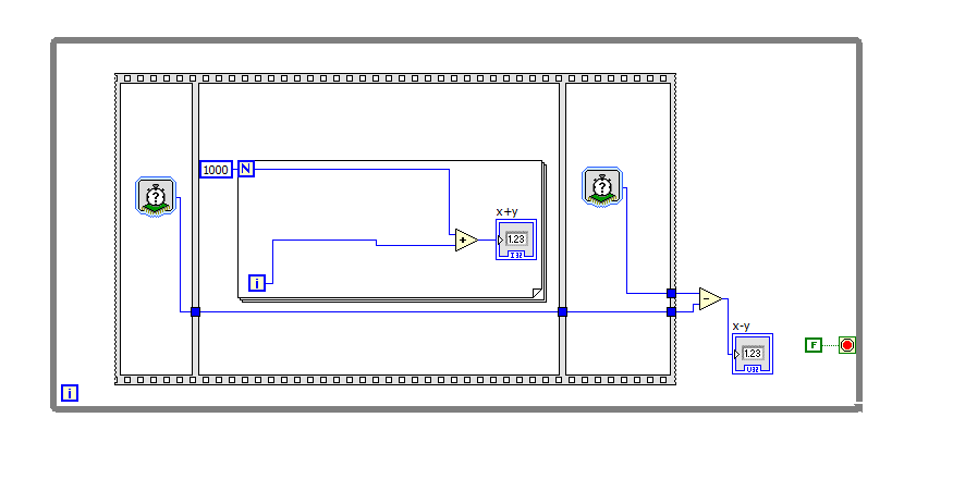
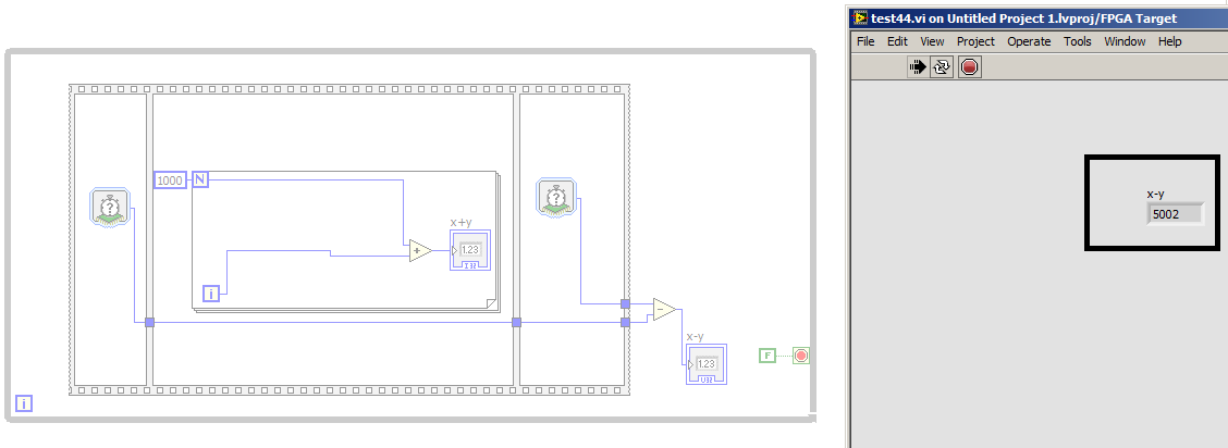
example simple + huge delay + fpga
Hi Member
I'm trying to caclute number of clock for this example caculate, the delay for the ' ' «for loops with 1000 run»»»
After complition process the vi was executed on fpga and read the number of cycles in the pc with the real time and the number of clock was 5002 clock as shown below
What is c?
is their any wrongdoing in my vi
mangood wrote:
So if a system (add many components, sub) and put this system inside the ""while loop"
Inverse of the period of the loop will be the frequency of the loop. Or frequency system is true!
-----------------------------------------------
I'm sorry for the stupid question, but my work on the architecture of the systems so these parameters is crucial and important for me.
I left my old job on tool company xilinx ISE because the design of the system to take a lot of time so I now moved into labview fpga, its amazing especially in the optimization process, but the clock Concept here is very weak and totally confused.
It's a different clock concept that most use of FPGA designers, it's true (I am trying to learn about it at the moment I'm doing some work software - C, not LabVIEW - on a processor clocked inside an Altera FPGA). For a normal programmer it makes sense - it works just like it does on a desktop computer. On a desktop computer you do not need to know how fast the processor is, you just need to know how long it takes your code to run.
I don't know what is the distinction between the loop and frequency of system for you. There could be other components of the system that are running at a different frequency that you don't see, but are required by the LabVIEW environment (for the acquisition of data or communication with the host processor), but your code inside the loop runs at the level of the loop which can be measured with the number of cycles.
-
How to pass the FPGA DI implemented FPGA vi pins to RT impemeted vi
Hello
I use two "FPGA sbrio' DI to implement the data RS232 (RX, TX)
I'm now able to communicate with 1 deveice with this Protocol.
I want to communicate with 3 device (in parallel) in the FPGA thought, copy the following (RS232) code.
the pins are coded inside main code main FPGA RS232,
"I have three RT vi to communicate with 3 different devices using this code), but now I want to communicate with them simultanouly. so, how can I configure the FPGA through pines
so I need to each vi to specify DI pins to connect with via rs232, how do I do this?
Kind regards
SASA
Your architecture must change a lot to get it right. You should read the data through a FIFO instead of use the interface on the front panel.
I recommend that you change your VI so that it is a Subvi. Make sure it is reentrant. For starters, you can pin Numbers and a reference to FIFO. Then in your main VI, you call just this VI three times with different constants at the entrances to designate different pins to use. Use a DMA FIFO for read data that must be sent with some additional data to tell you which bus to send to. Then, you pass just the data along the via FIFO belongs to the port you are writing.
-
LV FPGA delay seen between subsequent of the SCTL
Hi all
I'm developing a customized with a FAM 6581 LV FPGA and a FlexRIO SPI. I need to communicate with the microcontroller requires that I write 16-bit data on a clock edge followed 8 clock cycles for data through the process in the Aluminum and the clock microphone on the rise. Then I need to provide others 16 clocks to clock on the 16-bit result. I did initially with 3 single-Cycle timed loops, one for each section. Am I on the references of the IO of each SCTL following SCTL to get the correct data stream. When I look at signals with a Logic Analyzer I see each section works correctly, but there is an approximate time 504ns between each section of the code. I was expecting sort, perhaps only a single clock cycle delay between s SCTL but not much. Anyone got any ideas on what could be the cause and how can I fix this?
Thank you all,
Nick
Instead of using several distinct SCTLs, consider using a SCTL as a state machine that can handle these three steps.
-
problem of delay FPGA can understand
Hello I have labview pci virtex 2 card in the computer and try to implement DMA from the host to the fpga (I use a clock of 200 mhz, which is the first of 40 MHZ with pll multiplier)
but every time I have an error of period not comply with the requirements of compilation happens that I can't understand how to fix it
I tried changed settings tick and insert the delay loop, but does not change the error
I have attached the results of error timming
can I get help on hw to solve?
Ghattas.Akkad wrote:
If a fast clock should not be better then a slower?
What do you mean by "better"? Faster, the clock, less you can do in a clock cycle. Your code uses a single-cycle timed loop, which means that the entire interior of the loop must run within a single clock cycle, and there is also a lot of logic in it to run at 200 Mhz. A fast clock is not better than a slowdown, if it is not possible for the code to run at the faster clock speed. Why did you choose 200 Mhz?
It is also unnecessary for the structure of the sequence, even if this is not bad no matter what.
-
Newspaper delayed pine on when full beginning upward
Windows 8 and 8.1. Full boot (e.g. restart or start without Fast Start Up)When I use PINS to connect my laptop, it will freeze up to 30 seconds and return to the lock screen, after the freeze in 30 seconds, I see the 'welcome' and to go to my home screen.
Anyone know what is happening here?However, normal password log on will not have this problem. So I guess that there is some problem with PIN and photo log.Hello Lin
I had the same problem and managed to fix it by changing the startup type of the service Credential Manager (VaultSvc) Manual to Automatic.You can launch the configuration of services with services.msc window.Good luck, Pascal -
Generation of PWM in FPGA pulses with nano seconds
Hi guys,.
I work with myRIO FPGA.
I have seen a few examples to generate PWM pulses in the FPGA target with the help of timed structures. Timed structures can contain the frame in the sequence structure flat with time control less than 1 micro second (1 MHz).
But I want to generate impulses PWM digital pins in hundreds of nano seconds.
I saw datasheet of myRIO - 1900. It can generate a frequency up to 40 MHz.
I need the pulses on the order of 10 MHz.
Can someone help me how to generate pulses on the order of 10 MHz PWM?
Hi fires,
the FPGA can use "ticks" aka clock pulses for delays.
As your impulses are of the order of 4 ticks, you could use simple statements waiting!
-
VG224 and Verifone xx810 chip and pin component terminal modem
Hi members of the community.
I have a very specific problem I'd appreciate help with if anyone else has experienced this or something similar.
We have a VG224 that provides analog lines for fax machines mainly on our campus. Recently, we had our Department of finance use machines to chip and PIN on these connections. Previously, we used streamline machinery, and they connect properly.
The specific case I have is a Verifone vx810 machine which is connected to a VG224. The Verifone unitis able to deal with success and to authorize a transaction, but it cannot complete a download batch process or a TMS. I talked to the support company that rent us machines to and identified that the computer uses the following baud rate, bits of parity and stop for 2 different operations:
For transactions: 2400 baud, parity/stop 7e1 (this works)
For the batch upload/TMS: 19200 baud, parity/top 8n1 (it does not).
In the case of the upload of batch/TMS, the machine connects, gets a connection to the remote end to the PSTN for about 10 to 20 seconds, then he tears because the modem negotiation fails. I've read various articles on forums CIHI and others say that data rates high speed can be a problem for the VG224, but nothing to suggest a problem with 19200. I also tried installing on an ATA186 and ATA showed the same symptoms, so I am inclined to think that this isn't just a firmware issue or bug with the VG224. I tried 3 different chip and PIN machines of the model vx810 and all have the same symptoms.
Here's a copy of my current VG224 config. The VG224 is recorded in the CUCM via SCCP.
version 12.4
no service button
horodateurs service debug datetime localtime
Log service timestamps datetime localtime
no password encryption service
!
hostname vg224
!
boot-start-marker
boot-end-marker
!
forest-meter operation of syslog messages
logging buffered 4096
!
AAA new-model
!
!
AAA authentication login default local radius group
the AAA authentication enable default
AAA authorization exec default local radius group
failure to exec AAA accounting
action-type market / stop
RADIUS group
!
!
!
AAA - the id of the joint session
clock timezone GMT 0
clock summer-time recurring UTC 4 Sun Mar 01:00 4 Sun Oct 02:00
IP source-route
IP cef
no ip domain search
!
!
No ipv6 cef
!
stcapp ccm-Group 1
stcapp
!
stcapp function-access code
!
stcapp speed dial feature
!
!
voip phone service
Modem passthrough codec g711ulaw nse
!
!
voice-card 0
!
username
password Archives
The config log
hidekeys
!
!
!
interface FastEthernet0/0
no ip address
automatic duplex
automatic speed
!
interface FastEthernet0/0.644
encapsulation dot1Q 644
IP 10.1.160.4 255.255.255.0
!
interface FastEthernet0/1
no ip address
Shutdown
automatic duplex
automatic speed
!
default IP gateway - 10.1.160.1
!
IP forward-Protocol ND
IP route 0.0.0.0 0.0.0.0 10.1.160.1
no ip address of the http server
!
exploitation forest installation local6
interface FastEthernet0/0.644 source journaling
logging
SNMP-server
RO community SNMP server location
!
Server RADIUS
auth-port 1812 1813 acct-port host Server RADIUS
auth-port 1812 1813 acct-port host RADIUS 3 server timeout
RADIUS server key
!
control plan
!
!
!
voice-port 2/0
cptone GB
initial delays of 60
timeouts interdigit 60
timeout infinity ringtone
activation of the caller ID
!
voice-port 2/1
cptone GB
initial delays of 60
timeouts interdigit 60
timeout infinity ringtone
activation of the caller ID
!
voice-port 2/2
cptone GB
initial delays of 60
timeouts interdigit 60
timeout infinity ringtone
activation of the caller ID
!
voice-port 2/3
cptone GB
initial delays of 60
timeouts interdigit 60
timeout infinity ringtone
activation of the caller ID
!
voice-port 2/4
no echo - cancel enable
cptone GB
initial delays of 60
timeouts interdigit 60
timeout infinity ringtone
activation of the caller ID
!
!
CCM-manager cisco Protocol fax
CCM-Manager config server
CCM-Manager config
CCM-Manager local FastEthernet0/0.644 SCCP
CCM-Manager sccp
!
!
SCCP local FastEthernet0/0.644
SCCP ccm
version ID 1 6.0 SCCP ccm
2 identifier version 6.0 SCCP ccm
identifier 3 version 6.0 SCCP
!
SCCP ccm Group 1
associate the ccm 1 priority 1
associate priority 2 CCM 2
associate the ccm 3 priority 3
!
transcode dspfarm profile 1
associate the PCRS application
!
!
voice pots Dial-peer 999200
Service stcapp
port 2/0
!
voice pots Dial-peer 999201
Service stcapp
port 2/1
!
voice pots Dial-peer 999202
Service stcapp
port 2/2
!
voice pots Dial-peer 999203
Service stcapp
2/3 port
!
voice pots Dial-peer 999204
Service stcapp
port 2/4
!
!
!
Line con 0
line to 0
line vty 0 4
!
NTP server
NTP server
end
And a version of the show of the vg224:
System to regain the power ROM
System restarted at 14:30:34 CEST Wednesday 9 may 2012
System image file is "slot0:vg224 - i6s - mz.124 - 22.T5.bin".
Cisco VG224 processor (R527x) (revision 4.1) with 119808 K/K 11264 bytes of memory.
Card processor ID FHK1432F2CC
R527x CPU at 225 MHz, 40, Rev 3.1 implementation
1 voice module 24 analog FXS edge V2.1
2 FastEthernet interfaces
Configuration of DRAM is 64 bits wide with disabled parity.
63K bytes of non-volatile configuration memory.
The system of fpga version is 250027
The system of readonly fpga version is 250027
Option for fpga system is 'system '.
62496K bytes of ATA Slot0 CompactFlash (read/write)
Configuration register is 0 x 2102
This problem is really driving me crazy, if anyone can shed some light on what is perhaps the root cause of that I would be very grateful.
I would say probably yes, devices compatible PCIDSS circulating on the network IP would be the way to go and that is something that we work, but currently we have units that can communicate using analog telephone lines.
OK, PRI is clean so you must relay setup for connection of modem modem high speed work.
I would not waste time with CSPC and go immediately to SIP or H.323.
-
Possible to use the main clock FPGA as a basic Source of time for the NI 9234?
Hello
I am running a NI 9234, and NI 9222 module on a cRIO-9114 chassis with a real-time 9022 controller, data acquisition on the 8 channels on the full sample rate, using the FPGA.
My problem is the synchronization of the data, where the NI9234 is usually a late acquisition, compared to the NI9222. I tried manually delay the NI9222 to take the first samples, but so far without success.
To solve this problem and also to ensure a rate of data more comparable on both cards, I was wondering is it possible to create a Source of time Base master for the NI9234 WITH THE FPGA (opposite to import from another NI9234 or similar module)? The NI9222 I already provide with sampling of the impulses from the FPGA (as expected with this module).
Another issue would be the characteristics of the exact chronology of the two modules, including in terms of synchronization between the beginning of the acquisition and the first samples of data. I couldn't find any information about it...
Thank you in advance,
O Hoppe
Hello!
I've never heard of a possibility to use a time base FPGA with a module of Delta-Sigma.
But I think that the question should be what has not worked to delay the signal and how you did it. Have you read this article?
How can I compensate for delays of different group with the C Series Modules in LabVIEW FPGA?
http://digital.NI.com/public.nsf/allkb/74EB238E1BCADD528625735300681A7DCan you give a more detailed description of your trial to delay acquisitions? Can you provide a code example?
Best regards
Christoph
-
SMU-7975R with FPGA Kintex-7 - LVDS problem
Hello
I developed a custom RIO FLEX module (Digitizer18, 0xAB66 - vendor id) and try to use it with the card 7975R-SMU-FPGAS (FPGA Kintex-7)
I have a problem, try output LVDS signal via aUserGpio (61) and aUserGpio_n (61).
These pins are not K7 capable clock, but I used this module FLEX RIO with SMU-7962R (Virtex-5 FPGA) where these pins are capable REGIONAL clock and it worked fine.
Kintex-7 it compiles without error, but I see no signals on the pins aUserGpio (61) and aUserGpio_n (61), although its switching State is ADC2_FSM.
Is it possible to use pins that is not capable of WHAT LVDS output or I am condemned to use MRCC clock or pins SRCC?
Thank you
My xdc file (aUserGpio (61) and aUserGpio_n (61) belong to the 18 Bank):
set_property IOSTANDARD LVDS_25 [get_ports {aUserGpio [61]}]
set_property FAKE DIFF_TERM [get_ports {aUserGpio [61]}]
set_property IOSTANDARD LVDS_25 [get_ports {aUserGpio_n [61]}]
set_property FAKE DIFF_TERM [get_ports {aUserGpio_n [61]}]# all unused pins Bank 18 are LVCMOS25
set_property IOSTANDARD LVCMOS25 [get_ports {aUserGpio [49]}]
set_property BUNCH SLOW [get_ports {aUserGpio [49]}]
set_property DRIVE 8 [get_ports {aUserGpio [49]}]
set_property BIO FAKE [get_ports {aUserGpio [49]}]...
part of my clip to vhd file (because it's too big and all other LVTTL logic works very well except LVDS):
attribute dont_touch: string;
Signal ADC2_CNV_buf: std_logic_vector: = '1';
attribute dont_touch of the ADC2_CNV_buf: signal is 'true '.OBUFDS_ADC2_CNV: OBUFDS
map of port)
O-Online aUserGpio (61)-Diff_p output (connect directly to the port of higher level)
OB-online aUserGpio_n (61)-Diff_n output (connect directly to the port of higher level)
I have-online ADC2_CNV_buf - the input stream
);....
process (LVDS_CLK) - 200 MHz
Start
If LVDS_CLK' event and LVDS_CLK = "1" then
ADC2_FSM case is
When s0 =>
If ADC2_CNV = "0" then
ADC2_timer1 <= (others="">' 0');
ADC2_timer2 <= (others="">' 0');
ADC2_CLK<=>
ADC2_READY<=>
ADC2_CNV_buf<= '1'="">
ADC2_FSM<=>
end if;
When s1 =>
If ADC2_CNV = "1" then
ADC2_CNV_buf<= '0'="" ; ="" ="" ="" ="" ="" ="" ="">
ADC2_RESET<= '1'; ="" ="" ="" ="" ="" ="" ="" ="" ="">
ADC2_FSM<=>
end if;
When s2 => ADC2_FSM<=>
When s3 => ADC2_FSM<=>
When s4 => ADC2_FSM<=>
When-online s5
ADC2_CNV_buf<= '1'="" ; ="">
ADC2_RESET<=>
ADC2_FSM<= s6;="" ="">
When-online s6
If ADC2_timer1< x"28"="" then="" --="">
ADC2_timer1<= adc2_timer1="" +="" 1;="">
on the other
ADC2_FSM<=>
end if;
When s7 =>
ADC2_CLK<= not="">
If ADC2_timer2< x"24"="">
ADC2_timer2<= adc2_timer2="" +="">
on the other
ADC2_READY<=>
ADC2_FSM<= s0; ="" ="">
end if;
When other => ADC2_FSM<= s0; ="">
end case;
end if;
complete the process;-the host uses the flank amount of DCO± to capture D±
process (UserGClk2, ADC1_RESET) - echo DCO2 clock
Start
If ADC1_RESET = "1" then
ADC2_READ_FSM<= s0; ="">
ADC2_BUF <= (others="">' 0');
elsif UserGClk2' event and UserGClk2 = '0' then - host uses the flank amount of DCO± to capture D±
ADC2_READ_FSM case is
When s0 => ADC2_BUF (17)<= not="" d2="" ;="" adc2_read_fsm=""><=>
When s1 => ADC2_BUF (16)<= not="" d2="" ;="" adc2_read_fsm=""><=>
When s2 => ADC2_BUF (15)<= not="" d2="" ;="" adc2_read_fsm=""><=>
When s3 => ADC2_BUF (14)<= not="" d2="" ;="" adc2_read_fsm=""><=>
When s4 => ADC2_BUF (13)<= not="" d2="" ;="" adc2_read_fsm=""><=>
When s5 => ADC2_BUF (12)<= not="" d2="" ;="" adc2_read_fsm=""><=>
When s6 => ADC2_BUF (11)<= not="" d2="" ;="" adc2_read_fsm=""><=>
When s7 => ADC2_BUF (10)<= not="" d2="" ;="" adc2_read_fsm=""><=>
When s8 => ADC2_BUF (9)<= not="" d2="" ;="" adc2_read_fsm=""><=>
When the s9 => ADC2_BUF (8)<= not="" d2="" ;="" adc2_read_fsm=""><=>
When s10 => ADC2_BUF (7)<= not="" d2="" ;="" adc2_read_fsm=""><=>
When s11 => ADC2_BUF (6)<= not="" d2="" ;="" adc2_read_fsm=""><=>
When s12 => ADC2_BUF (5)<= not="" d2="" ;="" adc2_read_fsm=""><=>
When s13 => ADC2_BUF (4)<= not="" d2="" ;="" adc2_read_fsm=""><=>
When s14 => ADC2_BUF (3)<= not="" d2="" ;="" adc2_read_fsm=""><=>
When s15 => ADC2_BUF (2)<= not="" d2="" ;="" adc2_read_fsm=""><=>
When s16 => ADC2_BUF (1)<= not="" d2="" ;="" adc2_read_fsm=""><=>
When s17 => ADC2_BUF (0)<= not="" d2="" ;="" adc2_read_fsm=""><=>
When s18 => ADC2_READ_FSM<=>
When other => ADC2_READ_FSM<= s0; ="">
end case;
end if;
complete the process;
ADC2_DATA<= "00000000000000"="" &="" adc2_buf="">I've made a few changes to TestCLIP.fam:
...
[FlexRIO-K7IOModule]
DefaultCLIP = TestCLIP
VccoLevel = 2.5...
And my xdc file now looks like this:
# Set the voltage from Bank to Bank 18.
#set_property IOSTANDARD LVCMOS25 [get_ports-filter {IOBANK == 18}]set_property IOSTANDARD LVCMOS25 [get_ports {aUserGpio [*]}]
set_property IOSTANDARD LVCMOS25 [get_ports {aUserGpio_n [*]}]
set_property IOSTANDARD LVDS_25 [get_ports {aUserGpio [58]}]
set_property IOSTANDARD LVDS_25 [get_ports {aUserGpio_n [58]}]
set_property IOSTANDARD LVDS_25 [get_ports {aUserGpio [67]}]
set_property IOSTANDARD LVDS_25 [get_ports {aUserGpio_n [67]}]Now it's working.
-
Hello
I use the LabVIEW Vi series to send commands to a DUT. I use the a Sparkfun USB to Serial converter cable for the interface, by connecting directly to the TX and RX pins of my DUT (an MCU). I am able to send and receive data without any problem or data corruption, it is really slow.
There are up to a 5 second delay between writing the message get written in series VI write and actually see me this post to the MCU. I have a scope attached to the TX/RX signals to see when this happens. Fortunately I do only 2 entries of 4 bytes, so there is only an additional 10 seconds of delay, but with it, wrapped in a teststand sequence, delays will be added through hundreds of iterations.
Anyone seen this before? Any ideas what I might be able to try?
Thank you.
MarkWell, the post was premature. A co-worker pointed out my mistake.
I use 2 queues, one for reading, one for writing on the port series. The problem is that I use the VISA Read.vi timeout for reading queue loop and the Dequeue Element.vi for writing loop. By chance, I had configured the read timeout set to 10 s. Given that the serial port is the same VISA session, these are not truly independent of queue loops. the function Read series was blocking the write function of occurring for at least 10 seconds. Once playback Vi has expired, the writing was able to sneak in and get the message written.to the port.
-Mark
Maybe you are looking for
-
I have the version of 960 m Lenovo Y50 (8GB). I can only use 6.42 GB of 8 GB! Resource monitor shows 1614 MB are reserved! How to fix this please? I heard about being GFX card using this reserved memory, but I do not think this is the case! It is 960
-
Best graphics card for two monitors to Compaq Presario SR5610F
I have a Compaq Presario SR5610F. I want to upgrade the video card, so I can run two monitors. What is the lowest card cost that is compatible with this machine? The computer has the PCI Express Slot. It has only a power of 250W. There is a card
-
Need help with the error code Udates Windows 0 x 80070424
Hi, can someone give me some advice on how to enable Windows Auto Udates back, they seemed to have close the cottages and after trying to use all the options available I knew I am now facing an error code when I try to use the Microsoft Web site myse
-
DW tutorials for the most recent version?
Are there any tutorials updated for the latest version of Dw? I learn by watching the old tutorials, I get it but takes too long because of the different versions. Thank you
-
Photoshop crashing with 2 different graphics cards
I have problems with Photoshop CC.My laptop is a Sony Vaio Z Series model SVZ131190X. The internal graphics card is an Intel Graphics HD 4000, is the name of the strong node from the device properties:oem6.INF:ATI. D Mfg.NTamd64.6.1:iIVBM1ML_PROXY:8