Int split into pieces in LabVIEW FPGA
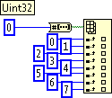
Is there a clever way to split a Uint32 in 32 bit directly accessible (not a prison guard) in LabVIEW FPGA?
The only way I could come up with is the following, which is a writing of pain for 32 bit and seems a waste resources og to store all these clues.
.
Best regards, mola
I thought about it. I could use clusters by right-clicking on the table to the Cluster block and increase the cluster size in 32.
Tags: NI Software
Similar Questions
-
LabVIEW FPGA: Integration node clock wrong
Hello
I'm having some difficulties to understand how the clock is part of the node IP for LabVIEW FPGA and was hoping to get some advice.
What I try to do is to set up a digital logic circuit with a MUX feeding a parallel 8-bit shift register. I created the schema for this Xilinx ISE 12.4, put in place and can't seem to import the HDL code into an intellectual property node. When I run the VI, I am able to choose between the two entries for the MUX, load the output in the shift register, clearly the shift register and activate the CE.
My problem is that when I switch to the entrance of THIS, he should start 1 sec shift (Boolean true, SCR, High, what-have-you) in the registry once each clock period. Unfortunately, it instantly makes all 8 bits 1 s. I suspect it's a question of clock and here are some of the things I've tried:
-Specify the input clock while going through the process of configuring IP nodes.
-Adding an FPGA clock Constant as the timed loop.
-Remove the timed loop and just specifying the clock input (I'm not able to run the VI that I get an error that calls for a timed loop)
-Do not specify the clock to enter the Configuration of the IP node and wiring of the FPGA clock Constant to the clock input (I can't because the entry is generated as a Boolean).
-Remove an earlier version of the EC who had two entries up to a door and at ISE.
-Specify the CE in the process Configuration of the IP nodes.
-Not specify this in the process of setting up nodes IP and wiring it sperately.
-Various reconfigurations of the same thing that I don't remember.
I think I'm doing something wrong with the clock, and that's the problem I have. Previously, when I asked questions to the Board of Directors on the importation of ISE code in LabVIEW FPGA, a clock signal is not necessary and they advised me to just use a timed loop. Now, I need to use it but am unable to find an explanation online, as it is a node of intellectual property.
Any advice would be greatly appreciated, I'm working on a project that will require an understanding how to operate clocks the crux of intellectual property.
Thanks in advance,
Yusif Nurizade
P.S. I have attached my schematic ISE and the LabVIEW project with one of the incarnations of the VI. The site allow me to add as an attachment .vhd file, but if it would help I could just paste the body of the code VDHL so just let me know.
Hello Françoise,.
I spoke to the engineer OR this topic and it seems that it was sufficient to verify that your code works, by putting a wait function of 500 ms on the while loop to check that the registers responsible and clear. I'm glad that it worked very well!
-
LabVIEW FPGA: Problem compiling look-up Table
Current versions of software:
LabVIEW 2014 SP1
LabVIEW FPGA 2014
Xilinx Vivado
I'm having a huge problem in trying to compile my LabVIEW FPGA code.
Some recall of the code:
It's all in a SCTL.
I am streaming in a FIFO DMA and comparing it with the values previously stored in the shift registers (which are initialized to 0 at the start of the loop) in the SCTL.
The results of the comparison are then piled into a U16 and loaded into a lookup table (I use the LUT - 1 d), and I'm so help this LUT to decide what value will be charged to travel to record for the next iteration of the loop, which, in any case, would be either the current values of the flow, or the post previous registry value.
(It's a triage loop)
I am able to run very well in simulation mode code, but when I try to compile, I get this error:
"The selected object has a built-in shift register that makes the output on a particular loop iteration correspond to the entries in the previous iteration."
Connect the outputs of the object directly to a minimum number of nodes of Feedback or uninitialized shift registers. You cannot connect the outputs to another object.
See using LabVIEW for more information on the objects with registers embedded offset. »
Someone at - it ideas why this happens, and what might be the possible solutions?
I'm tempted to break it down into separate loops, but I prefer not to because it is now a loop (and working in my simulation).
I found my problem.
Any time that a LUT is in a chain shift register, it cannot:
1. be part of a string of shift register that has a variable initialized
2. follow-up to no decisive structure, like a box structure.
I just moved the position of LUT and it works.
-
Compilation of the variable results in LabVIEW FPGA
Hello. I would ask why LabVIEW FPGA generates different results of compilation for the same code. When I compile several times my code, the maximum speed and total changes bitfile slices generated according to the compilation, but I does not alter with the FPGA VI. In addition, is the precise relationship of compilation? Thank you
It's normal. The FPGA compiler starts to place pieces of code on the FPGA somewhat randomly and adjusts them until either the design adapts and responds to the criteria of the moment or there that the compiler determines that it cannot fit all the code and meet time constraints. The outputs that the FPGA VI generates when run will always be the same.
-
Model a block synchronous dual-port RAM with LabVIEW FPGA
This question caught my attention recently.
I am trying to model a particular design element called "RAMB4_S8_S8" with the LabVIEW FPGA module. This element is a block synchronous dual-port RAM allowing simultaneous access to two ports independently from each other. That being said, a port can perform read/write operation to this RAM while at the same time, the other port might be able to do the same thing. There are two opportunities of possible port conflict, however. The first is when both ports are trying to write to the same memory cell. The other scenario is when a port writes in a cell memory while at the same time the other port reads from it. Other than that, everything should be a legitimate operation.
In order to reproduce this I select memory block that is integrated into my FPGA target. An interface is configured to be the playback mode, and the other is set to write fashion. For the option of arbitration, I let the two interfaces to be "arbitrate if several applicants only. Then I got a compiler error when I tried to run my FPGA code for this model in a SCTL. The error message is something like "several objects to request access to a resource through a resource configured with option interface" arbitrate if several applicants only ", which is supported only in the single-cycle Timed loop if there is only a single applicant by interface.
This error goes away if I replace the SCTL with a simple while loop, but not what I would like to implement. So I wonder if there is a better solution to this problem, or is it just the limitation of the LabVIEW FPGA module.
Thank you.
Yes, you can use a form of conduct to perform the operations you want in the generations clock cycles, but all the code is inside a single SCTL. Basically, read the first address and storing in a register in a single cycle and then read the second address in the second clock cycle. This would allow you to two readings of valid memory every clock cycle 2. I have included a crude extract to illustrate the concept. The case selectors are identical with address A being connected to the memory in the true case, B in the case of fake address. Your biggest model memory dual port will be intact, but it will operate at 1/2 rate.
Take a look at the white paper that provides more details on the construction of memory:
Data on a target FPGAS (FPGA Module)
The ball on the memory block indicates that memory block double port cannot be applied in a configuration of reading, which is a double ROM. access read/write port must be imitated with custom code.
-
HELP - FPGA SPARTAN 3E-100 CP132 WORKS WITH LABVIEW FPGA?
HI EVERYONE, GET ON IM TRYING TO USE MY FPGA WITH LABVIEW, BUT I DO KNOW THAT IF ITS COMPATIBLE, I INSTALLED THE DRIVERS, MODULE FPGA AND LABVIEW 2012, IM USING WINDOWS 7 32 BIT, AND AFTER I COMPILED ITS SAYS:
LabVIEW FPGA called another software component, and the component returned the following error:
Error code:-310601
NOR-COBS: Impossible to detect the communication cable.
Check the communication cable is plugged into your computer and your target. Also, verify that the proper drivers are installed.Thank you.
=)
Hi dvaldez2.
LabVIEW FPGA offers no support for any material to third parties, other than the 3rd Spartan XUP Starter Kit. These are probably the drivers you downloaded.
http://digital.NI.com/express.nsf/bycode/Spartan3E?OpenDocument&lang=en&node=seminar_US
However, this driver supports only the Starter Kit Board itself (http://www.digilentinc.com/Products/Detail.cfm?NavPath=2, 400, 790 & Prod = S3EBOARD). You may not use the driver with any other Xilinx FPGAS.
I hope this helps.
-
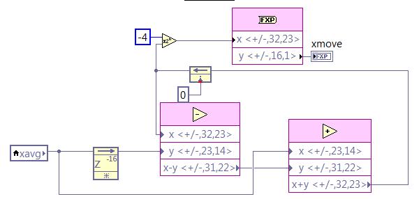
I created a Labview FPGA .vi using a structure flat sequence that shows the output of a sensor at a sampling frequency of 1 kHz on a digital SPI. After reading, I write the point data fixed in a FIFO, which is read by a host vi and finally written on the hard disk for post-processing. I need to add logic for the calculation of the average for the further process the signal FPGA vi. I want to continue at the exit of the original 1 kHz sampled datat to the FIFO, but also perform a sprawl on the steps and write these results at the same frequency of 1 kHz to the FIFO. The average feature, I would like to implement is a two-step process. Step 1 is to take samples of 1 kHz and perform an average of 16 samples based frame. In other words, I want samples of sum 16 1 kHz and dividing by 16 and decimate 16:1, which produces data of 62.5 Hz. Step 2 is to take 62.5 Hz sampled data and perform a moving average of 16 samples on these data and output resulting at the same sample rate of 62.5 Hz. I want these 62.5 Hz sampled data to be injected into the FIFA as well as the original data of 1 kHz sampled (unmodified) at the frequency of 1 kHz.
I've got step 1 work correctly using the block "mean, Variance, StdDev FPGA vi" with number of samples on 16. This block runs within a sequence of flat sequence structure after I received each sample 1 kHz on the SPI. My fight is the average feature mobile step 2. I try to use the code in the screenshot below, but am unclear regarding how/where to implement this logic inside is my structure flat separate sequence while loop, structure of the case, etc, in order to ensure that it only works on one of 62.5 Hz samples to this flow of data at once. I tried to put it inside the sequence that executes the block average and further in a case that is driven by the Boolean "valid" the average block output. I obviously don't understand how these different loops run, because it does not work properly. Can someone tell me how to implement the logic of moving average in my vi FPGA existing to produce the desired results as described above? Screenshot below of the logic (step 2) average mobile I am trying to use. In addition, find attached my screws vi FPGA that I need help with is 'CA215_SPI.vi' and the level vi host is 'Host.vi '. Thanks in advance.
Joel
This question is closed. I realized that my approach to implementation was actually working. I just had a stupid mistake on my fixed point output bit size, giving me results errenous.
-
CPU register accessible in LabView FPGA FlexRIO
Hello people, I wonder if it is possible to get the following behaviors of Labview. I think that it is not.
Description of the system: application of CVI which communicates with SMU FlexRIO via controls and indicators.
Problem: The design of a CPU-FPGA interface specification which lists the "books" as a combination of reading and reading/writing-the bit fields.
Example:
According to the specification, there should be a 32-bit register. 31: 16 bits are read-only, and 15:0 bits are read/write, from the perspective of the CPU. In the world of labview, I would just do a uint16 control and indicator of uint16 and do with it.
However, to meet the specification (written for microprocessor buses) traditional, a reading of 32 bits of an address should read back the full content of the 32-bitregister to this place (implemented as flops on the FPGA, with appropriate memory within the FPGA device mapping). In the same way a 32 bits of an address entry must store the values in this registry (properly masking wrote at 31: 16 bits within the FPGA device).
Is it possible for me to have a unique address (basically, a component unique labview block diagram) that will allow me to accomplish this behavior? It seems to me that the only solution is to pack my records with bit fields that are all read, or all the read-write in order to register in the paradigm of labview. This means that the spec should go back and be re-written and approved again.
Thanks in advance,
-J
Thanks for the detailed explanation. I am familiar with the reading and writing in the FPGA registers - I did a lot of work non-LabVIEW recently with an Altera FPGA. I haven't, however, used the CVI to LabVIEW FPGA interface, I only used the LabVIEW interface. I'm not sure if your question is about the CVI, LabVIEW FPGA interface or both.
JJMontante wrote:
Thus, a restatement of my original question: y at - it a mechanism with the use of indicators of controls where both the FPGA AND the CPU can write to the same series of flip-flops in the FPGA? If I use an indicator, the FPGA can write to the indicator, but the CPU cannot. If I use a control, the CPU can write in the control, but can't the FPGA. Is this correct?
On LabVIEW FPGA, a control and indicator are essentially identical. You can write a check, or read a battery / battery, using a local variable in the FPGA code. It is common to use a single piece of front panel to transfer the data in either sense, and it's okay if it's a command or an indicator. For example, a common strategy uses a Boolean façade element for handshake. The CPU writes a value to a numeric control, and then sets the value Boolean true to indicate that the new data is available. FPGA reads this numerical value, and then sets the Boolean false, which indicates the processor that the value has been read. The LabVIEW FPGA interface (side CPU) covers also all elements of frontage on the same FPGA whether orders or the lights--they can be as well read and written.
That answer your question at all?
-
Question for LabVIEW FPGA DRAM
Hi all
How can I correctly address the 128 - bit DRAM memory? I have the Bank DRAM 0 set as a memory of 128 bits, set up in my design as a CLIP. I realize it's a wide RAM on 32-bit. I had a National Instruments AE do the original design I've been adding to. He said that the addresses needed to incrementing by four with each entry. Example: if I had to write in consecutive addresses, I would write to the address: 0, 3, 7, 11, 15 etc, and I would like to send 128 bits to each address. My address is calculated as: (number of pixels in a line of video + line * (number of pixels per line) for a picture of the video). So I take my calculated address and add 4.
However, I checked an example in the finder example: example of integrity hardware flexRIO/IO/external memory/memory. In this example, 128-bit data is sent to the memory and the address is incremented by 1 (instead of 4) each cycle clock as valid data.
Who is this? Section of the help for this function is ambiguous.
Sets the address in external memory for reading or writing. The physical data bus for external memory is 32 bits wide (4 bytes). Each unique address value represents 4 bytes of data. Therefore, the total number of unique addresses in external memory is equal to (Memory Size in bytes)/4.

Note  The memory interface exposed to LabVIEW FPGA is 128 bits wide. As a result, each memory write or read operation accesses four different address locations in memory. The memory controller latches this signal value only when you issue a new memory write command by asserting the Command_Write_Enable signal.
I'm confused by the 2nd paragraph "every Scripture memory or read operation four access address locations of memory." Does that mean I increment the address by 1 to get 128 consecutive bits 'locations' (Yes, I know, that's 4 words of 32 bits in memory), or do I increment the address by 4, in the order of words of 32 bits 4 by 128-bit single transfer?
Thanks for your help.
-J
Hello J,
I want to clarify my previous post. There are two ways to access memory DRAM, CLIP (that you have described is what you do) and using the memory node. As noted before, the DRAM is 128 bits wide. When you write to the CLIP you basically write pieces that is the width of the databus (in this case 32-bit). Therefore, when you write a total of 128-bit DRAM, you place 32 bits in each address. The address being the width of the databus, then you write with a writing & the address 0, 1, 2, 3. Then the next write will be 4, 5, 6, & 7 and then address 8, 9, 10, & 11 and so on. In this case, you must increment your address by 4 whenever you write. Note that you start at 0, then 4, then 8, etc 12. In your previous post, you were out of a figure.
There is also another way to write in the DRAM memory, and it is through the node of memory, which is what is used in the example that you are pointing out. Here, LabVIEW takes on some of the thought, and instead of being the width of the databus address, they are the width of the entire segment of 128 bits. So when you write to DRAM here, you only increment 1 whenever address because they refer to any segment of memory. This contrast with the CLIP, address 0 of the memory node interface match the addresses 0, 1, 2, 3 in CLIP mode & and address 1 of the memory node would correspond to 4, 5, 6, 7 in CLIP mode addresses &. If you do not write an integer of 128 bits for the memory node, then the remaining addresses in the data block are filled with "junk" so that the address remains constant.
As I mentioned previously, it is the most effective writing in chucks of 128 bits so that you don't waste all of the DRAM. I hope you find this explanation clearer.
Brandon Treece
Technical sales engineer
National Instruments
-
Need for SOUL of breaking into pieces of 4 GB.
I send a video clip of 25 minutes 1080p24fps via a CF card in the editor. Would be nice if SOUL had an option to do this. If so, I don't know. Looks like my only option is to break the sequence in small sequences myself and export them separately.
True?
Next time I'll ask for a disk instead of a card CD external HARD...
I don't think that the SOUL has that capability directly. I will be corrected, if wrong.
Instead, just use the WAB (work area bar) to export in the pieces that you need. Since you're dealing with file sizes and no duration, a little bit of math will be required.
Another possibility would be to use an archiving program like WinRAR to split the file into pieces to your specifications. The recipient should then the program to "mount" the files on their computer.
Another option would be to ship on a drive external HARD, rather than on a map. Packaging and shipping costs will increase slightly, but this is how to send large files and usually have a couple of external transit at any time.
Good luck
Hunt
-
Why do I get texts into pieces and in the mess of others?
Why my iPhone OS 6 more 9.2.1 receive texts into pieces and out of use? Of it only happens with only the texts of some people, not everyone else.
If it's TEXT and not iMessage (green bubble) then it is a function of carrier. Different companies have their "gateways" configured differently and so long texts can sometimes be break. Are the cases where this happens - individuals with one carrier other than yours?
-
Simulate the sine wave using LabVIEW FPGA with NOR-myRIO and display in real time
Hello
I'm relatively new to LabVIEW FPGA. I am trying to test (and later apply) controllers high speed on myRIO.
At this point, I'm trying to simulate the sine wave from 1 to 10 kHz using Sinewave generator VI express. I also intend to display the sine wave on the time real (RT) using FIFO. However, I had a bit of trouble to understaing various synchronization parameters.
1. how to encode information about the sampling frequency generating sine wave? (The side FPGA vi requires only the frequency of the signal and possibly phase and does not rate update lines)
2. how to estimate the number of items in a FIFO? (that is, the relationship between the rate of updates to loop (RT), the signal frequency, sampling frequency and the number of items in the FIFO)
It would be great if we could share a very simple program (side host and target) that did something similar.
Thank you
MILIN
Milot,
I think the problem is the type of data in your FIFO. Your FIFO is configured to use a data type of I16. The problem is the number, it displays only ever will be-1, 0 or 1. To resolve this problem, you must send the sine wave as a fixed point data and convert it to a double on the side of the RT. This should significantly improve your resolution.
-
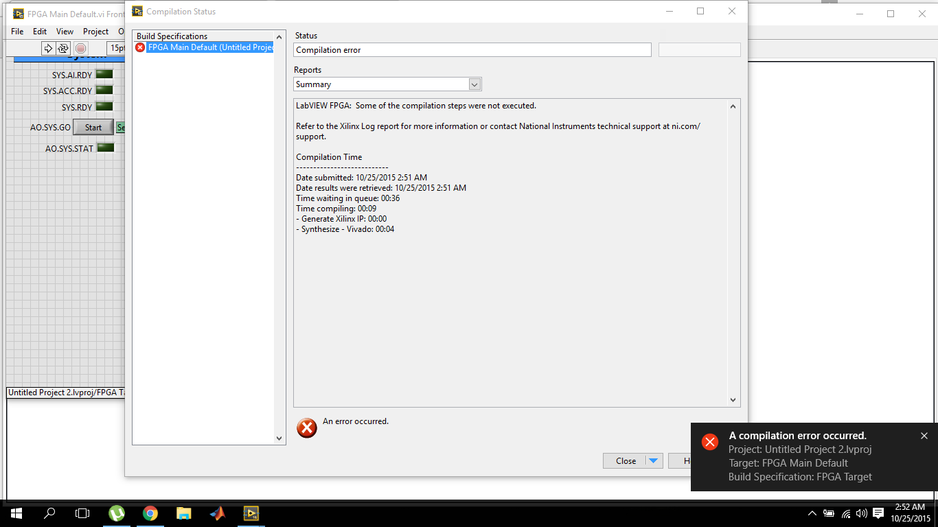
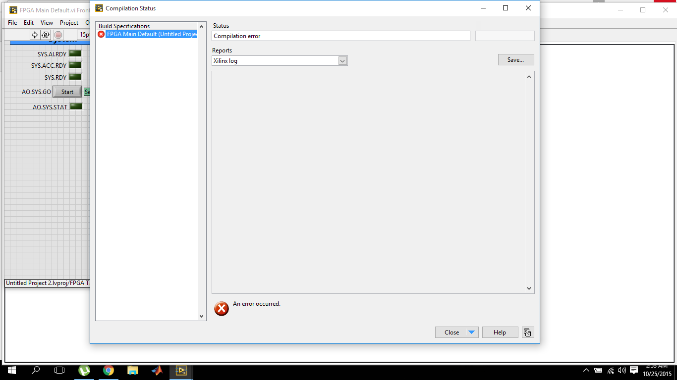
LabVIEW FPGA, 2015 compilation error
I've recently switched to LabVIEW 2015 and I'm working on OR myRIO. So also installed myRIO 2015 bundled software. The problem I have is that the compilation of fpga fails within 10 seconds.
and the target Xilinx journal report is empty
The first time when I tried to compile on 2015 version, it failed and the message box that failed came alongwith the avast antivirus warning for malicious activity. I reported it as wrong and now I tried several times with avast shield disabled control, but the results are the same. While the version of labVIEW 2014 works very well.
Now, I'm sure that there is something wrong with the installation of Vivado because this dll is part of it. The dll must be default in the2014_4\lib\win32.o directory C:\NIFPGA\programs\Vivado if you are using an operating system for 32-bit AND also in C:\NIFPGA\programs\Vivado2014_4\lib\win64.o If you use a 64-bit operating system. If the dll is not here, it is probably that the anti virus (I've never seen what happens to Xilinx but I have for other stuff).
I'm emphasizing the 2014_4 because LabVIEW 2015 uses Vivado 2014_4 while 2014 LabVIEW uses Vivado 2013_4. Since you have also installed LabVIEW 2014, you must have 2013_4 as well and if it works, you will find the dll I just wanted you make sure you check the correct directory for the Vivado 2014_4.
Download and install (reinstall or repair if already installed) 2015 LabVIEW FPGA Module Xilinx tools Vivado 2014.4. You can also use the DVD Setup if you have. It would be a good idea to do the installation with the disabled and even anti-virus try the first compilation the same. Try and let me know if the problem persists.
Kind regards
-
Internal software error of LabVIEW FPGA Module - 61499
I get the error next (in a pop-up window) in the phase of sompilation for the FPGA target with a vhdl IP. This error continues to occur even after restart LabVIEW and the PC. Someone at - it solved is this kind of problem before without having to re - install the software?
Here is the error information:
Error-61499 occurred at niFpgaXml_GetValue_String.vi<><><><>
Possible reasons:
LabVIEW FPGA: An internal software error in the LabVIEW FPGA Module has occurred. Please contact National Instruments technical support on ni.com/support.
Additional information: lack the tag required XML (/ CompileServerList)
As a first step, I can compile the vhdl IP node successfully. However, once when I'm running a VI with the FPGA, the bureau stop working. After that I restarted by force, it cannot perform the build of a vhdl IP node. Even without connecing to the jury of LabView, he pointed out errors before the end of the sompilation.
Interestingly, the screw which also includes nodes IP vhdl that I properly compiled before, I can still run the VI to the Commission and it works correctly.
Thank you
Looks like your ActiveJobsList somehow has been corrupted. I saw occur when computers are hard stop or blue screen during compilation. I don't have that LabVIEW 2014 installed on my machine, so your path will be a little different, and the file extension will be a .txt or .xml instead of .json, but try this:
Move the file "C:\Program Files (x 86) \National Instruments\LabVIEW 2014\vi.lib\rvi\CDR\niFpgaActiveJobList.json" (or your equivalent) out of the above directory (back it upward and delete essentially) and restart LabVIEW. Must regenerate the file and resolve the problem.
-
How to use bidirectional I/O in the CLIP of LabVIEW FPGA?
How to use or define two-way i/o for CLIP with LabVIEW FPGA? I want to use 1-wire communication inside the kernel CLIP, the function will be implemented to read and write as I/O inside the CLAMP.
The XML Generator (CXG) 1.1.0 ELEMENT does not support.
Thank you
Supawat
Work after separate IB pin (bidirectional) at the entrance and exit. Thank you.
Maybe you are looking for
-
Hello My iphone4s did not reverse through wifi so I thought to do factory restore, when I restored via itunes updated firmware has failed, I tried 20 times same question, service center, I went and told that your camera has not, exchange of he's with
-
Downloaded the new version 8.1, but don't 'applies' said is not sufficient previledges?
After having downloaded the new firefox version 8.1 could not follow the 2 steps. When Fox drag the application icon when prompted click on replace existing version, but guest said he can't do it because I do not have sufficient previledges. How can
-
Problems of updating BIOS on Satellite L40 - 15G
Good afternoon. I have Toshiba Satellite L40 - 15G and I want to put 4 GB of ram (2 x 2).It works with 3 GB but with 4 GB it just does not start - gives me a blue screen. I read on the internet and discovered that I have to update my BIOS (my version
-
How to enable IR on the Satellite A500/031
Does anyone know how to activate the IR port of a Toshiba A500/031 (part - PSAR9A-031001 number)? I can't find how to turn it on.
-
SL500 and I want to add more RAM
Howdy. I have a new Thinkpad SL500, such as here: http://www.hemini.com/products/product_details.aspx?prodid=425737&cp=1&sc=1&sct= It has an Intel Core 2 Duo (T6670) 2.2 GHz processor and 2048 MB of RAM. I want to add more RAM to make it even more ef