Nominal voltage setting?
Hello
I want to connect a sensor piezoresistif (strain gage bridge) directly to my USB - 6216 BNC. I know that this device is not a source of internal excitement so I'll have to provide myself. So I think that the best thing to do then, is measure the output voltage of the sensor with one of the analog inputs. The output voltage of the sensor full scale is 300mV +/-100 mV, but for our purposes the working range is less than 200 mV. Page 5 of the specifications for the USB-6216, I have found that the sensitivity is 5.2 µV if the nominal range is between 0, 2V and - 0, 2V. Now my question is how to do, I put this voltage? I use the Signal Express 2012 but I'm a bit confused. If I add a step and choose "DAQmx Axquire"-> "Analog input"-> "Power" then I am able to choose 'Signal Input Range. This is how the nominal voltage is determined?
The sensor also has a very high frequency response if I want to make some measurements at the maximum rate of the device (400 kHz). We don't expect high-frequency signals, but it's something that we want to check. At the appliance a few built-in anti-aliasing or filtering?
You set the range. That defines the sensitivity of data acquisition. In your case, set it to 0.2.
As far as the frequency is concerned, DAQ served only at 400kS/s. Which means that you can't really capture any signal above 200 kHz (Nyquist).
Tags: NI Hardware
Similar Questions
-
How to find or change the voltage setting set in a series of HP TouchSmart IQ500
How do I find or change the voltage setting set in a series of HP TouchSmart IQ500 (specifically an IQ524)
It does not use an external power adapter? If so, all you need to use in another country is an adpater sheet to match the wall outlet.
-
Measure the voltage of strain gauge
I have connected my 9237 to a 9945. I use a 350 ohm strain gauge. I have the voltage set to 2, 5V Max is there a way to measure physically to be sure that it is 2.5V? Also, in my vi I use a DAQmx create function of the channel. I want to add another channel for this but can't see how to do it.
Thank you
HS
Hi, Harry, it's Paul with engineering Applications to the OR.
My first question is why you are wanting to physically measure the voltage?
If you are wondering how that tension may vary, it is limited by the maximum capacity of 150mW of your device, as explained here: http://digital.ni.com/public.nsf/allkb/7CBC67482CC9FB318625758C0048FF73?OpenDocument
If you want to continue to measure externally, you have a few options. You can use another DAQ hardware to measure the voltage, or you can use another external device, like a digital multimeter.
If you want to see in the excitement that is actually supplied LabVIEW code, you can use the node property DAQmx 'Value of real excitement'.
As far as playback of multiple channels, theres two ways you can go about it. If your channels are sequential and all have the same settings, then you can change your name of the physical channel to something like 'Dev1/ai0' to ' Dev1 / ai0:3: to specify the first 4 channels.» Alternatively, if you wanted to select non sequential channels, you can chain create channel set tasks, as long as they are of the same type of task (AI voltage, etc.) and the same device, as shown below.
Let us know if you have any other questions.
Kind regards
Paul
-
Hi all
I am currently using Agilent E3646A dual output DC power supply.
I'm sweeping the 2 output voltages by using 2 loops, 1 inside the other.
The attachment shows the connection that I have.
However, only the inside of the loop works. The outer loop, seems to work on the Panel before labview, but it does not change the nominal voltage of E3646A.
Any help? Or is there a connection error? I'm new to labview.
Thank you very much!
Dear Daniel,
Thanks for your suggestion.
I moved drivers in loops, leaving the initialization and the error/close to the outside, and it works.
Thank you much for the help

See you soon
-
Generation of voltage USB-6501
Hi all
I am very new to the use of devices to LabView and NI, so forgive me if my question seems stupid.
I have an acquisition of data NI USB-6501 I want to use to connect to a device that will open or close a lid when triggered.
My question is: is it possible to programmatically trigger the nominal voltage of the USB-6501?
I'm using LabView for this and I am running on Windows 7. I couldn't find examples of LabView bases that were related to the output voltage for the USB-6501.
Any help would be really appreciated, thanks in advance
Thanks for your replies.
After a few changes, the example "Write dig Chan" helped me to get the behavior I want to put on and a device plugged power off.
-
Agilent U2722A linear voltage ramp
I am currently writing a LABVIEW VI to interface with an Agilent U2722A. I want to measure current constantly while maximum increase of voltage of 0V to a defined use specifying the step size and no time (a linear scan of tension).
I downloaded the driver for this device which also includes an example used for output and then take action. My first problem is that when I run this unit VI is to expire. I think that this issue MAY have something to do with the entry "triggered the level". Happened to configure voltage channel VI. I have included the example and the voltage setting channel Sub VI.
My lack of understanding for the other SubVIs (which are based on being passed SCPI commands by VISA as strings) also prevents me from making progress. Especially the scan configures and configure trigger screws
Scanner Confgiure takes the values for the number of points and the timestep. I don't know how I'm supposed to make use of this VI. Should I put the values you want, and then use a loop to pass different values to the chain tension set up with each iteration. Also, how is the measured timestep? I need to set up a trigger to measure the time between the points or the scan function takes care of that? I've included the sweep set up VI as the Timestep VI as well.
Looks like that you've got another error in connection with the IO instrument. Here are some references for this error,
-420, "request not COMPLETED;
This error occurs when you addess the instrument to talk and he has nothing to say.
The most likely causes are:
1. do not send a query. You must send a valid request to the instrument before talking to talk to him. This is true even of the instruments of measurement, such as the 2001 model. You can not get a reading from 2001 until you send him a request.
2 send an invalid request. If you sent a request and still get this error, make sure that the instrument treats the query without error. For example, send a bad request that generates an error - 113, "Undefined header" and then treat the instrument to speak will generate an error-420, "Request not COMPLETED" as well.
3 query invalid due to an invalid command.
Currently I do not have an instrumetn in hand so I can't understand what is exactly what's wrong, but would you mind to paste your code so that we can look into it together?
The most accurate method is absolutely one provided by the material itself. Here is "Interval" in configure Sweep.vi.
-
Question about multi analog outputs voltage outfit
I am programming my NI USB-6008 with V ++.
Now, I have a question. The unit has 2 analog outputs.
When I put the "ao0" channel to a certain tension, then stop this task. Start another task, then the string value "ao1" some tension. When I do the second task, ao0 held the voltage set in the first task?
Thank you.
Hi Lowsfer-
Yes, the analog output of AO1 status will remain in the last State it was before the task is stopped. As long as the device is not reset or the computer is not turned off, the analogue output will maintain the last tension that you specified, regardless of what did the other Ao channel.
I hope this helps. Good luck with your application!
-
'voltage design' vs real 'tension' in the power manager
Just today, all around the navigation in the power manager, I noticed that the values of 'design' and 'tension' on the 'battery' tab are different! The "design power" reads 11.10V, while the 'tension' reads 12.06V.
I feel that it is actually normal... but maybe someone can confirm my suspicions? Out of curiosity, why these two values differ and what that means?
I use using a T510 running on win7 x 64, if this is no help at all.
voltage will drop over time, while the nominal voltage provides a constant reference point to tell you what kind of condition is in your battery, and if it needs to be replaced.
-
Hello
I want to add some extra memory to my machine, but I want to make sure that I get the memory with the same nominal voltage for maximum compatibility.
The machine is a HP Pavilion HPE H8-1070uk
Product number: LN874EA #ABU
Model: H8-1070uk
HP admits not knowing the answer, which is a little disturbing considering his equipment!
Anyone have any ideas?
See you soon.
I suspect the most common voltage for the memory of your system is 1.5volts, but to be sure, click the link below for CPU - Z;
http://www.cpuid.com/downloads/CPU-z/1.58-Setup-en.exe
and run this program to determine the operating voltage of the currently installed memory. Go to the tab labeled 'SPD' to find the specifications you are looking for. This should include the type, speed and voltage.
Frank
-
Satellite L500-22R - memory problem
I tried to upgrade my Toshiba L500-22R memory up to 8 GB. I bought 2 x 4 GB Kingston SODIMM 12800 PC3L, the operating system does not start, I did a check of memory and it fails too. I tried with a Samsung 4 GB 12800 and it fails too.
The original memory works well.
Any ideas?
TXT of CPU - Z report:
CPU - Z version 1.72.0.x64Information for processors
-
Processor 1 ID = 0
Number of cores 2 (max 8)
Number of threads 4 (max. 16)
Name Intel Core i5 430M
Code-named Arrandale
Specification Intel (r) Core i5 CPU M 430 2.27 GHz
Package (platform ID) Socket 989 rPGA (0x4)
CPUID 6.5.2
CPUID long 6.25
Core Stepping C2
The 32nm process technology
TDP limit 25.0 Watts
Basic speed 1187,2 MHz
Multiplier x Bus 9.0 x 131.9 MHz speed
2374,3 MHz rated Bus speed
Stock frequency 2266 MHz
Instructions sets MMX, SSE, SSE2, SSE3, SSSE3, SSE4.1, SSE4.2, EM64T
Data L1 cache 2 x 32 KB, size 8-way line set associative, 64 bytes
L1 instruction cache 2 x 32 KB, size 4-way set associative line, 64 bytes
L2 cache 2 x 256 KB, size 8-way line set associative, 64 bytes
Cache 3 MB L3, size 12 channels line set associative, 64 bytes
FID/VID control YesChipset
-
Northbridge Intel Havendale/Clarkdale Host Bridge Rev 02
Southbridge Intel HM55 Rev. 05
Graphics interface PCI-Express
Width link PCI-E x 16
PCI-E Max Link width x 16
Type of DDR3 memory
Memory size 4 GB
Double channels (symmetrical)
Memory frequency 527,6 MHz (04:16)
Latency CASE # (CL) 7.0
RAS # for CASE # delay (tRCD) 7
RAS # Precharge (tRP) 7
Cycle Time (tRAS) 20
Time to Row Refresh Cycle (tRFC) 60
Control rate (CR) 1 t
Base address e/s MCHBAR 0x0FED10000
E/s MCHBAR size 4096Memory SPD
-
DIMM # 1
SMBus address 0 x 50
Type of DDR3 memory
Format of SO-DIMM
Manufacturer (ID) Samsung (CE000000000000000000)
Size 2048 MB
Bandwidth Max PC3-8500F (533 MHz)
M471B5673FH0-CF8 part number
Serial number 62B15B6F
Date 12/year, 10 weeks of manufacturing
Number of banks 8
Nominal voltage 1.50 Volts
EPP no
XMP no
AMP noDIMM # 2
SMBus address 0 x 52
Type of DDR3 memory
Format of SO-DIMM
Manufacturer (ID) Samsung (CE000000000000000000)
Size 2048 MB
Bandwidth Max PC3-8500F (533 MHz)
M471B5673FH0-CF8 part number
Serial number 62B15B87
Date 12/year, 10 weeks of manufacturing
Number of banks 8
Nominal voltage 1.50 Volts
EPP no
XMP no
AMP noModel of card mother NSWAA (0x0000017A - 0 x 00035690)
DMI
-DMI BIOS
seller TOSHIBA
version 2.10
day 05/17/11
ROM size 2048 KBSystem DMI information
Manufacturer TOSHIBA
product Satellite L500
version PSLS9E-02Q01TCE
series 3A747581K
UUID {9ED22C15-2032-DF11-B751-705AB6880D1F}DMI Baseboard
seller TOSHIBA
model NSWAA
Revision 1.00
series 123456789ABOf course, you bought not compatible modules.
PC3 12800 1600 Mhz isn't listed as a module support.Satellite L500 can scale up to 8 GB of RAM and you can use two modules MHz (PC3-8500) 4 GB DDR3 SO-DIMM 1066.
-
My memory works ok? (Additional JEDEC listed)
Additional JEDEC #6?
I bought this 2 GB of http://tinyurl.com/2urvxgl key to upgrade my laptop to 4 GB. Because I mix I wanted to make sure that all manufacturers (Micron & Samsung) is very well by running CPUz diagnostics and noticed that Micron module has an additional entry in the JEDEC timing Table (it lists JEDEC #6 10.0 - 10-10-28-38 761 MHz) I also noticed the Micron stick seems to have a different number of chips on the stick of RAM too compared to the Samsung RAM.
-Is this normal? -Do you think I'm getting double channel of this mix of manufacturers?
I guess the worst case scenario is to order another Micron 2 GB stick so that I have identical, but all pairs seems OK so far.
Model of laptop: HP G62-a15SAPlease see below for info extracted by CPUz memory:
Chipset
-------------------------------------------------------------------------
Northbridge AMD 785GX Rev. 00
AMD Rev SB800 southbridge. 40
Type of DDR3 memory
Memory size 4096 MB
Double channels, (Unganged)
Frequency 532,5 MHz (3:8) memory
Latency CASE # (CL) 7.0
RAS # for CASE # delay (tRCD) 7
RAS # Precharge (tRP) 7
Cycle Time (tRAS) 20
Cycle time of Bank (tRC) 27
Control rate (CR) 1 t
Uncore frequency 1597,4 MHz
Memory SPD
-------------------------------------------------------------------------
DIMM # 1
SMBus address 0 x 50
Type of DDR3 memory
Format of SO-DIMM
Manufacturer (ID) Micron (2 00000000000000) Technology
Size 2048 MB
Bandwidth Max PC3-10700 (667 MHz)
Part number 8JSF25664HZ-1G4D1
Serial number 3116004D
Date 29/year, 10 weeks of manufacturing
Number of banks 8
Nominal voltage 1.50 Volts
EPP no
XMP no
Timings JEDEC CL-tRCD-tRP-tRAS-tRC table @ frequency
JEDEC #1 5.0 - 5-5-14-19 @ 380 MHz
JEDEC #2 6.0 - 6-6-17-23 @ 457 MHz
JEDEC #3 7, 0-7-7-20-27 @ 533 MHz
JEDEC #4 8, 0-8-8-22-30 MHz 609
JEDEC #5 9.0 - 9-9-25-34 @ 685 MHz
JEDEC #6 10.0 - 10-10-28-38 761 MHzDIMM # 2
SMBus address 0 x 51
Type of DDR3 memory
Format of SO-DIMM
Manufacturer (ID) Samsung (CE00000000000000)
Size 2048 MB
Bandwidth Max PC3-10700 (667 MHz)
M471B5673FH0-CH9 part number
Serial number 78FDDF59
Date 14/year, 10 weeks of manufacturing
Number of banks 8
Nominal voltage 1.50 Volts
EPP no
XMP no
Timings JEDEC CL-tRCD-tRP-tRAS-tRC table @ frequency
JEDEC #1 5.0 - 5-5-14-19 @ 380 MHz
JEDEC #2 6.0 - 6-6-17-23 @ 457 MHz
JEDEC #3 7, 0-7-7-20-27 @ 533 MHz
JEDEC #4 8, 0-8-8-22-30 MHz 609
JEDEC #5 9.0 - 9-9-25-34 @ 685 MHzStudio_Muppet wrote:
Hi erico!
I thank you for your reply, noted that the SPD does not give abilities - having a JEDEC extra listed on my new stick of RAM and not the other question? It does not matter. Those are the timings primary, secondary and tension that a BIOS can use to automatically set the memory at FSB speeds.
Also, I noticed a change in the frequency of frequency & DRAM NB when comparing the original configuration of 3 GB for my new 4 GB configuration: old Vs new Config
Is this normal?
The speed of the memory takes by default the slowest speed. Consider yourself lucky that it starts in Windows. Most do not have that kind of luck and is frustrated to have the new memory that does not work in their notebooks.

Sorry for my lack of knowledge, I want to be sure I'm not compromising performance by mixing RAM from different manufacturers. If additional memory is slower than the original memory then you have slowed the operations of memory and essentially lost some performance. I see it running in dual channel. It's a surprise. Lucky you!

Best regards
ERICO
-
Need help upgrading my alienware aurora
Here are all the technical features of cpu - z, keeping in mind both the original production (HD5670x2 crossfire) doesn't have a video card, I currently installed I picked up to 49.99 (half price) I was looking in the privateer, unit cooling, but even under the huge load, my computer runs at 27 c so... I have 12 GB memory, I want to game time to load faster... can I switch the processor without having to tear the entire computer? Maybe just the PSU and CPU? the cpu is removable for a best i7? that would help? cause I'm sure that the 12 GB of memory is not in desperate need of good memory? IM xcom2 to play and wait a good 2-3 minutes between the levels on the loading time... Anyway here is the screenshots, and below that is the cpu - z text file

TXT of CPU - Z report
-------------------------------------------------------------------------Binary files
-------------------------------------------------------------------------CPU - Z version 1.76.0.x64
Processors
-------------------------------------------------------------------------Number of processors 1
Number of threads 8APICs
-------------------------------------------------------------------------Processor 0
-Core 0
-Wire 0 0
-Thread 1 1
-Core 1
-0-2 wire
-Wire 1 3
-Core 2
-0-4 wire
-Wire 5 1
-Core 3
-0-6 wire
-Wire 1 7Timers
-------------------------------------------------------------------------Timer ACPI 3,580 MHz
Timer HPET 14,318 MHz
Timer perf 2,741 MHz
Sys 1,000 KHz timerInformation for processors
-------------------------------------------------------------------------Processor 1 ID = 0
Number of hearts 4 (max 8)
The number of threads 8 (max 16)
Name Intel Core i7 930
Codename Bloomfield
Specification Intel (r) Core i7 CPU 930 @ 2.80GHz
Package (platform ID) Socket 1366 LGA (0 x 1)
CPUID 6.A.5
CPUID extended 6. 1A
Core Stepping D0
The 45 nm technology
TDP limit 130.0 Watts
Basic speed 2940,5 MHz
Multiplier x Bus 22,0 x 133,7 MHz speed
2405,9 MHz rated Bus speed
Stock frequency of 2800 MHz
Instructions sets MMX, SSE, SSE2, SSE3, SSSE3, SSE4.1, SSE4.2, EM64T, VT - x
Data L1 cache 4 x 32 KB, size 8-way line set associative, 64 bytes
L1 instruction cache 4 x 32 KB, size 4-way set associative line, 64 bytes
L2 cache 4 x 256 KB, size 8-way line set associative, 64 bytes
Cache 8 MB L3, size 16-way set associative line, 64 bytes
FID/VID control YesTurbo Mode supported, enabled
3066 MHz Max turbo frequency
Max-non-Turbo report 21 x
Max turbo report 23 x
Max efficiency report 12 x
TDC limited 110 amps
Number of bus max 255
PCI peripheral device connected to the 255 bus, device 2, function 0
PCI peripheral device connected to the 255 bus, device 3, function 4Temperature 0 57 ° C (134 ° F) [0x2B] (Core #0)
Power supply 0 40.52 W (package)Thread dumps
-------------------------------------------------------------------------CPU thread 0
APIC ID 0
Topology Processor ID 0, Core ID 0, Thread ID 0
Type 01020001:
0000000Bh Max CPUID level
Level of position Max CPUID 80000008 h
Descriptor level 1, D, 32 KB, 2 wire (s) cache
Descriptor level 1, I, 32 k, 2 wire (s) cache
Descriptor cache level 2, U, 256 KB, 2 wire (s)
Descriptor cache level 3, U, 8 MB, 16 threadsCPUID
0 x 00000000 0x0000000B 0x756E6547 0x6C65746E 0x49656E69
0 x 00000001 0x000106A5 0 x 03100800 0x0098E3BD 0xBFEBFBFF
0 x 00000002 0x55035A01 0x00F0B2E4 0 x 00000000 0x09CA212C
0 x 00000003 0x00000000 0x00000000 0x00000000 0x00000000
0 x 00000004 0x0000003F 0x01C0003F 0x1C004121 0x00000000
0 x 00000004 0x1C004122 0x00C0003F 0x0000007F 0x00000000
0 x 00000004 0x1C004143 0x01C0003F 0x000001FF 0x00000000
0 x 00000004 0x1C03C163 0x03C0003F 0x00001FFF 0x00000002
0x00000005 00000040 0 x 0 x 00000040 0 x 00000003 0 x 00001120
0 x 00000006 0 x 00000003 0x00000002 0x00000001 0x00000000
0 x 00000007 0x00000000 0x00000000 0x00000000 0x00000000
0x00000008 0x00000000 0x00000000 0x00000000 0x00000000
0 x 00000009 0x00000000 0x00000000 0x00000000 0x00000000
0x0000000A 0 x 07300403 0 x 00000044 0x00000000 0 x 00000603
0x0000000B 0x00000001 0x00000002 0x00000100 0 x 00000003
0x0000000B 0 x 00000004 0x00000008 0 x 00000201 0 x 00000003
0x80000000 0 x 80000008 0x00000000 0x00000000 0x00000000
0 x 80000001 0x00000000 0x00000000 0x00000001 0 x 28100800
0 x 80000002 0x65746E49 0x2952286C 0x726F4320 0x4D542865
0 x 80000003 0 x 37692029 0 x 55504320 20202020 0 x 0 x 20202020
0 x 80000004 0 x 30333920 0 x 20402020 0x30382E32 0x007A4847
0 x 80000005 0x00000000 0x00000000 0x00000000 0x00000000
0 x 80000006 0x00000000 0x00000000 0 x 01006040 0x00000000
0 x 80000007 0x00000000 0x00000000 0x00000000 0x00000100
0 x 80000008 0 x 00003024 0x00000000 0x00000000 0x00000000MSR 0X0000001B, 0X00000000 0XFEE00900
MSR 0X0000003A 0X00000000 0X00000005
MSR 0X000001A0 0X00000000 0 X 00850089
MSR 0X000000CE 0X00000C00 0 X 00011501
MSR 0 X 00000017 0X00040000 0X00000000
MSR 0 X 00000035 0X00000000 0 X 00040008
MSR 0X000000C1 0X00000000 0X00000000
MSR 0X000000C2 0X00000000 0X00000000
MSR 0X000000C3 0X00000000 0X00000000
MSR 0X000000C4 0X00000000 0X00000000
MSR X 0 00000186 0X00000000 0X00000000
MSR X 0 00000187 0X00000000 0X00000000
MSR 0X000001AD 0X00000000 0 X 16161617
MSR 0X0000019A 0X00000000 0X00000000
MSR 0X000001A4 0X00000000 0X00000000
MSR 0X000001AC 0X00000000 0 X 03700410
MSR 0X000001FC 0X00000000 0X00000002
MSR 0 X 00000300 0X00000000 0XE0000001
MSR 0X0000019C 0X00000000 0X882B0000
MSR 0X000001A2 0X00000000 0 X 00641400
MSR 0XC0000103 0X00000000 0X00000000
MSR X 0 00000198 0X00000000 0 X 00000016
MSR X 0 00000199 0X00000000 0 X 00000016Chipset
-------------------------------------------------------------------------Northbridge Intel X 58 Rev.. 13
Southbridge Intel 82801IR (ICH10R) Rev. 00
Graphics interface PCI-Express
Width link PCI-E x 16
PCI-E Max Link width x 16
Type of DDR3 memory
Memory size 12 GB
Channel Triple
Frequency 668,3 MHz memory (02:10)
Latency CASE # (CL) 9.0
# For CASE # delay (tRCD) RAS 9
RAS # Precharge (tRP) 9
Cycle Time (tRAS) 24
Time to Row Refresh Cycle (tRFC) 74
Control rate (CR) 2 t
Uncore frequency 2673,2 MHz
Host Bridge 0 x 3405
Host Bridge 0x2C41
Host Bridge 0x2C01
Host Bridge 0x2C10
Host Bridge 0x2C11
Host Bridge 0x2C18
Host Bridge 0x2C19
Host Bridge 0x2C1C
Host Bridge 0x2C20
Host Bridge 0x2C21
Host Bridge 0x2C22
Host Bridge 0x2C23
Host Bridge 0x2C28
Host Bridge 0x2C29
Host Bridge 0x2C2A
Host Bridge 0x2C2B
Host Bridge 0x2C30
Host Bridge 0x2C31
Host Bridge 0x2C32
Host Bridge 0x2C33Memory SPD
-------------------------------------------------------------------------DIMM # 1
SMBus address 0 x 50
Type of DDR3 memory
UDIMM module format
Manufacturer (ID) Nanya Technology (7F7F7F0B000000000000)
Size 2048 MB
Bandwidth Max PC3-10700 (667 MHz)
NT2GC64B8HC0NF-CG part number
Serial number 085A 2264
Date week 51/year 10 manufacturing
Number of banks 8
Nominal voltage 1.50 Volts
EPP no
XMP no
AMP no
Timings JEDEC CL-tRCD-tRP-tRAS-tRC table @ frequency
JEDEC #1 6.0 - 6-6-17-23 @ 457 MHz
JEDEC #2 7.0 - 7-7-20-27 @ 533 MHz
JEDEC #3 8.0 - 8-8-22-30 MHz 609
JEDEC #4 9.0 - 9-9-24-33 @ 666 MHzDIMM # 2
SMBus address 0 x 51
Type of DDR3 memory
UDIMM module format
Manufacturer (ID) Nanya Technology (7F7F7F0B000000000000)
Size 2048 MB
Bandwidth Max PC3-10700 (667 MHz)
NT2GC64B8HC0NF-CG part number
Serial number D7592264
Date week 51/year 10 manufacturing
Number of banks 8
Nominal voltage 1.50 Volts
EPP no
XMP no
AMP no
Timings JEDEC CL-tRCD-tRP-tRAS-tRC table @ frequency
JEDEC #1 6.0 - 6-6-17-23 @ 457 MHz
JEDEC #2 7.0 - 7-7-20-27 @ 533 MHz
JEDEC #3 8.0 - 8-8-22-30 MHz 609
JEDEC #4 9.0 - 9-9-24-33 @ 666 MHzDIMM # 3
SMBus address 0 x 52
Type of DDR3 memory
UDIMM module format
Manufacturer (ID) Nanya Technology (7F7F7F0B000000000000)
Size 2048 MB
Bandwidth Max PC3-10700 (667 MHz)
NT2GC64B8HC0NF-CG part number
Serial number 085A 2262
Date week 51/year 10 manufacturing
Number of banks 8
Nominal voltage 1.50 Volts
EPP no
XMP no
AMP no
Timings JEDEC CL-tRCD-tRP-tRAS-tRC table @ frequency
JEDEC #1 6.0 - 6-6-17-23 @ 457 MHz
JEDEC #2 7.0 - 7-7-20-27 @ 533 MHz
JEDEC #3 8.0 - 8-8-22-30 MHz 609
JEDEC #4 9.0 - 9-9-24-33 @ 666 MHzDIMM # 4
SMBus address 0 x 53
Type of DDR3 memory
UDIMM module format
Manufacturer (ID) Nanya Technology (7F7F7F0B000000000000)
Size 2048 MB
Bandwidth Max PC3-10700 (667 MHz)
NT2GC64B8HC0NF-CG part number
Serial number 085A 2261
Date week 51/year 10 manufacturing
Number of banks 8
Nominal voltage 1.50 Volts
EPP no
XMP no
AMP no
Timings JEDEC CL-tRCD-tRP-tRAS-tRC table @ frequency
JEDEC #1 6.0 - 6-6-17-23 @ 457 MHz
JEDEC #2 7.0 - 7-7-20-27 @ 533 MHz
JEDEC #3 8.0 - 8-8-22-30 MHz 609
JEDEC #4 9.0 - 9-9-24-33 @ 666 MHzDIMM # 5
SMBus address 0 x 54
Type of DDR3 memory
UDIMM module format
Manufacturer (ID) Nanya Technology (7F7F7F0B000000000000)
Size 2048 MB
Bandwidth Max PC3-10700 (667 MHz)
NT2GC64B8HC0NF-CG part number
Serial number 36582262
Date week 51/year 10 manufacturing
Number of banks 8
Nominal voltage 1.50 Volts
EPP no
XMP no
AMP no
Timings JEDEC CL-tRCD-tRP-tRAS-tRC table @ frequency
JEDEC #1 6.0 - 6-6-17-23 @ 457 MHz
JEDEC #2 7.0 - 7-7-20-27 @ 533 MHz
JEDEC #3 8.0 - 8-8-22-30 MHz 609
JEDEC #4 9.0 - 9-9-24-33 @ 666 MHzDIMM # 6
SMBus address 0 x 55
Type of DDR3 memory
UDIMM module format
Manufacturer (ID) Nanya Technology (7F7F7F0B000000000000)
Size 2048 MB
Bandwidth Max PC3-10700 (667 MHz)
NT2GC64B8HC0NF-CG part number
Serial number 085A 2263
Date week 51/year 10 manufacturing
Number of banks 8
Nominal voltage 1.50 Volts
EPP no
XMP no
AMP no
Timings JEDEC CL-tRCD-tRP-tRAS-tRC table @ frequency
JEDEC #1 6.0 - 6-6-17-23 @ 457 MHz
JEDEC #2 7.0 - 7-7-20-27 @ 533 MHz
JEDEC #3 8.0 - 8-8-22-30 MHz 609
JEDEC #4 9.0 - 9-9-24-33 @ 666 MHzDIMM # 1
Registers SPD
00 01 02 03 04 05 06 07 08 09 0 HAS 0B 0E 0F 0D 0C
00 92 10 0 B 02 02 11 00 09 03 52 01 08 00 00 3 0C
10 69 78 69 30 69 11 20 89 70 03 3 3 00 F0 82 05
20 00 00 00 00 00 00 00 00 00 00 00 00 00 00 00 00
30 00 00 00 00 00 00 00 00 00 00 00 00 0F 11 01 01
40 00 00 00 00 00 00 00 00 00 00 00 00 00 00 00 00
50 00 00 00 00 00 00 00 00 00 00 00 00 00 00 00 00
60 00 00 00 00 00 00 00 00 00 00 00 00 00 00 00 00
70 00 00 00 00 00 83 0B 0D 10 51 08 5 A 22 64 AND 06 A1
4TH 4TH 80 54 32 47 43 36 34 42 38 48 43 30 46 2D 43
90 47 20 00 00 83 0 B 00 00 00 00 20 00 00 00 00 4
4 31 30 43 31 34 30 53 45 44 A0 4 54 30 35 31 36
B0 00 00 00 00 00 00 00 00 00 00 00 00 00 00 00 00
C0 00 00 00 00 00 00 00 00 00 00 00 00 00 00 00 00
D0 00 00 00 00 00 00 00 00 00 00 00 00 00 00 00 00
E0 00 00 00 00 00 00 00 00 00 00 00 00 00 00 00 00
F0 00 00 00 00 00 00 00 00 00 00 00 00 00 00 00 00DIMM # 2
Registers SPD
00 01 02 03 04 05 06 07 08 09 0 HAS 0B 0E 0F 0D 0C
00 92 10 0 B 02 02 11 00 09 03 52 01 08 00 00 3 0C
10 69 78 69 30 69 11 20 89 70 03 3 3 00 F0 82 05
20 00 00 00 00 00 00 00 00 00 00 00 00 00 00 00 00
30 00 00 00 00 00 00 00 00 00 00 00 00 0F 11 01 01
40 00 00 00 00 00 00 00 00 00 00 00 00 00 00 00 00
50 00 00 00 00 00 00 00 00 00 00 00 00 00 00 00 00
60 00 00 00 00 00 00 00 00 00 00 00 00 00 00 00 00
70 00 00 00 00 00 83 0B 0D 10 51 59 22 64 06 A1 D7
4TH 4TH 80 54 32 47 43 36 34 42 38 48 43 30 46 2D 43
90 47 20 00 00 83 0 B 00 00 00 00 20 00 00 00 00 4
4 31 30 43 31 34 30 53 45 44 A0 4 54 30 35 31 36
B0 00 00 00 00 00 00 00 00 00 00 00 00 00 00 00 00
C0 00 00 00 00 00 00 00 00 00 00 00 00 00 00 00 00
D0 00 00 00 00 00 00 00 00 00 00 00 00 00 00 00 00
E0 00 00 00 00 00 00 00 00 00 00 00 00 00 00 00 00
F0 00 00 00 00 00 00 00 00 00 00 00 00 00 00 00 00DIMM # 3
Registers SPD
00 01 02 03 04 05 06 07 08 09 0 HAS 0B 0E 0F 0D 0C
00 92 10 0 B 02 02 11 00 09 03 52 01 08 00 00 3 0C
10 69 78 69 30 69 11 20 89 70 03 3 3 00 F0 82 05
20 00 00 00 00 00 00 00 00 00 00 00 00 00 00 00 00
30 00 00 00 00 00 00 00 00 00 00 00 00 0F 11 01 01
40 00 00 00 00 00 00 00 00 00 00 00 00 00 00 00 00
50 00 00 00 00 00 00 00 00 00 00 00 00 00 00 00 00
60 00 00 00 00 00 00 00 00 00 00 00 00 00 00 00 00
70 00 00 00 00 00 83 0B 0D 10 51 08 5 A 22 62 AND 06 A1
4TH 4TH 80 54 32 47 43 36 34 42 38 48 43 30 46 2D 43
90 47 20 00 00 83 0 B 00 00 00 00 20 00 00 00 00 4
4 31 30 43 31 34 30 53 45 44 A0 4 54 30 35 31 36
B0 00 00 00 00 00 00 00 00 00 00 00 00 00 00 00 00
C0 00 00 00 00 00 00 00 00 00 00 00 00 00 00 00 00
D0 00 00 00 00 00 00 00 00 00 00 00 00 00 00 00 00
E0 00 00 00 00 00 00 00 00 00 00 00 00 00 00 00 00
F0 00 00 00 00 00 00 00 00 00 00 00 00 00 00 00 00DIMM # 4
Registers SPD
00 01 02 03 04 05 06 07 08 09 0 HAS 0B 0E 0F 0D 0C
00 92 10 0 B 02 02 11 00 09 03 52 01 08 00 00 3 0C
10 69 78 69 30 69 11 20 89 70 03 3 3 00 F0 82 05
20 00 00 00 00 00 00 00 00 00 00 00 00 00 00 00 00
30 00 00 00 00 00 00 00 00 00 00 00 00 0F 11 01 01
40 00 00 00 00 00 00 00 00 00 00 00 00 00 00 00 00
50 00 00 00 00 00 00 00 00 00 00 00 00 00 00 00 00
60 00 00 00 00 00 00 00 00 00 00 00 00 00 00 00 00
70 00 00 00 00 00 83 0B 0D 10 51 08 5 A 22 61 AND 06 A1
4TH 4TH 80 54 32 47 43 36 34 42 38 48 43 30 46 2D 43
90 47 20 00 00 83 0 B 00 00 00 00 20 00 00 00 00 4
4 31 30 43 31 34 30 53 45 44 A0 4 54 30 35 31 36
B0 00 00 00 00 00 00 00 00 00 00 00 00 00 00 00 00
C0 00 00 00 00 00 00 00 00 00 00 00 00 00 00 00 00
D0 00 00 00 00 00 00 00 00 00 00 00 00 00 00 00 00
E0 00 00 00 00 00 00 00 00 00 00 00 00 00 00 00 00
F0 00 00 00 00 00 00 00 00 00 00 00 00 00 00 00 00DIMM # 5
Registers SPD
00 01 02 03 04 05 06 07 08 09 0 HAS 0B 0E 0F 0D 0C
00 92 10 0 B 02 02 11 00 09 03 52 01 08 00 00 3 0C
10 69 78 69 30 69 11 20 89 70 03 3 3 00 F0 82 05
20 00 00 00 00 00 00 00 00 00 00 00 00 00 00 00 00
30 00 00 00 00 00 00 00 00 00 00 00 00 0F 11 01 01
40 00 00 00 00 00 00 00 00 00 00 00 00 00 00 00 00
50 00 00 00 00 00 00 00 00 00 00 00 00 00 00 00 00
60 00 00 00 00 00 00 00 00 00 00 00 00 00 00 00 00
70 00 00 00 00 00 83 0B 10 51 36 58 22 62 06 A1 0D
4TH 4TH 80 54 32 47 43 36 34 42 38 48 43 30 46 2D 43
90 47 20 00 00 83 0 B 00 00 00 00 20 00 00 00 00 4
4 31 30 43 31 34 30 53 45 44 A0 4 54 30 35 31 36
B0 00 00 00 00 00 00 00 00 00 00 00 00 00 00 00 00
C0 00 00 00 00 00 00 00 00 00 00 00 00 00 00 00 00
D0 00 00 00 00 00 00 00 00 00 00 00 00 00 00 00 00
E0 00 00 00 00 00 00 00 00 00 00 00 00 00 00 00 00
F0 00 00 00 00 00 00 00 00 00 00 00 00 00 00 00 00DIMM # 6
Registers SPD
00 01 02 03 04 05 06 07 08 09 0 HAS 0B 0E 0F 0D 0C
00 92 10 0 B 02 02 11 00 09 03 52 01 08 00 00 3 0C
10 69 78 69 30 69 11 20 89 70 03 3 3 00 F0 82 05
20 00 00 00 00 00 00 00 00 00 00 00 00 00 00 00 00
30 00 00 00 00 00 00 00 00 00 00 00 00 0F 11 01 01
40 00 00 00 00 00 00 00 00 00 00 00 00 00 00 00 00
50 00 00 00 00 00 00 00 00 00 00 00 00 00 00 00 00
60 00 00 00 00 00 00 00 00 00 00 00 00 00 00 00 00
70 00 00 00 00 00 83 0B 0D 10 51 08 5 A 22 63 AND 06 A1
4TH 4TH 80 54 32 47 43 36 34 42 38 48 43 30 46 2D 43
90 47 20 00 00 83 0 B 00 00 00 00 20 00 00 00 00 4
4 31 30 43 31 34 30 53 45 44 A0 4 54 30 35 31 36
B0 00 00 00 00 00 00 00 00 00 00 00 00 00 00 00 00
C0 00 00 00 00 00 00 00 00 00 00 00 00 00 00 00 00
D0 00 00 00 00 00 00 00 00 00 00 00 00 00 00 00 00
E0 00 00 00 00 00 00 00 00 00 00 00 00 00 00 00 00
F0 00 00 00 00 00 00 00 00 00 00 00 00 00 00 00 00Monitoring
-------------------------------------------------------------------------Model of motherboard 04VWF2 (0 x 00000189 - 0x004D8240)
LPCIO
-------------------------------------------------------------------------LPCIO seller are
LPCIO model F71882F
LPCIO Vendor ID 0 x 1934
LPCIO Chip ID 0 x 541
0x4E config Mode i/o address
Configuration Mode NDA 0x4
Saves the configuration mode
00 01 02 03 04 05 06 07 08 09 0 HAS 0B 0E 0F 0D 0C
00 FF FF 00 FF FF FF FF FF 04 FF FF FF FF FF FF FF
10 FF FF FF FF FF FF FF FF FF FF FF FF FF FF FF FF
20 05 41 20 19 34 00 00 30 44 00 40 60 08 00 00 0F
30 01 FF FF FF FF FF FF FF FF FF FF FF FF FF FF FF
40 FF FF FF FF FF FF FF FF FF FF FF FF FF FF FF FF
50 FF FF FF FF FF FF FF FF FF FF FF FF FF FF FF FF
60 0 A 00 FF FF FF FF FF FF FF FF FF FF FF FF FF FF
70 00 FF FF FF FF FF FF FF FF FF FF FF FF FF FF FF
Register space LPC, base address = 0x0A00Hardware monitors
-------------------------------------------------------------------------Door F71882F hardware monitor
Voltage Volt 3.39 0 [0xD4] (+ 3, 3V)
Voltage Volt 1 1.24 [0x9B] (CPU VCORE)
Voltage Volt 2 2.05 [0x80] (VIN2)
Voltage Volt 3 1.21 [0 x 67] (VIN3)
Voltage Volt 4 5.05 0 x [78] (+ 5V)
Voltage Volt 5 12.14 [0x8A] (+ 12V)
Voltage 6 1.78 Volts [0x6F] (VIN6)
Voltage Volt 7 3.38 [0xD3] (VSB3V)
Voltage Volt 8 3.23 [0xCA] (VBAT)
Temperature 0 to 40 ° C (104 ° F) 0 x [28] (TMPIN0)
Temperature 1 59 ° C (138 ° F) [0x3B] (TMPIN1)
2 temperature of 53 ° C (127 ° F) 0 x [35] (TMPIN2)
Fan 0 1205 RPM [0x4DD] (FANIN0)
Fan PWM 0 100 pc [0xFF] (CPU)
Fan PWM 1 100 pc [0xFF] (System 1 fan)
Fan PWM 2 100 pc [0xFF] (System Fan 2)
Fan PWM 3 100 pc [0xFF] (3 system fan)
Register space LPC, base address = 0x0A0000 01 02 03 04 05 06 07 08 09 0 HAS 0B 0E 0F 0D 0C
FF 00 03 00 00 FF FF FF FF FF FF 01 00 55 4 00 00
10 00 00 00 00 FF FF FF FF FF FF FF FF FF FF FF FF
20 D4 5F 75 49 78 8 B 6F D3 CA FF FF FF FF FF FF FF
30 FF FF FF FF FF FF FF FF FF FF FF FF FF FF FF FF
40 FF FF FF FF FF FF FF FF FF FF FF FF FF FF FF FF
50 FF FF FF FF FF FF FF FF FF FF 03 04 10 19 34 FF
60 00 00 00 00 FF FF 00 00 00 00 FF 08 40 24 00 FF
70 FF FF FF 28 3 B FF 35 FF FF FF FF FF FF FF FF FF
80 FF FF FF FF FF FF FF FF FF FF FF FF FF FF A8 FF
90 00 0E 0E 00 16 00 FF FF 00 FF 24 01 02 55 FF 1 A
A0 DF 04 E0 01 4 48 3 A 34 00 09 17 28 58 1 2D 04D
B0 FF 05 03 FF 3 32 28 C 5 C 0F 1E 0 B 00 12 2 HAS IN THE 30 0E
C0 FF 05 03 FF 3 32 28 C 5 C 0F 1E 0 B 00 12 2 HAS IN THE 30 0F
D0 0F FF 05 03 FF 3 32 28 C 5 C 1 0 B 00 12 2 HAS IN THE 30 0F
E0 FF FF FF FF FF FF FF FF FF FF FF FF FF FF FF FF
F0 00 00 00 00 00 00 3 B FF 03 43 00 FF FF FF FF FFMonitor hardware NVIDIA NVAPI
Voltage Volt 0 0.98 [0x3CF] (VIN0)
Temperature 0 34 ° C (93 ° F) 0 x [22] (TMPIN0)
0 21 0 x [15] pc PWM fan (FANPWMIN0)
Clock speed 324.00 0 MHz [0 x 144] (chart)
Clock speed 1 324.00 MHz [0 x 144] (memory)PCI devices
-------------------------------------------------------------------------Register PCI Express, base address space = 0x0E0000000
Description Host Bridge
Bus location 0 (0x00), device 0 (0x00), function 0 (0x00)
Common collector
Vendor ID 0 x 8086
ID of the template 0 x 3405
Revision ID 0x13
PI 0X00
Subclass 0 x 00
BaseClass 0x06
Cache line 0x00
Latency 0 x 00
Header 0x00
PCI header
Subprovider ID 0 x 1028
ID subsystem 0x02F7
. Int. line 0x00
Int. PIN 0 x 00
Capacity PCI
Caps of the class reported Message interrupts
Caps offset 0 x 60
Capacity PCI
Caps of class PCI Express
Caps offset 0 x 90
Device type root Port of PCI - E root complex
Port 0
Version 2.0
Built-in physical location
Link width 4 x (max. 4 x)
Capacity PCI
Caps of class power management
Caps offset 0xE0
Version 1.2 of the CAPS
Extended features
Advanced Error Reporting class caps
Caps offset 0 x 100
Caps 0xD class
Caps offset 0 x 150
Caps of the vendor specific class
Caps offset 0 x 160
Vendor ID 2
Size 12
PCI registers
00 01 02 03 04 05 06 07 08 09 0 HAS 0B 0E 0F 0D 0C
00 86 80 05 34 00 00 10 00 13 00 00 06 00 00 00 00
10 00 00 00 00 00 00 00 00 00 00 00 00 00 00 00 00
20 00 00 00 00 00 00 00 00 00 00 00 00 28 10 F7 02
30 00 00 00 00 60 00 00 00 00 00 00 00 00 00 00 00
40 00 00 00 00 00 00 00 00 00 00 00 00 00 00 00 00
50 00 00 D1 FE 00 00 00 00 00 00 00 00 00 00 00 00
60 05 90 02 01 00 00 00 00 00 00 00 00 00 00 00 00
70 00 00 00 00 00 00 00 00 00 00 00 00 00 00 00 00
80 00 00 00 00 00 00 00 00 00 00 00 00 00 00 00 00
90 10 E0 42 00 20 80 00 00 00 00 00 00 41 3 3 B 00
A0 00 00 41 30 00 00 00 00 07 00 01 00 00 00 00 C0
B0 00 00 00 00 00 00 00 09 00 00 00 00 00 00 00 3F
C0 01 00 00 00 00 00 00 00 00 00 00 00 00 00 00 00
D0 00 00 00 00 00 00 00 00 00 00 00 00 00 00 00 00
E0 01 00 03 C8 08 00 00 00 00 00 00 00 00 00 00 00
F0 00 00 00 00 00 00 00 00 00 00 00 00 00 00 00 00
100 01 00 01 15 00 00 00 00 00 00 00 00 30 20 06 00
110 00 00 00 00 00 20 00 00 00 00 00 00 00 00 00 00
120 00 00 00 00 00 00 00 00 00 00 00 00 00 00 00 00
130 00 00 00 00 00 00 00 00 00 00 00 00 00 00 00 00Description PCI to PCI Bridge
Bus location 0 (0x00), device 1 (0x01), function 0 (0x00)
Common collector
Vendor ID 0 x 8086
ID of the template 0 x 3408
Revision ID 0x13
PI 0X00
Subclass 0 x 04
BaseClass 0x06
Line cache 0x40
Latency 0 x 00
Header 0x01
PCI header
Main bus 0 x 00
Secondary bus 0 x 09
. Int. line 0x00
Int. PIN 0 x 00
Capacity PCI
Caps class subsystem of the seller
Caps offset 0 x 40
Subprovider ID 0 x 1028
ID subsystem 0x02F7
Capacity PCI
Caps of the class reported Message interrupts
Caps offset 0 x 60
Capacity PCI
Caps of class PCI Express
Caps offset 0 x 90
Device type root Port of PCI - E root complex
Port 0
Version 2.0
Physical location #0
Detection of presence no.
Link 0 width x (max 4 x)
Capacity PCI
Caps of class power management
Caps offset 0xE0
Version 1.2 of the CAPS
Extended features
Advanced Error Reporting class caps
Caps offset 0 x 100
Caps 0xD class
Caps offset 0 x 150
Caps of the vendor specific class
Caps offset 0 x 160
Vendor ID 2
Size 12
PCI registers
00 01 02 03 04 05 06 07 08 09 0 HAS 0B 0E 0F 0D 0C
00 86 80 08 34 04 05 10 00 13 00 04 06 40 00 01 00
10 00 00 00 00 00 00 00 00 00 09 09 00 00 00 00 F0
20 F0 FF 00 00 F1 FF 01 00 00 00 00 00 00 00 00 00
30 00 00 00 00 40 00 00 00 00 00 00 00 00 00 02 00
40 0D 60 00 00 28 10 02 00 00 00 00 00 00 00 00 F7
50 00 00 00 00 00 00 00 00 00 00 00 00 00 00 00 00
60 05 90 02 01 00 00 00 00 00 00 00 00 00 00 00 00
70 00 00 00 00 00 00 00 00 00 00 00 00 00 00 00 00
80 00 00 00 00 00 00 00 00 00 00 00 00 00 00 00 00
90 10 E0 42 01 21 80 00 00 00 00 00 00 42 3 3 B 00
A0 00 00 01 10 00 00 00 00 03 08 00 00 00 01 00 C0
B0 00 00 00 00 00 00 00 09 00 00 00 00 00 00 00 3F
C0 02 00 00 00 00 00 00 00 00 00 00 00 00 00 00 00
D0 00 00 00 00 00 00 00 00 00 00 00 00 00 00 00 00
E0 01 00 03 C8 08 00 00 00 00 00 00 00 00 00 00 00
F0 00 00 00 00 00 00 00 00 00 00 00 00 00 00 00 00
100 01 00 01 15 00 00 00 00 00 00 00 00 30 20 06 00
110 00 00 00 00 00 20 00 00 00 00 00 00 00 00 00 00
120 00 00 00 00 00 00 00 00 00 00 00 00 00 00 00 00
130 00 00 00 00 00 00 00 00 00 00 00 00 00 00 00 00Description PCI to PCI Bridge
Bus location 0 (0x00), device 3 (0x03), function 0 (0x00)
Common collector
Vendor ID 0 x 8086
The model 0x340A ID
Revision ID 0x13
PI 0X00
Subclass 0 x 04
BaseClass 0x06
Line cache 0x40
Latency 0 x 00
Header 0x01
PCI header
Main bus 0 x 00
Secondary bus 0 x 08
. Int. line 0x00
Int. PIN 0 x 00
Capacity PCI
Caps class subsystem of the seller
Caps offset 0 x 40
Subprovider ID 0 x 1028
ID subsystem 0x02F7
Capacity PCI
Caps of the class reported Message interrupts
Caps offset 0 x 60
Capacity PCI
Caps of class PCI Express
Caps offset 0 x 90
Device type root Port of PCI - E root complex
Port 0
Version 2.0
Physical location #0
Presence detection Yes
Link width 16 x (16 x max.)
Capacity PCI
Caps of class power management
Caps offset 0xE0
Version 1.2 of the CAPS
Extended features
Advanced Error Reporting class caps
Caps offset 0 x 100
Caps 0xD class
Caps offset 0 x 150
Caps of the vendor specific class
Caps offset 0 x 160
Vendor ID 2
Size 12
PCI registers
00 01 02 03 04 05 06 07 08 09 0 HAS 0B 0E 0F 0D 0C
00 86 80 0 A 34 07 05 10 00 13 00 04 06 40 00 01 00
10 00 00 00 00 00 00 00 00 00 08 08 00 00 20 E0 E0
20 00 F0 FA FB 01 THIS F1 DF 00 00 00 00 00 00 00 00
30 00 00 00 00 40 00 00 00 00 00 00 00 00 00 1 A 00
40 0D 60 00 00 28 10 02 00 00 00 00 00 00 00 00 F7
50 00 00 00 00 00 00 00 00 00 00 00 00 00 00 00 00
60 05 90 02 01 00 00 00 00 00 00 00 00 00 00 00 00
70 00 00 00 00 00 00 00 00 00 00 00 00 00 00 00 00
80 00 00 00 00 00 00 00 00 00 00 00 00 00 00 00 00
90 10 E0 00 3D 42 01 21 80 00 00 00 00 00 00 02 3-B
A0 00 00 01 71 00 00 00 00 C0 03 48 01 00 00 01 00
B0 00 00 00 00 00 00 00 09 00 00 00 00 00 00 00 3F
C0 02 00 00 00 00 00 00 00 00 00 00 00 00 00 00 00
D0 00 00 00 00 00 00 00 00 00 00 00 00 00 00 00 00
E0 01 00 03 C8 08 00 00 00 00 00 00 00 00 00 00 00
F0 00 00 00 00 00 00 00 00 00 00 00 00 00 00 00 00
100 01 00 01 15 00 00 00 00 00 00 00 00 30 20 06 00
110 00 00 00 00 00 20 00 00 00 00 00 00 00 00 00 00
120 00 00 00 00 00 00 00 00 00 00 00 00 00 00 00 00
130 00 00 00 00 00 00 00 00 00 00 00 00 00 00 00 00Description PCI to PCI Bridge
Bus location 0 (0x00), device 7 (0x07), function 0 (0x00)
Common collector
Vendor ID 0 x 8086
The model 0x340E ID
Revision ID 0x13
PI 0X00
Subclass 0 x 04
BaseClass 0x06
Line cache 0x40
Latency 0 x 00
Header 0x01
PCI header
Main bus 0 x 00
Secondary bus 0 x 07
. Int. line 0x00
Int. PIN 0 x 00
Capacity PCI
Caps class subsystem of the seller
Caps offset 0 x 40
Subprovider ID 0 x 1028
ID subsystem 0x02F7
Capacity PCI
Caps of the class reported Message interrupts
Caps offset 0 x 60
Capacity PCI
Caps of class PCI Express
Caps offset 0 x 90
Device type root Port of PCI - E root complex
Port 0
Version 2.0
Physical location #0
Detection of presence no.
Link 0 width x (8 x max)
Capacity PCI
Caps of class power management
Caps offset 0xE0
Version 1.2 of the CAPS
Extended features
Advanced Error Reporting class caps
Caps offset 0 x 100
Caps 0xD class
Caps offset 0 x 150
Caps of the vendor specific class
Caps offset 0 x 160
Vendor ID 2
Size 12
PCI registers
00 01 02 03 04 05 06 07 08 09 0 HAS 0B 0E 0F 0D 0C
00 86 80 0E 34 04 05 10 00 13 00 04 06 40 00 01 00
10 00 00 00 00 00 00 00 00 00 07 07 00 00 00 00 F0
20 F0 FF 00 00 F1 FF 01 00 00 00 00 00 00 00 00 00
30 00 00 00 00 40 00 00 00 00 00 00 00 00 00 02 00
40 0D 60 00 00 28 10 02 00 00 00 00 00 00 00 00 F7
50 00 00 00 00 00 00 00 00 00 00 00 00 00 00 00 00
60 05 90 02 01 00 00 00 00 00 00 00 00 00 00 00 00
70 00 00 00 00 00 00 00 00 00 00 00 00 00 00 00 00
80 00 00 00 00 00 00 00 00 00 00 00 00 00 00 00 00
90 10 E0 42 01 21 80 00 00 00 00 00 00 82 3 3 B 00
A0 00 00 01 10 00 00 00 00 03 08 00 00 00 01 00 C0
B0 00 00 00 00 00 00 00 09 00 00 00 00 00 00 00 3F
C0 02 00 00 00 00 00 00 00 00 00 00 00 00 00 00 00
D0 00 00 00 00 00 00 00 00 00 00 00 00 00 00 00 00
E0 01 00 03 C8 08 00 00 00 00 00 00 00 00 00 00 00
F0 00 00 00 00 00 00 00 00 00 00 00 00 00 00 00 00
100 01 00 01 15 00 00 00 00 00 00 00 00 30 20 06 00
110 00 00 00 00 00 20 00 00 00 00 00 00 00 00 00 00
120 00 00 00 00 00 00 00 00 00 00 00 00 00 00 00 00
130 00 00 00 00 00 00 00 00 00 00 00 00 00 00 00 00Description PCI to PCI Bridge
Bus location 0 (0x00), device 9 (0 x 09), function 0 (0x00)
Common collector
Vendor ID 0 x 8086
ID of the template 0 x 3410
Revision ID 0x13
PI 0X00
Subclass 0 x 04
BaseClass 0x06
Line cache 0x40
Latency 0 x 00
Header 0x01
PCI header
Main bus 0 x 00
Secondary bus 0 x 06
. Int. line 0x00
Int. PIN 0 x 00
Capacity PCI
Caps class subsystem of the seller
Caps offset 0 x 40
Subprovider ID 0 x 1028
ID subsystem 0x02F7
Capacity PCI
Caps of the class reported Message interrupts
Caps offset 0 x 60
Capacity PCI
Caps of class PCI Express
Caps offset 0 x 90
Device type root Port of PCI - E root complex
Port 0
Version 2.0
Physical location #0
Detection of presence no.
Link 0 width x (8 x max)
Capacity PCI
Caps of class power management
Caps offset 0xE0
Version 1.2 of the CAPS
Extended features
Advanced Error Reporting class caps
Caps offset 0 x 100
Caps 0xD class
Caps offset 0 x 150
PCI registers
00 01 02 03 04 05 06 07 08 09 0 HAS 0B 0E 0F 0D 0C
00 86 80 10 34 04 05 10 00 13 00 04 06 40 00 01 00
10 00 00 00 00 00 00 00 00 00 06 06 00 00 00 00 F0
20 F0 FF 00 00 F1 FF 01 00 00 00 00 00 00 00 00 00
30 00 00 00 00 40 00 00 00 00 00 00 00 00 00 02 00
40 0D 60 00 00 28 10 02 00 00 00 00 00 00 00 00 F7
50 00 00 00 00 00 00 00 00 00 00 00 00 00 00 00 00
60 05 90 02 01 00 00 00 00 00 00 00 00 00 00 00 00
70 00 00 00 00 00 00 00 00 00 00 00 00 00 00 00 00
80 00 00 00 00 00 00 00 00 00 00 00 00 00 00 00 00
90 10 E0 42 01 21 80 00 00 00 00 00 00 82 3 3 B 00
A0 00 00 01 10 00 00 00 00 03 08 00 00 00 01 00 C0
B0 00 00 00 00 00 00 00 09 00 00 00 00 00 00 00 3F
C0 02 00 00 00 00 00 00 00 00 00 00 00 00 00 00 00
D0 00 00 00 00 00 00 00 00 00 00 00 00 00 00 00 00
E0 01 00 03 C8 08 00 00 00 00 00 00 00 00 00 00 00
F0 00 00 00 00 00 00 00 00 00 00 00 00 00 00 00 00
100 01 00 01 15 00 00 00 00 00 00 00 00 30 20 06 00
110 00 00 00 00 00 20 00 00 00 00 00 00 00 00 00 00
120 00 00 00 00 00 00 00 00 00 00 00 00 00 00 00 00
130 00 00 00 00 00 00 00 00 00 00 00 00 00 00 00 00Peripheral system description
Bus location 0 (0x00), device 20 (0x14), function 0 (0x00)
Common collector
Vendor ID 0 x 8086
The model 0x342E ID
Revision ID 0x13
PI 0X00
Subclass 0 x 00
BaseClass 0x08
Line cache 0x40
Latency 0 x 00
Header 0x80
PCI header
Subprovider ID 0x0000
Subsystem ID 0x0000
. Int. line 0x00
Int. PIN 0 x 00
Capacity PCI
Caps of class PCI Express
Caps offset 0 x 40
Built-in device peripheral complex root of endpoint type
Port 0
Version 2.0
Link 0 width x (max 0 x)
PCI registers
00 01 02 03 04 05 06 07 08 09 0 HAS 0B 0E 0F 0D 0C
00 86 80 2ND 34 00 00 10 00 13 00 00 08 40 00 80 00
10 00 00 00 00 00 00 00 00 00 00 00 00 00 00 00 00
20 00 00 00 00 00 00 00 00 00 00 00 00 00 00 00 00
30 00 00 00 00 40 00 00 00 00 00 00 00 00 00 00 00
40 10 00 92 00 00 80 00 00 00 00 00 00 00 3B 00 F4
50 00 00 00 10 00 00 00 00 07 00 00 00 00 01 00 C0
60 00 00 00 00 00 80 00 00 00 00 00 00 00 3B 00 F4
70 00 00 00 10 00 00 00 00 07 00 00 00 00 00 00 C0
80 00 00 00 00 00 00 00 00 00 00 FF FF FF FF 07 00
90 00 00 00 00 00 00 00 00 48 10 05 00 14 03 00 EC
A0 00 00 00 00 00 00 00 00 09 00 80 00 00 00 00 BF
B0 00 00 FF FF FF FF 07 00 00 00 00 00 00 00 00 00
C0 00 00 FF FF FF FF 07 00 00 00 00 00 00 00 00 00
D0 00 00 00 BC 00 00 00 3 03 00 00 00 00 00 00 FC
E0 FF FF FF FF 00 00 00 00 00 00 00 00 00 00 00 00
F0 ED 74 FF 3F 00 00 00 00 00 00 00 00 00 00 7F C4
100 00 00 00 00 00 00 00 00 00 00 01 00 E0 THIS FB 00
110 FB FC 00 00 00 00 00 00 00 00 00 00 00 00 00 00
120 00 00 00 00 E0 THIS FB FC 00 00 00 00 00 00 00 00
130 00 00 00 00 00 00 00 00 00 00 00 00 00 00 00 FBPeripheral system description
Bus location 0 (0x00), device 20 (0x14), function 1 (0x01)
Common collector
Vendor ID 0 x 8086
ID of the template 0 x 3422
Revision ID 0x13
PI 0X00
Subclass 0 x 00
BaseClass 0x08
Line cache 0x40
Latency 0 x 00
Header 0x80
PCI header
Subprovider ID 0x0000
Subsystem ID 0x0000
. Int. line 0x00
Int. PIN 0 x 00
Capacity PCI
Caps of class PCI Express
Caps offset 0 x 40
Built-in device peripheral complex root of endpoint type
Port 0
Version 2.0
Link 0 width x (max 0 x)
PCI registers
00 01 02 03 04 05 06 07 08 09 0 HAS 0B 0E 0F 0D 0C
00 86 80 22 34 00 00 10 00 13 00 00 08 40 00 80 00
10 00 00 00 00 00 00 00 00 00 00 00 00 00 00 00 00
20 00 00 00 00 00 00 00 00 00 00 00 00 00 00 00 00
30 00 00 00 00 40 00 00 00 00 00 00 00 00 00 00 00
40 10 00 92 00 00 80 00 00 00 00 00 00 00 3B 00 F4
50 00 00 00 10 00 00 00 00 07 00 00 00 00 01 00 C0
60 00 00 00 00 00 80 00 00 00 00 00 00 00 3B 00 F4
70 00 00 00 10 00 00 00 00 07 00 00 00 15 00 00 C0
80 00 00 00 00 00 00 00 00 00 00 00 00 00 00 00 00
90 00 00 00 00 00 00 00 00 00 00 00 00 00 00 00 BF
A0 00 00 00 00 00 03 00 02 00 00 83 01 00 00 00 00
B0 A5 06 01 00 00 00 00 00 00 00 00 00 00 00 00 00
C0 00 00 00 00 00 00 00 00 00 00 00 00 14 00 00 C7
D0 04 04 04 00 04 04 04 00 00 00 00 00 00 15 00 00
E0 00 00 00 00 00 00 00 00 00 00 00 00 00 00 00 00
F0 00 00 00 00 00 00 00 00 00 00 00 00 00 00 00 BF
100 00 00 00 00 00 00 00 00 00 03 00 02 00 00 83 01
110 00 00 00 00 06 01 00 00 00 00 00 00 00 00 00 A5
120 00 00 00 00 00 00 00 00 00 00 00 00 00 00 00 00
C7 130 14 00 00 04 04 04 00 04 04 04 00 00 00 00 00Peripheral system description
Bus location 0 (0x00), device 20 (0x14), function 2 (0x02)
Common collector
Vendor ID 0 x 8086
ID of the template 0 x 3423
Revision ID 0x13
PI 0X00
Subclass 0 x 00
BaseClass 0x08
Line cache 0x40
Latency 0 x 00
Header 0x80
PCI header
Subprovider ID 0x0000
Subsystem ID 0x0000
. Int. line 0x00
Int. PIN 0 x 00
Capacity PCI
Caps of class PCI Express
Caps offset 0 x 40
Built-in device peripheral complex root of endpoint type
Port 0
Version 2.0
Link 0 width x (max 0 x)
PCI registers
00 01 02 03 04 05 06 07 08 09 0 HAS 0B 0E 0F 0D 0C
00 86 80 23 34 00 00 10 00 13 00 00 08 40 00 80 00
10 00 00 00 00 00 00 00 00 00 00 00 00 00 00 00 00
20 00 00 00 00 00 00 00 00 00 00 00 00 00 00 00 00
30 00 00 00 00 40 00 00 00 00 00 00 00 00 00 00 00
40 10 00 92 00 00 80 00 00 00 00 00 00 00 3B 00 F4
50 00 00 00 10 00 00 00 00 07 00 00 00 00 01 00 C0
60 00 00 00 00 00 80 00 00 00 00 00 00 00 3B 00 F4
70 00 00 00 10 00 00 00 00 07 00 00 00 00 00 00 C0
A4 80 80 A0 01 50 02 AA AA 00 00 00 65 15 00 00 A8
90 00 00 00 00 24 00 00 00 04 08 00 00 22 05 00 00
A0 00 00 00 00 00 00 00 00 00 00 00 00 00 00 00 00
B0 00 00 00 00 00 00 00 00 00 00 00 00 00 00 00 00
C0 01 00 00 00 00 00 00 00 00 00 00 00 00 42 00 00
D0 00 00 00 00 00 08 08 92 9 BB 00 35 00 00 10 00 D
E0 40 58 05 00 FB 03 00 00 FF 07 00 00 00 00 00 00
F0 00 00 00 00 00 00 00 00 00 00 00 00 00 00 00 00
100 00 00 00 00 00 00 00 00 00 00 00 00 00 00 00 00
110 00 00 00 00 00 00 00 00 00 00 00 00 00 00 00 00
120 00 00 00 00 00 00 00 00 00 00 00 00 00 00 00 00
130 00 00 00 00 00 00 00 00 00 00 00 00 00 00 00 00Peripheral system description
Bus location 0 (0x00), device 20 (0x14), function 3 (0x03)
Common collector
Vendor ID 0 x 8086
ID of the template 0 x 3438
Revision ID 0x13
PI 0X00
Subclass 0 x 00
BaseClass 0x08
Line cache 0x40
Latency 0 x 00
Header 0x80
PCI header
Subprovider ID 0x0000
Subsystem ID 0x0000
. Int. line 0x00
Int. PIN 0 x 00
PCI registers
00 01 02 03 04 05 06 07 08 09 0 HAS 0B 0E 0F 0D 0C
00 86 80 38 34 00 00 00 00 13 00 00 08 40 00 80 00
10 00 00 00 00 00 00 00 00 00 00 00 00 00 00 00 00
20 00 00 00 00 00 00 00 00 00 00 00 00 00 00 00 00
30 00 00 00 00 00 00 00 00 00 00 00 00 00 00 00 00
40 00 00 00 00 00 00 00 00 00 00 00 00 00 00 00 00
50 00 00 00 00 00 00 00 00 00 00 00 00 00 00 00 00
60 00 00 00 00 00 00 00 00 00 00 00 00 00 00 00 00
70 00 00 00 00 00 00 00 00 00 00 00 00 00 00 00 00
80 00 00 00 00 0 B 00 00 00 00 00 00 00 00 00 00 00
90 00 00 00 00 0 B 00 00 00 00 00 00 00 00 00 00 00
A0 00 00 00 00 0 B 00 00 00 00 00 00 00 00 00 00 00
B0 00 00 00 00 00 00 00 00 00 00 00 00 00 00 00 00
C0 00 00 00 00 00 00 00 00 00 00 00 00 00 00 00 00
D0 00 00 00 00 00 00 00 00 00 00 00 00 00 00 00 00
E0 00 00 DC 00 00 00 00 00 00 00 00 00 00 C8 B4 A8
F0 00 00 00 7F 00 00 00 00 40 07 00 00 00 00 D3 0DDescription USB UHCI controller)
Bus location 0 (0x00), 26 (0x1A) device, function 0 (0x00)
Common collector
Vendor ID 0 x 8086
The model 0x3A37 ID
Revision ID 0x00
PI 0X00
Subclass 0 x 03
BaseClass 0x0C
Cache line 0x00
Latency 0 x 00
Header 0x80
PCI header
Address 4 (port) 0x0000A400
Subprovider ID 0 x 1028
ID subsystem 0x02F7
Int line. 0x10
Int. PIN 0 x 01
Capacity PCI
Class caps 0 x 13
Caps offset 0 x 50
PCI registers
00 01 02 03 04 05 06 07 08 09 0 HAS 0B 0E 0F 0D 0C
00 86 80 37 3 A 05 00 90 02 00 00 03 00 00 80 00 0C
10 00 00 00 00 00 00 00 00 00 00 00 00 00 00 00 00
20 01 A4 00 00 00 00 00 00 00 00 00 00 28 10 F7 02
30 00 00 00 00 50 00 00 00 00 00 00 00 10 01 00 00
40 00 00 00 00 00 00 00 00 00 00 00 00 00 00 00 00
50 13 06 03 00 00 00 00 00 00 00 00 00 00 00 00 00
60 10 00 00 00 00 00 00 00 00 00 00 00 00 00 00 00
70 00 00 00 00 00 00 00 00 00 00 00 00 00 00 00 00
80 00 00 00 00 00 00 00 00 00 00 00 00 00 00 00 00
90 00 00 00 00 00 00 00 00 00 00 00 00 00 00 00 00
A0 00 00 00 00 00 00 00 00 00 00 00 00 00 00 00 00
B0 00 00 00 00 00 00 00 00 00 00 00 00 00 00 00 00
C0 00 20 00 00 00 00 00 00 00 00 01 00 00 00 00 00
D0 00 00 00 00 00 00 00 00 00 00 00 00 00 00 00 00
E0 00 00 00 00 00 00 00 00 00 00 00 00 00 00 00 00
F0 00 00 00 00 00 00 00 00 86 04 00 00 00 00 00 0FDescription USB UHCI controller)
Bus location 0 (0x00), 26 (0x1A) device, function 1 (0x01)
Common collector
Vendor ID 0 x 8086
The model 0x3A38 ID
Revision ID 0x00
PI 0X00
Subclass 0 x 03
BaseClass 0x0C
Cache line 0x00
Latency 0 x 00
Header 0x00
PCI header
Address 4 (port) 0x0000A480
Subprovider ID 0 x 1028
ID subsystem 0x02F7
Int line. 0x15
Int. PIN 0 x 02
Capacity PCI
Class caps 0 x 13
Caps offset 0 x 50
PCI registers
00 01 02 03 04 05 06 07 08 09 0 HAS 0B 0E 0F 0D 0C
00 86 80 38 3 A 05 00 90 02 00 00 03 00 00 00 00 0C
10 00 00 00 00 00 00 00 00 00 00 00 00 00 00 00 00
20 A4 81 00 00 00 00 00 00 00 00 00 00 28 10 F7 02
30 00 00 00 00 50 00 00 00 00 00 00 00 15 02 00 00
40 00 00 00 00 00 00 00 00 00 00 00 00 00 00 00 00
50 13 06 03 00 00 00 00 00 00 00 00 00 00 00 00 00
60 10 00 00 00 00 00 00 00 00 00 00 00 00 00 00 00
70 00 00 00 00 00 00 00 00 00 00 00 00 00 00 00 00
80 00 00 00 00 00 00 00 00 00 00 00 00 00 00 00 00
90 00 00 00 00 00 00 00 00 00 00 00 00 00 00 00 00
A0 00 00 00 00 00 00 00 00 00 00 00 00 00 00 00 00
B0 00 00 00 00 00 00 00 00 00 00 00 00 00 00 00 00
C0 00 20 00 00 00 00 00 00 00 00 01 00 00 00 00 00
D0 00 00 00 00 00 00 00 00 00 00 00 00 00 00 00 00
E0 00 00 00 00 00 00 00 00 00 00 00 00 00 00 00 00
F0 00 00 00 00 00 00 00 00 86 04 00 00 00 00 00 0FDescription USB UHCI controller)
Bus location 0 (0x00), 26 (0x1A) device, function 2 (0x02)
Common collector
Vendor ID 0 x 8086
The model 0x3A39 ID
Revision ID 0x00
PI 0X00
Subclass 0 x 03
BaseClass 0x0C
Cache line 0x00
Latency 0 x 00
Header 0x00
PCI header
Address 4 (port) 0x0000A800
Subprovider ID 0 x 1028
ID subsystem 0x02F7
Line int 0x13
Int. PIN 0 x 04
Capacity PCI
Class caps 0 x 13
Caps offset 0 x 50
PCI registers
00 01 02 03 04 05 06 07 08 09 0 HAS 0B 0E 0F 0D 0C
00 86 80 39 3 A 05 00 90 02 00 00 03 00 00 00 00 0C
10 00 00 00 00 00 00 00 00 00 00 00 00 00 00 00 00
20 01 A8 00 00 00 00 00 00 00 00 00 00 28 10 F7 02
30 00 00 00 00 50 00 00 00 00 00 00 00 13 04 00 00
40 00 00 00 00 00 00 00 00 00 00 00 00 00 00 00 00
50 13 06 03 00 00 00 00 00 00 00 00 00 00 00 00 00
60 10 00 00 00 00 00 00 00 00 00 00 00 00 00 00 00
70 00 00 00 00 00 00 00 00 00 00 00 00 00 00 00 00
80 00 00 00 00 00 00 00 00 00 00 00 00 00 00 00 00
90 00 00 00 00 00 00 00 00 00 00 00 00 00 00 00 00
A0 00 00 00 00 00 00 00 00 00 00 00 00 00 00 00 00
B0 00 00 00 00 00 00 00 00 00 00 00 00 00 00 00 00
C0 00 20 00 00 00 00 00 00 00 00 01 00 00 00 00 00
D0 00 00 00 00 00 00 00 00 00 00 00 00 00 00 00 00
E0 00 00 00 00 00 00 00 00 00 00 00 00 00 00 00 00
F0 00 00 00 00 00 00 00 00 86 04 00 00 00 00 00 0FUSB 2.0 Controller (EHCI) description
Bus location 0 (0x00), 26 (0x1A) device, int 7 (0x07)
Common collector
Vendor ID 0 x 8086
The model 0x3A3C ID
Revision ID 0x00
PI 0X20
Subclass 0 x 03
BaseClass 0x0C
Cache line 0x00
Latency 0 x 00
Header 0x00
PCI header
Address 0 (memory) 0xF9600000
Subprovider ID 0 x 1028
ID subsystem 0x02F7
. Int. line 0x12
Int. PIN 0 x 03
Capacity PCI
Caps of class power management
Caps offset 0 x 50
Version 1.1 of the CAPS
Capacity PCI
Caps of the Debug Port class
Caps offset 0 x 58
Capacity PCI
Class caps 0 x 13
Caps offset 0 x 98
PCI registers
00 01 02 03 04 05 06 07 08 09 0 HAS 0B 0E 0F 0D 0C
00 86 80 3 3 A 06 00 90 02 00 20 03 00 00 00 00 0C
10 00 00 60 F9 00 00 00 00 00 00 00 00 00 00 00 00
20 00 00 00 00 00 00 00 00 00 00 00 00 28 10 F7 02
30 00 00 00 00 50 00 00 00 00 00 00 00 12 03 00 00
40 00 00 00 00 00 00 00 00 00 00 00 00 00 00 00 00
50 01 58 C9 C2 00 00 00 00 0A A0 98 20 00 00 00 00
60 20 20 FF 01 00 00 00 00 01 00 00 00 00 20 00 C0
70 00 00 CF 0F 00 00 00 00 00 00 00 00 00 00 00 00
80 00 00 00 00 01 00 00 00 00 00 00 00 00 00 00 00
90 00 00 00 00 00 00 00 00 13 00 06 03 00 00 00 00
A0 00 00 00 00 00 00 00 00 00 00 00 00 00 00 00 00
B0 00 00 00 00 00 00 00 00 00 00 00 00 00 00 00 00
C0 00 00 00 00 00 00 00 00 00 00 00 00 00 00 00 00
D0 00 00 00 00 00 00 00 00 00 00 00 00 00 00 AA FF
E0 00 00 00 00 00 00 00 00 00 00 00 00 00 00 00 00
F0 00 00 00 00 86 85 40 00 86 0F 04 00 0 A 13 02-20Description multimedia device
Bus location 0 (0x00), 27 (0x1B) device, function 0 (0x00)
Common collector
Vendor ID 0 x 8086
The model 0x3A3E ID
Revision ID 0x00
PI 0X00
Subclass 0 x 03
BaseClass 0x04
Line cache 0x40
Latency 0 x 00
Header 0x00
PCI header
Address 0 (memory) 0xF9CF8000
Subprovider ID 0 x 1028
ID subsystem 0x02F7
Int line. 0 x 16
Int. PIN 0 x 01
Capacity PCI
Caps of class power management
Caps offset 0 x 50
Version 1.1 of the CAPS
Capacity PCI
Caps of the class reported Message interrupts
Caps offset 0 x 60
Capacity PCI
Caps of class PCI Express
Caps offset 0 x 70
Built-in device peripheral complex root of endpoint type
Port 0
Version 1.0
Link 0 width x (max 0 x)
Extended features
Class virtual channel caps
Caps offset 0 x 100
Caps root complex link class declaration
Caps offset 0 x 130
Link entries # 1
Port number 15
PCI registers
00 01 02 03 04 05 06 07 08 09 0 HAS 0B 0E 0F 0D 0C
00 86 80 3E 3 A 06 00 10 00 00 00 03 04 40 00 00 00
10 04 80 CF F9 00 00 00 00 00 00 00 00 00 00 00 00
20 00 00 00 00 00 00 00 00 00 00 00 00 28 10 F7 02
30 00 00 00 00 50 00 00 00 00 00 00 00 16 01 00 00
40 01 00 00 07 00 00 00 00 00 00 00 00 00 00 00 00
50 01 60 42 C8 00 00 00 00 00 00 00 00 00 00 00 00
60 05 70 80 00 00 00 00 00 00 00 00 00 00 00 00 00
70 10 00 91 00 00 00 00 10 00 08 10 00 00 00 00 00
80 00 00 00 00 00 00 00 00 00 00 00 00 00 00 00 00
90 00 00 00 00 00 00 00 00 00 00 00 00 00 00 00 00
A0 00 00 00 00 00 00 00 00 00 00 00 00 00 00 00 00
B0 00 00 00 00 00 00 00 00 00 00 00 00 00 00 00 00
C0 00 04 00 01 00 00 00 00 31 00 02 00 00 00 00 A3
D0 61 A3 00 02 00 00 00 00 00 00 00 00 00 00 00 00
E0 00 00 00 00 00 00 00 00 00 00 00 00 00 00 00 00
F0 00 00 00 00 00 00 00 00 86 04 00 00 00 00 00 0F
100 02 00 01 13 01 00 00 00 00 00 00 00 00 00 00 00
110 00 00 00 00 01 00 00 80 00 00 00 00 00 00 00 00
120 80 00 00 81 00 00 00 00 00 00 00 00 00 00 00 00
130 05 00 01 00 00 01 00 00 00 00 00 00 00 00 00 0FDescription PCI to PCI Bridge
Bus location 0 (0x00), 28 (0x1C) device, function 0 (0x00)
Common collector
Vendor ID 0 x 8086
The model 0x3A40 ID
Revision ID 0x00
PI 0X00
Subclass 0 x 04
BaseClass 0x06
Line cache 0x40
Latency 0 x 00
Header 0 x 81
PCI header
Main bus 0 x 00
Secondary bus 0 x 05
Int., line 0x05
Int. PIN 0 x 01
Capacity PCI
Caps of class PCI Express
Caps offset 0 x 40
Device type root Port of PCI - E root complex
Port 1
Version 1.0
Physical location #0
Detection of presence no.
Link 0 width x (max 1 x)
Capacity PCI
Caps of the class reported Message interrupts
Caps offset 0 x 80
Capacity PCI
Caps class subsystem of the seller
Caps offset 0 x 90
Subprovider ID 0 x 1028
ID subsystem 0x02F7
Capacity PCI
Caps of class power management
Caps offset 0xA0
Version 1.1 of the CAPS
Extended features
Class virtual channel caps
Caps offset 0 x 100
Caps root complex link class declaration
Caps offset 0 x 180
Link entries # 1
Port number 1
PCI registers
00 01 02 03 04 05 06 07 08 09 0 HAS 0B 0E 0F 0D 0C
00 86 80 40 3 A 04 05 10 00 00 00 04 06 40 00 81 00
10 00 00 00 00 00 00 00 00 00 05 05 00 F0 00 00 20
20 F0 FF 00 00 F1 FF 01 00 00 00 00 00 00 00 00 00
30 00 00 00 00 40 00 00 00 00 00 00 00 05 01 02 00
40 10 80 41 01 00 80 00 00 00 00 10 00 11 01 11 2
50 40 00 01 10 60 05 00 00 00 00 00 00 00 00 00 00
60 00 00 00 00 00 00 00 00 00 00 00 00 00 00 00 00
70 00 00 00 00 00 00 00 00 00 00 00 00 00 00 00 00
80 05 90 00 00 00 00 00 00 00 00 00 00 00 00 00 00
90 0D A0 00 00 28 10 02 00 00 00 00 00 00 00 00 F7
A0 01 00 02 C8 00 00 00 00 00 00 00 00 00 00 00 00
B0 00 00 00 00 00 00 00 00 00 00 00 00 00 00 00 00
C0 00 00 00 00 00 00 00 00 00 00 00 00 00 00 00 00
D0 00 00 00 00 00 00 00 00 00 00 11 08 00 00 00 00
E0 0F 00 C7 00 06 07 08 00 30 00 00 00 00 00 00 00
F0 00 00 00 00 00 00 00 00 86 04 00 00 00 00 00 0F
100 02 00 01 18 00 00 00 00 01 00 00 00 00 00 00 00
110 01 00 00 00 01 00 00 80 00 00 00 00 00 00 00 00
120 00 00 00 00 00 00 00 00 00 00 00 00 00 00 00 00
130 00 00 00 00 00 00 00 00 00 00 00 00 00 00 00 00Description PCI to PCI Bridge
Bus location 0 (0x00), 28 (0x1C) device, function 1 (0x01)
Common collector
Vendor ID 0 x 8086
The model 0x3A42 ID
Revision ID 0x00
PI 0X00
Subclass 0 x 04
BaseClass 0x06
Line cache 0x40
Latency 0 x 00
Header 0 x 81
PCI header
Main bus 0 x 00
Secondary bus 0 x 04
Line int 0x0B.
Int. PIN 0 x 02
Capacity PCI
Caps of class PCI Express
Caps offset 0 x 40
Device type root Port of PCI - E root complex
2 port
Version 1.0
Physical location #0
Presence detection Yes
Bind the width 1 x (1 x max)
Capacity PCI
Caps of the class reported Message interrupts
Caps offset 0 x 80
Capacity PCI
Caps class subsystem of the seller
Caps offset 0 x 90
Subprovider ID 0 x 1028
ID subsystem 0x02F7
Capacity PCI
Caps of class power management
Caps offset 0xA0
Version 1.1 of the CAPS
Extended features
Class virtual channel caps
Caps offset 0 x 100
Caps root complex link class declaration
Caps offset 0 x 180
Link entries # 1
Port number 2
PCI registers
00 01 02 03 04 05 06 07 08 09 0 HAS 0B 0E 0F 0D 0C
00 86 80 42 3 A 06 05 10 00 00 00 04 06 40 00 81 00
10 00 00 00 00 00 00 00 00 00 04 04 00 00 00 00 F0
20 F0 F9 F0 F9 F1 FF 01 00 00 00 00 00 00 00 00 00
30 00 00 00 00 40 00 00 00 00 00 00 00 0 B 02 02 00
40 10 80 41 01 00 80 00 00 00 00 10 00 11 2 11 02
50 40 00 11 30 60 05 00 00 00 00 48 01 00 00 00 00
60 00 00 00 00 00 00 00 00 00 00 00 00 00 00 00 00
70 00 00 00 00 00 00 00 00 00 00 00 00 00 00 00 00
80 05 90 00 00 00 00 00 00 00 00 00 00 00 00 00 00
90 0D A0 00 00 28 10 02 00 00 00 00 00 00 00 00 F7
A0 01 00 02 C8 00 00 00 00 00 00 00 00 00 00 00 00
B0 00 00 00 00 00 00 00 00 00 00 00 00 00 00 00 00
C0 00 00 00 00 00 00 00 00 00 00 00 00 00 00 00 00
D0 00 00 00 00 00 00 00 00 00 00 11 08 00 00 00 00
E0 0F 00 C7 00 06 07 08 00 30 00 00 00 00 00 00 00
F0 00 00 00 00 00 00 00 00 86 04 00 00 00 00 00 0F
100 02 00 01 18 00 00 00 00 01 00 00 00 00 00 00 00
110 01 00 00 00 01 00 00 80 00 00 00 00 00 00 00 00
120 00 00 00 00 00 00 00 00 00 00 00 00 00 00 00 00
130 00 00 00 00 00 00 00 00 00 00 00 00 00 00 00 00Description PCI to PCI Bridge
Bus location 0 (0x00), 28 (0x1C) device, function 3 (0x03)
Common collector
Vendor ID 0 x 8086
The model 0x3A46 ID
Revision ID 0x00
PI 0X00
Subclass 0 x 04
BaseClass 0x06
Line cache 0x40
Latency 0 x 00
Header 0 x 81
PCI header
Main bus 0 x 00
Secondary bus 0 x 03
Line int 0x0A.
Int. PIN 0 x 04
Capacity PCI
Caps of class PCI Express
Caps offset 0 x 40
Device type root Port of PCI - E root complex
Port 4
Version 1.0
Physical location #0
Presence detection Yes
Bind the width 1 x (1 x max)
Capacity PCI
Caps of the class reported Message interrupts
Caps offset 0 x 80
Capacity PCI
Caps class subsystem of the seller
Caps offset 0 x 90
Subprovider ID 0 x 1028
ID subsystem 0x02F7
Capacity PCI
Caps of class power management
Caps offset 0xA0
Version 1.1 of the CAPS
Extended features
Class virtual channel caps
Caps offset 0 x 100
Caps root complex link class declaration
Caps offset 0 x 180
Link entries # 1
Port number 4
PCI registers
00 01 02 03 04 05 06 07 08 09 0 HAS 0B 0E 0F 0D 0C
00 86 80 46 3 A 07 05 10 00 00 00 04 06 40 00 81 00
10 00 00 00 00 00 00 00 00 00 03 03 00 00 00 D0 D0
E0 20 F1 TO F9 F9 FF 01 00 00 00 00 00 00 00 00 00 E0
30 00 00 00 00 40 00 00 00 00 00 00 00 0 A 04 02 00
40 10 80 41 01 00 80 00 00 00 00 10 00 11 04 11 2
50 40 00 11 30 60 05 00 00 00 00 48 01 00 00 00 00
60 00 00 00 00 00 00 00 00 00 00 00 00 00 00 00 00
70 00 00 00 00 00 00 00 00 00 00 00 00 00 00 00 00
80 05 90 00 00 00 00 00 00 00 00 00 00 00 00 00 00
90 0D A0 00 00 28 10 02 00 00 00 00 00 00 00 00 F7
A0 01 00 02 C8 00 00 00 00 00 00 00 00 00 00 00 00
B0 00 00 00 00 00 00 00 00 00 00 00 00 00 00 00 00
C0 00 00 00 00 00 00 00 00 00 00 00 00 00 00 00 00
D0 00 00 00 00 00 00 00 00 00 00 11 08 00 00 00 00
E0 0F 00 C7 00 06 07 08 00 30 00 00 00 00 00 00 00
F0 00 00 00 00 00 00 00 00 86 04 00 00 00 00 00 0F
100 02 00 01 18 00 00 00 00 01 00 00 00 00 00 00 00
110 01 00 00 00 01 00 00 80 00 00 00 00 00 00 00 00
120 00 00 00 00 00 00 00 00 00 00 00 00 00 00 00 00
130 00 00 00 00 00 00 00 00 00 00 00 00 00 00 00 00Description PCI to PCI Bridge
Bus location 0 (0x00), 28 (0x1C) device, function 4 (0x04)
Common collector
Vendor ID 0 x 8086
The model 0x3A48 ID
Revision ID 0x00
PI 0X00
Subclass 0 x 04
BaseClass 0x06
Line cache 0x40
Latency 0 x 00
Header 0 x 81
PCI header
Main bus 0 x 00
Secondary bus 0 x 02
Int., line 0x05
Int. PIN 0 x 01
Capacity PCI
Caps of class PCI Express
Caps offset 0 x 40
Device type root Port of PCI - E root complex
Port 5
Version 1.0
Physical location #0
Presence detection Yes
Bind the width 1 x (1 x max)
Capacity PCI
Caps of the class reported Message interrupts
Caps offset 0 x 80
Capacity PCI
Caps class subsystem of the seller
Caps offset 0 x 90
Subprovider ID 0 x 1028
ID subsystem 0x02F7
Capacity PCI
Caps of class power management
Caps offset 0xA0
Version 1.1 of the CAPS
Extended features
Class virtual channel caps
Caps offset 0 x 100
Caps root complex link class declaration
Caps offset 0 x 180
Link entries # 1
Port number 5
PCI registers
00 01 02 03 04 05 06 07 08 09 0 HAS 0B 0E 0F 0D 0C
00 86 80 48 3 A 07 05 10 00 00 00 04 06 40 00 81 00
10 00 00 00 00 00 00 00 00 00 02 02 00 C0 00 00 C0
20 D0 F9 D0 F9 F1 FF 01 00 00 00 00 00 00 00 00 00
30 00 00 00 00 40 00 00 00 00 00 00 00 05 01 02 00
40 10 80 41 01 00 80 00 00 00 00 10 00 11 2 11 05
50 40 00 11 30 60 05 00 00 00 00 48 01 00 00 00 00
60 00 00 00 00 00 00 00 00 00 00 00 00 00 00 00 00
70 00 00 00 00 00 00 00 00 00 00 00 00 00 00 00 00
80 05 90 00 00 00 00 00 00 00 00 00 00 00 00 00 00
90 0D A0 00 00 28 10 02 00 00 00 00 00 00 00 00 F7
A0 01 00 02 C8 00 00 00 00 00 00 00 00 00 00 00 00
B0 00 00 00 00 00 00 00 00 00 00 00 00 00 00 00 00
C0 00 00 00 00 00 00 00 00 00 00 00 00 00 00 00 00
D0 00 00 00 00 00 00 00 00 00 00 11 08 00 00 00 00
E0 0F 00 C7 00 06 07 08 00 30 00 00 00 00 00 00 00
F0 00 00 00 00 00 00 00 00 86 04 00 00 00 00 00 0F
100 02 00 01 18 00 00 00 00 01 00 00 00 00 00 00 00
110 01 00 00 00 01 00 00 80 00 00 00 00 00 00 00 00
120 00 00 00 00 00 00 00 00 00 00 00 00 00 00 00 00
130 00 00 00 00 00 00 00 00 00 00 00 00 00 00 00 00Description USB UHCI controller)
Bus location 0 (0x00), 29 (0x1D) device, function 0 (0x00)
Common collector
Vendor ID 0 x 8086
The model 0x3A34 ID
Revision ID 0x00
PI 0X00
Subclass 0 x 03
BaseClass 0x0C
Cache line 0x00
Latency 0 x 00
Header 0x80
PCI header
Address 4 (port) 0x0000A880
Subprovider ID 0 x 1028
ID subsystem 0x02F7
Int line. 0 x 17
Int. PIN 0 x 01
Capacity PCI
Class caps 0 x 13
Caps offset 0 x 50
PCI registers
00 01 02 03 04 05 06 07 08 09 0 HAS 0B 0E 0F 0D 0C
00 86 80 34 3 A 05 00 90 02 00 00 03 00 00 80 00 0C
10 00 00 00 00 00 00 00 00 00 00 00 00 00 00 00 00
20 81 A8 00 00 00 00 00 00 00 00 00 00 28 10 F7 02
30 00 00 00 00 50 00 00 00 00 00 00 00 17 01 00 00
40 00 00 00 00 00 00 00 00 00 00 00 00 00 00 00 00
50 13 06 03 00 00 00 00 00 00 00 00 00 00 00 00 00
60 10 00 00 00 00 00 00 00 00 00 00 00 00 00 00 00
70 00 00 00 00 00 00 00 00 00 00 00 00 00 00 00 00
80 00 00 00 00 00 00 00 00 00 00 00 00 00 00 00 00
90 00 00 00 00 00 00 00 00 00 00 00 00 00 00 00 00
A0 00 00 00 00 00 00 00 00 00 00 00 00 00 00 00 00
B0 00 00 00 00 00 00 00 00 00 00 00 00 00 00 00 00
C0 00 20 00 00 00 00 00 00 00 00 01 00 00 00 00 00
D0 00 00 00 00 00 00 00 00 00 00 00 00 00 00 00 00
E0 00 00 00 00 00 00 00 00 00 00 00 00 00 00 00 00
F0 00 00 00 00 00 00 00 00 86 04 00 00 00 00 00 0FDescription USB UHCI controller)
Bus location 0 (0x00), 29 (0x1D) device, function 1 (0x01)
Common collector
Vendor ID 0 x 8086
The model 0x3A35 ID
Revision ID 0x00
PI 0X00
Subclass 0 x 03
BaseClass 0x0C
Cache line 0x00
Latency 0 x 00
Header 0x00
PCI header
Address 4 (port) 0x0000AC00
Subprovider ID 0 x 1028
ID subsystem 0x02F7
Line int 0x13
Int. PIN 0 x 02
Capacity PCI
Class caps 0 x 13
Caps offset 0 x 50
PCI registers
00 01 02 03 04 05 06 07 08 09 0 HAS 0B 0E 0F 0D 0C
00 86 80 35 3 A 05 00 90 02 00 00 03 00 00 00 00 0C
10 00 00 00 00 00 00 00 00 00 00 00 00 00 00 00 00
20 01 AC 00 00 00 00 00 00 00 00 00 00 28 10 F7 02
30 00 00 00 00 50 00 00 00 00 00 00 00 13 02 00 00
40 00 00 00 00 00 00 00 00 00 00 00 00 00 00 00 00
50 13 06 03 00 00 00 00 00 00 00 00 00 00 00 00 00
60 10 00 00 00 00 00 00 00 00 00 00 00 00 00 00 00
70 00 00 00 00 00 00 00 00 00 00 00 00 00 00 00 00
80 00 00 00 00 00 00 00 00 00 00 00 00 00 00 00 00
90 00 00 00 00 00 00 00 00 00 00 00 00 00 00 00 00
A0 00 00 00 00 00 00 00 00 00 00 00 00 00 00 00 00
B0 00 00 00 00 00 00 00 00 00 00 00 00 00 00 00 00
C0 00 20 00 00 00 00 00 00 00 00 01 00 00 00 00 00
D0 00 00 00 00 00 00 00 00 00 00 00 00 00 00 00 00
E0 00 00 00 00 00 00 00 00 00 00 00 00 00 00 00 00
F0 00 00 00 00 00 00 00 00 86 04 00 00 00 00 00 0FDescription USB UHCI controller)
Bus location 0 (0x00), 29 (0x1D) device, function 2 (0x02)
Common collector
Vendor ID 0 x 8086
The model 0x3A36 ID
Revision ID 0x00
PI 0X00
Subclass 0 x 03
BaseClass 0x0C
Cache line 0x00
Latency 0 x 00
Header 0x00
PCI header
Address 4 (port) 0x0000B000
Subprovider ID 0 x 1028
ID subsystem 0x02F7
. Int. line 0x12
Int. PIN 0 x 03
Capacity PCI
Class caps 0 x 13
Caps offset 0 x 50
PCI registers
00 01 02 03 04 05 06 07 08 09 0 HAS 0B 0E 0F 0D 0C
00 86 80 36 3 A 05 00 90 02 00 00 03 00 00 00 00 0C
10 00 00 00 00 00 00 00 00 00 00 00 00 00 00 00 00
20 01 B0 00 00 00 00 00 00 00 00 00 00 28 10 F7 02
30 00 00 00 00 50 00 00 00 00 00 00 00 12 03 00 00
40 00 00 00 00 00 00 00 00 00 00 00 00 00 00 00 00
50 13 06 03 00 00 00 00 00 00 00 00 00 00 00 00 00
60 10 00 00 00 00 00 00 00 00 00 00 00 00 00 00 00
70 00 00 00 00 00 00 00 00 00 00 00 00 00 00 00 00
80 00 00 00 00 00 00 00 00 00 00 00 00 00 00 00 00
90 00 00 00 00 00 00 00 00 00 00 00 00 00 00 00 00
A0 00 00 00 00 00 00 00 00 00 00 00 00 00 00 00 00
B0 00 00 00 00 00 00 00 00 00 00 00 00 00 00 00 00
C0 00 20 00 00 00 00 00 00 00 00 01 00 00 00 00 00
D0 00 00 00 00 00 00 00 00 00 00 00 00 00 00 00 00
E0 00 00 00 00 00 00 00 00 00 00 00 00 00 00 00 00
F0 00 00 00 00 00 00 00 00 86 04 00 00 00 00 00 0FUSB 2.0 Controller (EHCI) description
Bus location 0 (0x00), 29 (0x1D) device, int 7 (0x07)
Common collector
Vendor ID 0 x 8086
The model 0x3A3A ID
Revision ID 0x00
PI 0X20
Subclass 0 x 03
BaseClass 0x0C
Cache line 0x00
Latency 0 x 00
Header 0x00
PCI header
Address 0 (memory) 0xF9800000
Subprovider ID 0 x 1028
ID subsystem 0x02F7
Int line. 0 x 17
Int. PIN 0 x 01
Capacity PCI
Caps of class power management
Caps offset 0 x 50
Version 1.1 of the CAPS
Capacity PCI
Caps of the Debug Port class
Caps offset 0 x 58
Capacity PCI
Class caps 0 x 13
Caps offset 0 x 98
PCI registers
00 01 02 03 04 05 06 07 08 09 0 HAS 0B 0E 0F 0D 0C
00 86 80 3 HAS 3 A 06 00 90 02 00 20 03 00 00 00 00 0C
10 00 00 80 F9 00 00 00 00 00 00 00 00 00 00 00 00
20 00 00 00 00 00 00 00 00 00 00 00 00 28 10 F7 02
30 00 00 00 00 50 00 00 00 00 00 00 00 17 01 00 00
40 00 00 00 00 00 00 00 00 00 00 00 00 00 00 00 00
50 01 58 C9 C2 00 00 00 00 0A A0 98 20 00 00 00 00
60 20 20 FF 01 00 00 00 00 01 00 00 00 00 20 00 C0
70 00 00 DF 0F 00 00 00 00 00 00 00 00 00 00 00 00
80 00 00 00 00 01 00 00 00 00 00 00 00 00 00 00 00
90 00 00 00 00 00 00 00 00 13 00 06 03 00 00 00 00
A0 00 00 00 00 00 00 00 00 00 00 00 00 00 00 00 00
B0 00 00 00 00 00 00 00 00 00 00 00 00 00 00 00 00
C0 00 00 00 00 00 00 00 00 00 00 00 00 00 00 00 00
D0 00 00 00 00 00 00 00 00 00 00 00 00 00 00 AA FF
E0 00 00 00 00 00 00 00 00 00 00 00 00 00 00 00 00
F0 00 00 00 00 86 85 40 00 86 0F 04 00 0 A 13 02-20Description PCI to PCI Bridge
Bus location 0 (0x00), 30 (0x1E) device, function 0 (0x00)
Common collector
Vendor ID 0 x 8086
The model 0x244E ID
Revision ID 0 x 90
PI 0X01
Subclass 0 x 04
BaseClass 0x06
Cache line 0x00
Latency 0 x 00
Header 0x01
PCI header
Main bus 0 x 00
Secondary bus 0 x 01
Line int 0xFF.
Int. PIN 0 x 00
Capacity PCI
Caps class subsystem of the seller
Caps offset 0 x 50
Subprovider ID 0 x 1028
ID subsystem 0x02F7
PCI registers
00 01 02 03 04 05 06 07 08 09 0 HAS 0B 0E 0F 0D 0C
00 86 80 4 24 07 01 10 00 90 01 04 06 00 00 01 00
10 00 00 00 00 00 00 00 00 00 01 01 20 F0 00 80 22
20 F0 FF 00 00 F1 FF 01 00 00 00 00 00 00 00 00 00
30 00 00 00 00 50 00 00 00 00 00 00 00 FF 00 02 00
40 00 00 00 00 00 00 00 00 00 00 00 00 00 12 00 00
50 0D 00 00 00 28 10 02 00 00 00 00 00 00 00 00 F7
60 00 00 00 00 00 00 00 00 00 00 00 00 00 00 00 00
70 00 00 00 00 00 00 00 00 00 00 00 00 00 00 00 00
80 00 00 00 00 00 00 00 00 00 00 00 00 00 00 00 00
90 00 00 00 00 00 00 00 00 00 00 00 00 00 00 00 00
A0 00 00 00 00 00 00 00 00 00 00 00 00 00 00 00 00
B0 00 00 00 00 00 00 00 00 00 00 00 00 00 00 00 00
C0 00 00 00 00 00 00 00 00 00 00 00 00 00 00 00 00
D0 00 00 00 00 00 00 00 00 00 00 00 00 00 00 00 00
E0 00 00 00 00 00 00 00 00 00 00 00 00 00 00 00 00
F0 00 00 00 00 00 00 00 00 86 04 00 00 00 00 00 0FDescription PCI to ISA bridge
Bus location 0 (0x00), 31 (0x1F) device, function 0 (0x00)
Common collector
Vendor ID 0 x 8086
The model 0x3A16 ID
Revision ID 0x00
PI 0X00
Subclass 0 x 01
BaseClass 0x06
Cache line 0x00
Latency 0 x 00
Header 0x80
PCI header
Subprovider ID 0 x 1028
ID subsystem 0x02F7
. Int. line 0x00
Int. PIN 0 x 00
Capacity PCI
Caps class to the seller
Caps offset 0xE0
PCI registers
00 01 02 03 04 05 06 07 08 09 0 HAS 0B 0E 0F 0D 0C
00 86 80 16 3 A 07 00 10 02 00 00 01 06 00 00 80 00
10 00 00 00 00 00 00 00 00 00 00 00 00 00 00 00 00
20 00 00 00 00 00 00 00 00 00 00 00 00 28 10 F7 02
30 00 00 00 00 00 00 00 00 00 00 00 00 00 00 00 E0
40 01 08 00 00 80 00 00 00 01 05 00 00 10 00 00 00
50 00 00 00 00 00 00 00 00 00 00 00 00 00 00 00 00
60 85 8F D0 8A 8 B 00 00 00 80 87 83 8 00 00 00 F8
70 00 00 00 00 00 00 00 00 00 00 00 00 00 00 00 00
80 00 00 08 24 01 0 A 00 00 00 00 00 00 00 00 00 FC
90 00 00 00 00 00 00 00 00 00 00 00 00 00 00 00 00
A0 64 06 00 00 08 02 00 00 13 00 00 00 00 03 00 40
B0 00 F0 00 00 00 00 00 00 00 00 00 08 00 00 00 00
C0 00 00 00 00 00 00 00 00 00 00 00 00 00 00 00 00
D0 33 22 11 00 67 45 00 00 FF 00 00 00 00 00 00 C0
E0 09 00 0C 10 01 00 02 64 02 00 00 00 00 00 00 C4
D1 01 C0 F0 FE 00 00 00 00 86 04 00 00 00 00 00 0FController Serial ATA Description
Bus location 0 (0x00), 31 (0x1F) device, function 2 (0x02)
Common collector
Vendor ID 0 x 8086
The model 0x3A22 ID
Revision ID 0x00
PI 0X01
Subclass 0 x 06
BaseClass 0x01
Cache line 0x00
Latency 0 x 00
Header 0x00
PCI header
Address 0 (port) 0x0000B880
Address 1 (port) 0x0000B800
Address 2 (port) 0x0000B480
Address 3 (port) 0x0000B400
Address 4 (port) 0x0000B080
Address 5 (memory) 0xF9A00000
Subprovider ID 0 x 1028
ID subsystem 0x02F7
. Int. line 0x00
Int. PIN 0 x 02
Capacity PCI
Caps of the class reported Message interrupts
Caps offset 0 x 80
Capacity PCI
Caps of class power management
Caps offset 0 x 70
Version 1.2 of the CAPS
Capacity PCI
Class caps 0 x 12
Caps offset 0xA8
Capacity PCI
Class caps 0 x 13
Caps offset 0xB0
PCI registers
00 01 02 03 04 05 06 07 08 09 0 HAS 0B 0E 0F 0D 0C
00 86 80 22 3 A 07 04 02 00 01 06 01 00 00 00 00 B0
10 81 B8 00 00 01 00 00 81 00 00 01 00 00 B4 B4 B8
20 81 B0 00 00 00 00 00 00 00 00 28 10 F7 02 A0 F9
30 00 00 00 00 80 00 00 00 00 00 00 00 00 02 00 00
40 00 80 00 80 00 00 00 00 00 00 00 00 00 00 00 00
50 00 00 00 00 00 00 00 00 00 00 00 00 00 00 00 00
60 00 00 00 00 00 00 00 00 00 00 00 00 00 00 00 00
70 01 A8 03 40 08 00 00 00 00 00 00 00 00 00 00 00
80 05 70 39 00 F0 EF 60 49 00 00 00 00 00 00 FE 0C
90 60 00 3F B7 93 01 00 00 20 02 00 00 00 00 00 00
A0 00 00 00 00 00 00 00 00 12 10 00 48 00 00 00 B0
B0 13 00 06 03 00 00 00 00 00 00 00 00 00 00 00 00
C0 00 00 00 00 00 00 00 00 00 00 00 00 00 00 00 00
D0 00 00 00 00 00 00 00 00 00 00 00 00 00 00 00 00
E0 00 00 00 00 00 00 00 00 00 00 00 00 00 00 00 00
F0 00 00 00 00 00 00 00 00 86 04 00 00 00 00 00 0FSMBus Controller Description
Bus location 0 (0x00), 31 (0x1F) device, function 3 (0x03)
Common collector
Vendor ID 0 x 8086
The model 0x3A30 ID
Revision ID 0x00
PI 0X00
Subclass 0 x 05
BaseClass 0x0C
Cache line 0x00
Latency 0 x 00
Header 0x00
PCI header
Address 0 (memory) 0xF9CFFC00
Address 4 (port) 0 x 00000400
Subprovider ID 0 x 1028
ID subsystem 0x02F7
Int. line 0x0F
Int. PIN 0 x 03
PCI registers
00 01 02 03 04 05 06 07 08 09 0 HAS 0B 0E 0F 0D 0C
00 86 80 30 3 A 03 00 80 02 00 00 05 00 00 00 00 0C
FC F9 CF 04 10 00 00 00 00 00 00 00 00 00 00 00 00
20 01 04 00 00 00 00 00 00 00 00 00 00 28 10 F7 02
30 00 00 00 00 00 00 00 00 00 00 00 00 03 00 00 0F
40 01 00 00 00 00 00 00 00 00 00 00 00 00 00 00 00
50 00 00 00 00 00 00 00 00 00 00 00 00 00 00 00 00
60 03 04 04 00 00 00 08 08 00 00 00 00 00 00 00 00
70 00 00 00 00 00 00 00 00 00 00 00 00 00 00 00 00
80 04 00 00 00 00 00 00 00 00 00 00 00 00 00 00 00
90 00 00 00 00 00 00 00 00 00 00 00 00 00 00 00 00
A0 00 00 00 00 00 00 00 00 00 00 00 00 00 00 00 00
B0 00 00 00 00 00 00 00 00 00 00 00 00 00 00 00 00
C0 00 00 00 00 00 00 00 00 00 00 00 00 00 00 00 00
D0 00 00 00 00 00 00 00 00 00 00 00 00 00 00 00 00
E0 00 00 00 00 00 00 00 00 00 00 00 00 00 00 00 00
F0 00 00 00 00 00 00 00 00 86 04 00 00 00 00 00 0FController Serial ATA Description
Bus slot 2 (0x02), device 0 (0x00), function 0 (0x00)
Common collector
Vendor ID 0 x 1095
ID of the template 0 x 3132
Revision ID 0x01
PI 0X00
Subclass 0 x 06
BaseClass 0x01
Line cache 0x40
Latency 0 x 00
Header 0x00
PCI header
Address 0 (memory) 0xF9DFFC00
Address 2 (memory) 0xF9DF8000
Address 4 (port) 0x0000CC00
Subprovider ID 0 x 1028
ID subsystem 0x02F7
Line int 0x0B.
Int. PIN 0 x 01
Capacity PCI
Caps of class power management
Caps offset 0 x 54
Version 1.1 of the CAPS
Capacity PCI
Caps of the class reported Message interrupts
Caps offset 0x5C
Capacity PCI
Caps of class PCI Express
Caps offset 0 x 70
Device type device endpoint for the Legacy PCI-E
Port 0
Version 1.0
Bind the width 1 x (1 x max)
Extended features
Advanced Error Reporting class caps
Caps offset 0 x 100
PCI registers
00 01 02 03 04 05 06 07 08 09 0 HAS 0B 0E 0F 0D 0C
00 95 10 32 31 07 00 10 00 01 00 06 01 40 00 00 00
F9 CF 04 10 00 00 00 00 04 80 DF F9 DF 00 00 00 00
20 01 DC 00 00 00 00 00 00 00 00 00 00 28 10 F7 02
30 00 00 D0 F9 54 00 00 00 00 00 00 00 0 B 01 00 00
40 00 00 00 00 00 00 00 00 00 00 00 00 00 00 00 00
50 00 00 00 00 01 5 22 06 00 20 00 05 70 80 00 0C
60 00 00 00 00 00 00 00 00 00 00 00 00 00 00 00 00
70 10 00 11 00 03 00 00 00 00 20 0 HAS 11 03 00 00 F4
80 00 00 11 10 00 00 00 00 00 00 00 00 00 00 00 00
90 00 00 00 00 00 00 00 00 00 00 00 00 00 00 00 00
A0 00 00 00 00 00 00 00 00 00 00 00 00 00 00 00 00
B0 00 00 00 00 00 00 00 00 00 00 00 00 00 00 00 00
C0 00 00 00 00 00 00 00 00 00 00 00 00 00 00 00 00
D0 00 00 00 00 00 00 00 00 00 00 00 00 00 00 00 00
E0 00 00 00 00 00 00 00 00 00 00 00 00 00 00 00 00
F0 00 00 00 00 00 00 00 00 00 00 00 00 00 00 00 00
100 01 01 00 00 00 00 10 00 00 00 00 00 11 20 06 00
110 00 00 00 00 00 00 00 00 00 00 00 01 00 00 04 B4
120 03 00 00 00 00 00 01 02 00 00 00 00 00 00 00 00
130 00 00 00 00 00 00 00 00 00 00 00 00 00 00 00 00Description OHCI FireWire controller
The bus location 3 (0x03), device 0 (0x00), function 0 (0x00)
Common collector
Vendor ID 0 x 1106
ID of the template 0 x 3403
Revision ID 0x01
PI 0X10
Subclass 0 x 00
BaseClass 0x0C
Line cache 0x40
Latency 0 x 00
Header 0x00
PCI header
Address 0 (memory) 0xF9EFF800
Address 2 (port) 0x0000D800
Subprovider ID 0 x 1028
ID subsystem 0x02F7
Line int 0x13
Int. PIN 0 x 01
Capacity PCI
Caps of class power management
Caps offset 0 x 50
Version 1.2 of the CAPS
Capacity PCI
Caps of the class reported Message interrupts
Caps offset 0 x 80
Capacity PCI
Caps of class PCI Express
Caps offset 0 x 98
Device PCI-E endpoint device type
Port 0
Version 1.0
Bind the width 1 x (1 x max)
Extended features
Advanced Error Reporting class caps
Caps offset 0 x 100
Serial number of device class caps
Caps offset 0 x 130
PCI registers
00 01 02 03 04 05 06 07 08 09 0 HAS 0B 0E 0F 0D 0C
00 06 11 03 34 07 00 10 00 01 10 00 40 00 00 00 0C
10 04 F9 EF F8 00 00 00 00 01 00 00 00 00 00 00 D8
20 00 00 00 00 00 00 00 00 00 00 00 00 28 10 F7 02
30 00 00 00 00 50 00 00 00 00 00 00 00 13 01 00 00
40 00 00 00 00 00 00 00 00 00 00 00 00 00 00 00 00
50 01 80 03 E4 00 00 00 00 00 00 00 00 00 00 00 00
60 00 00 00 00 02 00 00 00 00 00 00 00 00 00 00 00
70 00 00 00 00 00 00 00 00 00 00 00 00 00 00 00 00
80 05 98 80 01 00 00 00 00 00 00 00 00 00 00 00 00
90 00 00 00 00 00 00 00 00 10 00 01 00 00 80 28 00
A0 00 20 19 00 11 4 07 00 00 00 11 00 00 00 00 00
B0 00 00 00 00 00 00 00 00 00 00 00 00 00 00 00 00
C0 00 00 00 00 00 00 00 00 00 00 00 00 00 00 00 00
D0 00 00 00 00 00 00 00 00 00 00 00 00 00 00 00 00
E0 00 00 00 00 00 00 00 00 00 00 00 00 00 00 00 00
F0 00 00 00 00 00 00 00 00 00 00 00 00 00 00 00 00
100 01 01 13 00 00 00 00 00 00 00 00 00 30 20 06 00
110 00 20 00 00 00 20 00 00 00 00 00 00 00 00 00 B4
120 00 00 00 00 00 00 00 00 00 00 00 00 00 00 00 00
130 03 00 01 00 BA BF FF FF DC 10 00 00 00 00 00 47Description Ethernet controller
Bus location 4 (0x04), device 0 (0x00), function 0 (0x00)
Common collector
Vendor ID 0x14E4
ID of the template 0 x 1698
Revision ID 0x10
PI 0X00
Subclass 0 x 00
BaseClass 0x02
Line cache 0x40
Latency 0 x 00
Header 0x00
PCI header
Address 0 (memory) 0xF9FF0000
Subprovider ID 0 x 1028
ID subsystem 0x02F7
. Int. line 0x00
Int. PIN 0 x 01
Capacity PCI
Caps of class power management
Caps offset 0 x 48
Version 1.2 of the CAPS
Capacity PCI
Virtual class of product data caps
Caps offset 0 x 40
Capacity PCI
Caps class to the seller
Caps offset 0 x 60
Capacity PCI
Caps of the class reported Message interrupts
Caps offset 0 x 50
Capacity PCI
Caps of class PCI Express
Caps offset 0xCC
Device PCI-E endpoint device type
Port 0
Version 2.0
Bind the width 1 x (1 x max)
Extended features
Advanced Error Reporting class caps
Caps offset 0 x 100
Class virtual channel caps
Caps offset 0x13C
Serial number of device class caps
Caps offset 0 x 160
Caps of class power budgeting
Caps offset 0x16C
PCI registers
00 01 02 03 04 05 06 07 08 09 0 HAS 0B 0E 0F 0D 0C
E4 00 14 98 16 06 04 10 00 10 00 00 02 40 00 00 00
10 04 00 F9 FF 00 00 00 00 00 00 00 00 00 00 00 00
20 00 00 00 00 00 00 00 00 00 00 00 00 28 10 F7 02
30 00 00 00 00 48 00 00 00 00 00 00 00 00 01 00 00
40 03 60 00 98 69 01 40 03 C0 CB DB E8 08 20 00 0 HAS
50 CC 05 81 00 F0 00 00 00 00 91 49 00 00 FE EF 0C
60 09 50 AB 6 00 84 81 98 02 00 00 00 1 B 76 F1 F6
70 92 10 00 00 00 00 00 00 F0 2 00 00 00 00 00 0D
80 28 10 F7 02 00 00 00 00 34 00 13 04 82 40 08 00
90 4 B 09 00 01 00 00 00 00 00 00 00 00 96 00 00 00
A0 00 00 00 00 00 00 00 00 00 00 00 07 01 00 00 A5
B0 00 00 00 00 00 00 00 33 00 00 00 00 00 41 78 05
00 00 00 00 14 98 16 E4 C0 0E 00 00 00 10 00 02 00
D0 A1 8F 28 00 00 50 10 00 11 4 07 00 00 00 11 10
E0 00 00 00 00 00 00 00 00 00 00 00 00 00 00 00 00
F0 1F 00 00 00 00 00 00 00 00 00 00 00 00 00 00 00
100 01 00 C1 13 00 00 00 00 00 00 00 00 31 20 06 00
110 00 20 00 00 00 20 00 00 00 00 00 00 00 00 00 A0
120 00 00 00 00 00 00 00 00 00 00 00 00 00 00 00 00
130 00 00 00 00 00 00 00 00 00 00 00 00 02 00 01 16Description controller VGA
Bus from the slot 8 (0x08), device 0 (0x00), function 0 (0x00)
Common collector
Vendor ID 0x10DE
The model 0x0FC8 ID
Revision ID 0xA1
PI 0X00
Subclass 0 x 00
BaseClass 0x03
Line cache 0x40
Latency 0 x 00
Header 0x80
PCI header
Address 0 (memory) 0xFA000000
Address 1 (memory) 0xD0000000
Address 3 (memory) 0xCE000000
Address 5 (port) 0x0000EC00
Subprovider ID 0 x 3842
ID subsystem 0 x 3747
Int line. 0x10
Int. PIN 0 x 01
Capacity PCI
Caps of class power management
Caps offset 0 x 60
Version 1.2 of the CAPS
Capacity PCI
Caps of the class reported Message interrupts
Caps offset 0 x 68
Capacity PCI
Caps of class PCI Express
Caps offset 0 x 78
Device PCI-E endpoint device type
Port 0
Version 2.0
Link width 16 x (16 x max.)
Capacity PCI
Caps class to the seller
Wedge caps 0xB4
Extended features
Class virtual channel caps
Caps offset 0 x 100
Caps of class power budgeting
Caps offset 0 x 128
Caps of the vendor specific class
Caps offset 0 x 600
Vendor ID 1
Size 36
PCI registers
00 01 02 03 04 05 06 07 08 09 0 HAS 0B 0E 0F 0D 0C
00 10 0F C8 07 00 10 00 00 00 03 40 00 80 00 A1
10 00 00 00 FA 0C 00 D0 00 00 00 00 00 00 00 CE 0C
20 00 00 00 00 01 00 00 00 00 00 00 42 38 47 37 EC
30 00 00 00 00 60 00 00 00 00 00 00 00 10 01 00 00
40 42 38 47 37 00 00 00 00 00 00 00 00 00 00 00 00
50 01 00 00 00 01 00 00 00 THIS 23 00 00 00 00 00 D6
60 01 68 03 00 08 00 00 00 05 78 80 00 00 00 00 00
70 00 00 00 00 00 00 00 00 10 B4 02 00 E1 8 D 00 00
80 10 29 00 00 02 3D 45 00 00 01 01 11 00 00 00 00
90 00 00 00 00 00 00 00 00 00 00 00 00 13 00 00 00
A0 00 00 00 00 00 00 00 00 02 00 00 00 00 00 00 00
B0 00 00 00 00 09 00 14 01 00 00 00 00 00 00 00 00
C0 00 00 00 00 00 00 00 00 00 00 00 00 00 00 00 00
D0 00 00 00 00 00 00 00 00 00 00 00 00 00 00 00 00
E0 00 00 00 00 00 00 00 00 00 00 00 00 00 00 00 00
F0 00 00 00 00 00 00 00 00 00 00 00 00 00 00 00 00
100 02 81 12 00 00 00 00 00 00 00 00 00 00 00 00 00
110 00 00 00 00 FF 00 00 80 00 00 00 00 00 00 00 00
120 00 00 00 00 00 00 00 00 04 00 01 60 00 00 00 00
130 21 81 07 00 00 00 00 00 00 00 00 00 00 00 00 00Description multimedia device
Bus from the slot 8 (0x08), device 0 (0x00), function 1 (0x01)
Common collector
Vendor ID 0x10DE
The model 0x0E1B ID
Revision ID 0xA1
PI 0X00
Subclass 0 x 03
BaseClass 0x04
Line cache 0x40
Latency 0 x 00
Header 0x80
PCI header
Address 0 (memory) 0xFBE00000
Subprovider ID 0 x 3842
ID subsystem 0 x 3747
Int., line 0 x 11
Int. PIN 0 x 02
Capacity PCI
Caps of class power management
Caps offset 0 x 60
Version 1.2 of the CAPS
Capacity PCI
Caps of the class reported Message interrupts
Caps offset 0 x 68
Capacity PCI
Caps of class PCI Express
Caps offset 0 x 78
Device PCI-E endpoint device type
Port 0
Version 2.0
Link width 16 x (16 x max.)
PCI registers
00 01 02 03 04 05 06 07 08 09 0 HAS 0B 0E 0F 0D 0C
1 B 10 00 0E 06 00 10 00 00 03 04 40 00 80 00 A1
10 00 00 FB E0 00 00 00 00 00 00 00 00 00 00 00 00
20 00 00 00 00 00 00 00 00 00 00 00 00 42 38 47 37
30 00 00 00 00 60 00 00 00 00 00 00 00 11 02 00 00
40 42 38 47 37 00 00 00 00 00 00 00 00 00 00 00 00
50 00 00 00 00 00 00 00 00 THIS 23 00 00 00 00 00 D6
60 01 68 03 00 08 00 00 00 05 78 80 00 00 00 00 00
70 00 00 00 00 00 00 00 00 10 00 02 00 E1 8 D 00 00
80 10 29 00 00 02 3D 45 00 03 01 01 11 00 00 00 00
90 00 00 00 00 00 00 00 00 00 00 00 00 13 00 00 00
A0 00 00 00 00 06 00 00 00 00 00 00 00 00 00 00 00
B0 00 00 00 00 00 00 00 00 00 00 00 00 00 00 00 00
C0 00 00 00 00 00 00 00 00 00 00 00 00 00 00 00 00
D0 00 00 00 00 00 00 00 00 00 00 00 00 00 00 00 00
E0 00 00 00 00 00 00 00 00 00 00 00 00 00 00 00 00
F0 00 00 00 00 00 00 00 00 00 00 00 00 00 00 00 00
100 00 00 00 00 00 00 00 00 00 00 00 00 30 20 46 00
110 00 20 00 00 00 00 00 00 00 00 00 00 00 00 00 A0
120 00 00 00 00 00 00 00 00 00 00 00 00 00 00 00 00
130 00 00 00 00 00 00 00 00 00 00 00 00 00 00 00 00Description Host Bridge
Bus location 255 (0xFF), device 0 (0x00), function 0 (0x00)
Common collector
Vendor ID 0 x 8086
The model 0x2C41 ID
Revision ID 0x05
PI 0X00
Subclass 0 x 00
BaseClass 0x06
Cache line 0x00
Latency 0 x 00
Header 0x80
PCI header
Subprovider ID 0 x 8086
ID subsystem 0 x 8086
. Int. line 0x00
Int. PIN 0 x 00
PCI registers
00 01 02 03 04 05 06 07 08 09 0 HAS 0B 0E 0F 0D 0C
00 86 80 41 2 06 00 00 00 05 00 00 06 00 00 80 00
10 00 00 00 00 00 00 00 00 00 00 00 00 00 00 00 00
20 00 00 00 00 00 00 00 00 00 00 00 00 86 80 86 80
30 00 00 00 00 00 00 00 00 00 00 00 00 00 00 00 00
40 20 00 00 00 00 00 00 00 20 00 00 00 00 00 00 00
50 00 00 00 00 00 00 00 00 00 00 00 00 00 00 00 00
60 20 20 00 00 00 00 00 00 00 00 00 00 00 00 00 00
70 00 00 00 00 00 00 00 00 00 00 00 00 00 00 00 00
80 00 00 00 00 00 00 00 00 03 04 00 00 00 00 00 00
90 00 00 00 00 00 00 00 00 00 00 00 00 00 00 00 00
A0 00 00 00 00 00 00 00 00 00 00 00 00 00 00 00 00
B0 00 00 00 00 00 00 00 00 00 00 00 00 00 00 00 00
C0 14 14 00 00 00 00 00 00 00 00 00 00 00 00 00 00
D0 00 00 00 00 00 00 00 00 00 00 00 00 00 00 00 00
E0 00 00 00 00 00 00 00 00 00 00 00 00 00 00 00 00
F0 00 00 00 00 00 00 00 00 00 00 00 00 00 00 00 00Description Host Bridge
Bus location 255 (0xFF), device 0 (0x00), function 1 (0x01)
Common collector
Vendor ID 0 x 8086
The model 0x2C01 ID
Revision ID 0x05
PI 0X00
Subclass 0 x 00
BaseClass 0x06
Cache line 0x00
Latency 0 x 00
Header 0x80
PCI header
Subprovider ID 0 x 8086
ID subsystem 0 x 8086
. Int. line 0x00
Int. PIN 0 x 00
PCI registers
00 01 02 03 04 05 06 07 08 09 0 HAS 0B 0E 0F 0D 0C
00 86 80 01 2 06 00 00 00 05 00 00 06 00 00 80 00
10 00 00 00 00 00 00 00 00 00 00 00 00 00 00 00 00
20 00 00 00 00 00 00 00 00 00 00 00 00 86 80 86 80
30 00 00 00 00 00 00 00 00 00 00 00 00 00 00 00 00
40 10 11 11 00 00 33 13 00 00 00 00 00 00 12 00 00
50 01 00 00 E0 00 00 00 00 00 00 00 00 00 00 00 00
60 00 00 F8 FF FF 00 00 00 00 00 00 00 00 00 00 00
70 00 00 00 00 00 00 00 00 00 00 00 00 00 00 00 00
80 C3 0 B 00 00 C0 00 00 C3 33 00 00 33 00 00 C0 0F
C0 90 33 00 00 33 00 00 33 00 00 33 00 00 C0 C0 C0
A0 00 00 00 00 00 00 00 00 00 00 00 00 00 00 00 00
B0 00 00 00 00 00 00 00 00 00 00 00 00 00 00 00 00
C0 11 11 11 11 00 00 00 00 11 11 11 11 00 00 00 00
D0 00 00 00 00 00 00 00 00 00 00 00 00 00 00 00 00
E0 00 00 00 00 00 00 00 00 00 00 00 00 00 00 00 00
F0 00 00 00 00 00 00 00 00 00 00 00 00 00 00 00 00Description Host Bridge
Bus location 255 (0xFF), device 2 (0x02), function 0 (0x00)
Common collector
Vendor ID 0 x 8086
The model 0x2C10 ID
Revision ID 0x05
PI 0X00
Subclass 0 x 00
BaseClass 0x06
Cache line 0x00
Latency 0 x 00
Header 0x80
PCI header
Subprovider ID 0 x 8086
ID subsystem 0 x 8086
. Int. line 0x00
Int. PIN 0 x 00
PCI registers
00 01 02 03 04 05 06 07 08 09 0 HAS 0B 0E 0F 0D 0C
00 86 80 10 2 06 00 00 00 05 00 00 06 00 00 80 00
10 00 00 00 00 00 00 00 00 00 00 00 00 00 00 00 00
20 00 00 00 00 00 00 00 00 00 00 00 00 86 80 86 80
30 00 00 00 00 00 00 00 00 00 00 00 00 00 00 00 00
40 00 01 8F 08 00 00 00 00 00 00 00 00 00 00 00 00
50 00 00 00 86 00 00 00 00 55 45 06 00 00 00 00 00
60 00 00 00 00 00 00 00 00 00 00 00 00 00 00 00 00
70 00 00 00 00 00 00 00 00 00 00 00 00 00 00 00 00
80 FE 0D 00 00 00 00 00 00 00 00 00 00 00 00 00 00
90 00 00 00 00 00 00 00 00 00 00 00 00 00 00 00 00
A0 00 00 00 00 00 00 00 00 00 00 00 00 00 00 00 00
B0 00 00 00 00 00 00 00 00 00 00 00 00 00 00 00 00
C0 00 7F 00 00 86 02 00 00 00 00 00 00 00 00 00 B3
D0 01 07 00 00 00 00 00 00 00 00 00 00 00 00 00 00
E0 00 00 00 00 00 00 00 00 00 00 00 00 00 00 00 00
F0 00 00 00 00 00 00 00 00 00 00 00 00 00 00 00 00Description Host Bridge
Bus location 255 (0xFF), device 2 (0x02), function 1 (0x01)
Common collector
Vendor ID 0 x 8086
The model 0x2C11 ID
Revision ID 0x05
PI 0X00
Subclass 0 x 00
BaseClass 0x06
Cache line 0x00
Latency 0 x 00
Header 0x80
PCI header
Subprovider ID 0 x 8086
ID subsystem 0 x 8086
. Int. line 0x00
Int. PIN 0 x 00
PCI registers
00 01 02 03 04 05 06 07 08 09 0 HAS 0B 0E 0F 0D 0C
00 86 80 11 2 06 00 00 00 05 00 00 06 00 00 80 00
10 00 00 00 00 00 00 00 00 00 00 00 00 00 00 00 00
20 00 00 00 00 00 00 00 00 00 00 00 00 86 80 86 80
30 00 00 00 00 00 00 00 00 00 00 00 00 00 00 00 00
40 09 00 FF F0 01 00 80 0 B 00 00 10 00 73 02 00 00
50 12 01 7F 0C 12 00 00 00 01 00 00 00 01 00 00 00
60 00 00 00 00 00 00 00 00 00 51 10 40 00 A0 A8 C3
70 00 00 00 00 FF FF 80 00 00 00 00 FF FF 00 0F 0F
80 03 0F 0F 07 00 00 00 00 01 00 00 00 01 00 0F 0F
90 92 00 00 00 02 02 01 00 08 08 88 08 02 05 00 A0
A0 00 76 01 00 08 28 32 00 84 00 00 06 02 00 00 00
B0 77 15 AE 4 00 00 00 00 00 00 00 00 01 00 00 00
C0 00 00 00 00 00 00 00 00 00 00 00 00 00 00 00 00
D0 00 00 11 04 00 00 00 00 00 00 00 00 00 03 08 00
E0 00 00 02 00 00 00 40 00 00 00 82 24 00 00 00 00
F0 00 00 00 00 42 01 00 00 00 00 00 00 00 00 00 00Description Host Bridge
Bus location 255 (0xFF), device 3 (0x03), function 0 (0x00)
Common collector
Vendor ID 0 x 8086
The model 0x2C18 ID
Revision ID 0x05
PI 0X00
Subclass 0 x 00
BaseClass 0x06
Cache line 0x00
Latency 0 x 00
Header 0x80
PCI header
Subprovider ID 0 x 8086
ID subsystem 0 x 8086
. Int. line 0x00
Int. PIN 0 x 00
PCI registers
00 01 02 03 04 05 06 07 08 09 0 HAS 0B 0E 0F 0D 0C
00 86 80 18 2 06 00 00 00 05 00 00 06 00 00 80 00
10 00 00 00 00 00 00 00 00 00 00 00 00 00 00 00 00
20 00 00 00 00 00 00 00 00 00 00 00 00 86 80 86 80
30 00 00 00 00 00 00 00 00 00 00 00 00 00 00 00 00
40 00 00 00 00 00 00 00 00 40 07 00 00 08 00 00 00
50 00 00 00 00 00 00 00 00 00 00 00 00 00 00 00 00
60 89 44 02 00 95 00 00 00 00 00 00 00 00 00 00 00
70 0E 00 00 00 00 00 00 00 03 00 00 53 08 00 00 E8
80 00 00 00 00 00 00 00 00 00 00 00 00 00 00 00 00
90 00 00 00 00 00 00 00 00 00 00 00 00 00 00 00 00
A0 00 00 00 00 00 00 00 00 00 00 00 00 00 00 00 00
B0 00 00 00 00 00 00 00 00 00 00 00 00 00 00 00 00
C0 00 00 00 00 00 00 00 00 00 00 00 00 00 00 00 00
D0 00 00 00 00 00 00 00 00 00 00 00 00 00 00 00 00
E0 00 00 00 00 00 00 00 00 00 00 00 00 00 00 00 00
F0 00 00 00 00 00 00 00 00 00 00 00 00 00 00 00 00Description Host Bridge
Bus location 255 (0xFF), device 3 (0x03), function 1 (0x01)
Common collector
Vendor ID 0 x 8086
The model 0x2C19 ID
Revision ID 0x05
PI 0X00
Subclass 0 x 00
BaseClass 0x06
Cache line 0x00
Latency 0 x 00
Header 0x80
PCI header
Subprovider ID 0 x 8086
ID subsystem 0 x 8086
. Int. line 0x00
Int. PIN 0 x 00
PCI registers
00 01 02 03 04 05 06 07 08 09 0 HAS 0B 0E 0F 0D 0C
00 86 80 19 2 06 00 00 00 05 00 00 06 00 00 80 00
10 00 00 00 00 00 00 00 00 00 00 00 00 00 00 00 00
20 00 00 00 00 00 00 00 00 00 00 00 00 86 80 86 80
30 00 00 00 00 00 00 00 00 00 00 00 00 00 00 00 00
40 00 00 00 00 00 00 00 00 00 00 00 00 00 00 00 00
50 00 00 00 00 00 00 00 00 00 00 00 00 00 00 00 00
60 00 00 00 00 00 00 00 00 00 00 00 00 00 00 00 00
70 00 00 00 00 00 00 00 00 00 00 00 00 00 00 00 00
80 C5 0 B 00 00 C0 0F 00 00 33 00 00 33 00 00 C0-C5
C0 90 33 00 00 33 00 00 33 00 00 33 00 00 C0 C0 C0
A0 00 00 00 00 00 00 00 00 00 00 00 00 00 00 00 00
B0 00 00 00 00 00 00 00 00 00 00 00 00 00 00 00 00
C0 10 02 10 02 00 00 00 00 10 02 10 02 00 00 00 00
D0 00 00 00 00 00 00 00 00 00 00 00 00 00 00 00 00
E0 00 00 00 00 00 00 00 00 00 00 00 00 00 00 00 00
F0 00 00 00 00 00 00 00 00 00 00 00 00 00 00 00 00Description Host Bridge
Bus location 255 (0xFF), device 3 (0x03), function 4 (0x04)
Common collector
Vendor ID 0 x 8086
The model 0x2C1C ID
Revision ID 0x05
PI 0X00
Subclass 0 x 00
BaseClass 0x06
Cache line 0x00
Latency 0 x 00
Header 0x80
PCI header
Subprovider ID 0 x 8086
ID subsystem 0 x 8086
. Int. line 0x00
Int. PIN 0 x 00
PCI registers
00 01 02 03 04 05 06 07 08 09 0 HAS 0B 0E 0F 0D 0C
00 86 80 1 2 06 00 00 00 05 00 00 06 00 00 80 00
10 00 00 00 00 00 00 00 00 00 00 00 00 00 00 00 00
20 00 00 00 00 00 00 00 00 00 00 00 00 86 80 86 80
30 00 00 00 00 00 00 00 00 00 00 00 00 00 00 00 00
40 09 00 FF F0 01 00 80 0 B 03 10 10 04 00 01 03 E7
50 0 A 00 00 1E 0 A 00 00 00 15 00 00 00 01 00 00 00
60 00 00 00 00 00 00 00 00 00 00 40 00 00 00 00 00
70 00 00 00 00 00 00 00 00 00 00 00 00 00 00 00 00
80 00 00 00 00 00 00 00 00 00 00 00 00 00 00 00 00
90 00 00 00 00 00 00 00 00 00 00 00 00 00 00 00 00
A0 00 00 00 00 00 00 00 00 1 00 00 07 00 00 38 00
B0 EF CD AB 89 00 00 00 00 00 00 00 00 00 00 00 00
C0 00 00 00 00 00 00 00 00 00 00 00 00 00 00 00 00
D0 0F 00 11 00 28 00 00 00 05 00 00 00 00 00 00 00
E0 00 00 00 00 00 00 00 00 00 00 00 00 00 00 00 00
F0 00 00 00 00 00 00 00 00 09 0 A 00 00 00 00 00 00Description Host Bridge
Bus location 255 (0xFF), device 4 (0x04), function 0 (0x00)
Common collector
Vendor ID 0 x 8086
The model 0x2C20 ID
Revision ID 0x05
PI 0X00
Subclass 0 x 00
BaseClass 0x06
Cache line 0x00
Latency 0 x 00
Header 0x80
PCI header
Subprovider ID 0 x 8086
ID subsystem 0 x 8086
. Int. line 0x00
Int. PIN 0 x 00
PCI registers
00 01 02 03 04 05 06 07 08 09 0 HAS 0B 0E 0F 0D 0C
00 86 80 20 2 06 00 00 00 05 00 00 06 00 00 80 00
10 00 00 00 00 00 00 00 00 00 00 00 00 00 00 00 00
20 00 00 00 00 00 00 00 00 00 00 00 00 86 80 86 80
30 00 00 00 00 00 00 00 00 00 00 00 00 00 00 00 00
40 00 00 00 00 00 00 00 00 00 00 00 00 00 00 00 00
50 00 00 00 00 00 00 00 00 32 74 06 40 01 00 00 3F
60 B8 1A D0 00 00 00 00 00 01 00 00 00 00 00 00 00
70 58 1 B 46 08 50 04 00 00 00 00 00 00 33 00 00 00
D8 80 44 34 12 14 00 00 89 2-4 F3 B5 HAS 00 FA 54 02
90 9 02 90 32 90 1 A 40 60 F0 01 00 50 62 E4 03 3D
A0 00 00 00 00 01 01 03 03 01 01 05 09 0E 0D 0C 0C
B0 0B 07 05 09 18 AF 0D 11 00 00 50 14 00 00 E8 FF
14 05 0 TO 00 04 01 02 00 14 0 C0 AT 09 00 00 0 A 00 00
D0 13 13 00 00 39 00 00 00 03 20 00 00 00 00 00 00
E0-14 05 00 00 00 01 00 00 00 00 00 00 00 00 00 00
F0 00 00 00 00 00 00 00 00 00 00 00 00 00 00 00 00Description Host Bridge
Bus location 255 (0xFF), device 4 (0x04), function 1 (0x01)
Common collector
Vendor ID 0 x 8086
The model 0x2C21 ID
Revision ID 0x05
PI 0X00
Subclass 0 x 00
BaseClass 0x06
Cache line 0x00
Latency 0 x 00
Header 0x80
PCI header
Subprovider ID 0 x 8086
ID subsystem 0 x 8086
. Int. line 0x00
Int. PIN 0 x 00
PCI registers
00 01 02 03 04 05 06 07 08 09 0 HAS 0B 0E 0F 0D 0C
00 86 80 21 2 06 00 00 00 05 00 00 06 00 00 80 00
10 00 00 00 00 00 00 00 00 00 00 00 00 00 00 00 00
20 00 00 00 00 00 00 00 00 00 00 00 00 86 80 86 80
30 00 00 00 00 00 00 00 00 00 00 00 00 00 00 00 00
40 00 00 00 00 00 00 00 00 02 00 00 12 00 00 A8 A8
50 00 10 00 00 00 00 00 00 00 00 00 00 00 00 00 00
60 00 00 00 00 00 00 00 00 00 00 00 00 00 00 00 00
70 00 00 00 00 00 00 00 00 00 00 00 00 00 00 00 00
80 00 00 00 08 00 00 00 00 00 FF 08 00 00 00 00 C0
90 00 00 00 00 00 00 00 00 00 00 00 00 00 00 00 00
A0 00 00 00 00 00 00 00 00 00 00 00 00 00 00 00 00
B0 00 00 00 00 00 00 00 00 00 00 00 00 00 00 00 00
C0 00 00 00 00 00 00 00 00 00 00 00 00 00 00 00 00
D0 00 00 00 00 00 00 00 00 00 00 00 00 00 00 00 00
E0 00 00 00 00 00 00 00 00 00 00 00 00 00 00 00 00
F0 00 00 00 00 00 00 00 00 00 00 00 00 00 00 00 00Description Host Bridge
Bus location 255 (0xFF), device 4 (0x04), function 2 (0x02)
Common collector
Vendor ID 0 x 8086
The model 0x2C22 ID
Revision ID 0x05
PI 0X00
Subclass 0 x 00
BaseClass 0x06
Cache line 0x00
Latency 0 x 00
Header 0x80
PCI header
Subprovider ID 0 x 8086
ID subsystem 0 x 8086
. Int. line 0x00
Int. PIN 0 x 00
PCI registers
00 01 02 03 04 05 06 07 08 09 0 HAS 0B 0E 0F 0D 0C
00 86 80 22 2 06 00 00 00 05 00 00 06 00 00 80 00
10 00 00 00 00 00 00 00 00 00 00 00 00 00 00 00 00
20 00 00 00 00 00 00 00 00 00 00 00 00 86 80 86 80
30 00 00 00 00 00 00 00 00 00 00 00 00 00 00 00 00
0F 40 00 00 00 00 00 00 00 00 00 00 00 00 0F 0F 0F
50 0F 00 00 00 00 00 00 00 00 00 00 00 00 0F 0F 0F
60 00 00 00 00 00 00 00 00 00 00 00 00 00 00 00 00
70 00 00 00 00 00 00 00 00 00 00 00 00 00 00 00 00
80 00 00 00 00 04 00 00 00 01 00 00 00 05 00 00 00
90 00 00 00 00 00 00 00 00 00 00 00 00 00 00 00 00
A0 00 00 00 00 00 00 00 00 00 00 00 00 00 00 00 00
B0 00 00 00 00 00 00 00 00 00 00 00 00 00 00 00 00
C0 00 00 00 00 00 00 00 00 00 00 00 00 00 00 00 00
D0 00 00 00 00 00 00 00 00 00 00 00 00 00 00 00 00
E0 00 00 00 00 00 00 00 00 00 00 00 00 00 00 00 00
F0 00 00 00 00 00 00 00 00 00 00 00 00 00 00 00 00Description Host Bridge
Bus location 255 (0xFF), device 4 (0x04), function 3 (0x03)
Common collector
Vendor ID 0 x 8086
The model 0x2C23 ID
Revision ID 0x05
PI 0X00
Subclass 0 x 00
BaseClass 0x06
Cache line 0x00
Latency 0 x 00
Header 0x80
PCI header
Subprovider ID 0 x 8086
ID subsystem 0 x 8086
. Int. line 0x00
Int. PIN 0 x 00
PCI registers
00 01 02 03 04 05 06 07 08 09 0 HAS 0B 0E 0F 0D 0C
00 86 80 23 2 06 00 00 00 05 00 00 06 00 00 80 00
10 00 00 00 00 00 00 00 00 00 00 00 00 00 00 00 00
20 00 00 00 00 00 00 00 00 00 00 00 00 86 80 86 80
30 00 00 00 00 00 00 00 00 00 00 00 00 00 00 00 00
40 00 00 00 00 00 00 00 00 04 00 00 00 00 00 00 00
50 00 00 00 00 00 00 00 00 00 00 00 00 00 00 00 00
60 00 00 00 00 00 FF 01 04 00 00 00 00 00 00 00 00
70 00 00 00 00 00 00 00 00 00 00 00 00 00 00 00 00
80 FF FF FF FF 00 40 00 00 00 00 00 00 00 00 00 00
90 00 00 00 00 00 00 00 00 00 00 00 00 00 00 00 00
A0 00 00 00 00 01 00 00 00 01 00 00 00 00 00 00 00
B0 00 00 00 00 00 00 00 00 00 00 00 00 00 00 00 00
C0 00 00 00 00 00 00 00 00 00 00 00 00 00 00 00 00
D0 00 00 00 00 00 00 00 00 00 00 00 00 00 00 00 00
E0 00 00 00 00 00 00 00 00 00 00 00 00 00 00 00 00
F0 00 00 00 00 00 00 00 00 00 00 00 00 00 00 00 00Description Host Bridge
Bus location 255 (0xFF), device 5 (0x05), function 0 (0x00)
Common collector
Vendor ID 0 x 8086
The model 0x2C28 ID
Revision ID 0x05
PI 0X00
Subclass 0 x 00
BaseClass 0x06
Cache line 0x00
Latency 0 x 00
Header 0x80
PCI header
Subprovider ID 0 x 8086
ID subsystem 0 x 8086
. Int. line 0x00
Int. PIN 0 x 00
PCI registers
00 01 02 03 04 05 06 07 08 09 0 HAS 0B 0E 0F 0D 0C
00 86 80 28 2 06 00 00 00 05 00 00 06 00 00 80 00
10 00 00 00 00 00 00 00 00 00 00 00 00 00 00 00 00
20 00 00 00 00 00 00 00 00 00 00 00 00 86 80 86 80
30 00 00 00 00 00 00 00 00 00 00 00 00 00 00 00 00
40 00 00 00 00 00 00 00 00 00 00 00 00 00 00 00 00
50 00 00 00 00 00 00 00 00 32 74 06 40 01 00 00 3F
60 B8 1A D0 00 00 00 00 00 01 00 00 00 00 00 00 00
70 58 1 B 46 08 50 04 00 00 00 00 00 00 33 00 00 00
D8 80 44 34 12 14 00 00 89 2-4 F3 B5 HAS 00 FA 54 02
90 9 02 90 32 90 1 A 40 60 F0 01 00 50 62 E4 03 3D
A0 00 00 00 00 01 01 03 03 01 01 05 09 0E 0D 0C 0C
B0 0B 07 05 09 18 AF 0D 11 00 00 50 14 00 00 E8 FF
14 05 0 TO 00 04 01 02 00 14 0 C0 AT 09 00 00 0 A 00 00
D0 13 13 00 00 3 B 00 00 00 03 20 00 00 00 00 00 00
E0-14 05 00 00 00 01 00 00 00 00 00 00 00 00 00 00
F0 00 00 00 00 00 00 00 00 00 00 00 00 00 00 00 00Description Host Bridge
Bus location 255 (0xFF), device 5 (0x05), function 1 (0x01)
Common collector
Vendor ID 0 x 8086
The model 0x2C29 ID
Revision ID 0x05
PI 0X00
Subclass 0 x 00
BaseClass 0x06
Cache line 0x00
Latency 0 x 00
Header 0x80
PCI header
Subprovider ID 0 x 8086
ID subsystem 0 x 8086
. Int. line 0x00
Int. PIN 0 x 00
PCI registers
00 01 02 03 04 05 06 07 08 09 0 HAS 0B 0E 0F 0D 0C
00 86 80 29 2 06 00 00 00 05 00 00 06 00 00 80 00
10 00 00 00 00 00 00 00 00 00 00 00 00 00 00 00 00
20 00 00 00 00 00 00 00 00 00 00 00 00 86 80 86 80
30 00 00 00 00 00 00 00 00 00 00 00 00 00 00 00 00
40 00 00 00 00 00 00 00 00 02 00 00 12 00 00 A8 A8
50 00 10 00 00 00 00 00 00 00 00 00 00 00 00 00 00
60 00 00 00 00 00 00 00 00 00 00 00 00 00 00 00 00
70 00 00 00 00 00 00 00 00 00 00 00 00 00 00 00 00
80 00 00 00 08 00 00 00 00 00 FF 08 00 00 00 00 C0
90 00 00 00 00 00 00 00 00 00 00 00 00 00 00 00 00
A0 00 00 00 00 00 00 00 00 00 00 00 00 00 00 00 00
B0 00 00 00 00 00 00 00 00 00 00 00 00 00 00 00 00
C0 00 00 00 00 00 00 00 00 00 00 00 00 00 00 00 00
D0 00 00 00 00 00 00 00 00 00 00 00 00 00 00 00 00
E0 00 00 00 00 00 00 00 00 00 00 00 00 00 00 00 00
F0 00 00 00 00 00 00 00 00 00 00 00 00 00 00 00 00Description Host Bridge
Bus location 255 (0xFF), device 5 (0x05), function 2 (0x02)
Common collector
Vendor ID 0 x 8086
The model 0x2C2A ID
Revision ID 0x05
PI 0X00
Subclass 0 x 00
BaseClass 0x06
Cache line 0x00
Latency 0 x 00
Header 0x80
PCI header
Subprovider ID 0 x 8086
ID subsystem 0 x 8086
. Int. line 0x00
Int. PIN 0 x 00
PCI registers
00 01 02 03 04 05 06 07 08 09 0 HAS 0B 0E 0F 0D 0C
00 86 80 2 A 2 06 00 00 00 05 00 00 06 00 00 80 00
10 00 00 00 00 00 00 00 00 00 00 00 00 00 00 00 00
20 00 00 00 00 00 00 00 00 00 00 00 00 86 80 86 80
30 00 00 00 00 00 00 00 00 00 00 00 00 00 00 00 00
0F 40 00 00 00 00 00 00 00 00 00 00 00 00 0F 0F 0F
50 0F 00 00 00 00 00 00 00 00 00 00 00 00 0F 0F 0F
60 00 00 00 00 00 00 00 00 00 00 00 00 00 00 00 00
70 00 00 00 00 00 00 00 00 00 00 00 00 00 00 00 00
80 00 00 00 00 04 00 00 00 01 00 00 00 05 00 00 00
90 00 00 00 00 00 00 00 00 00 00 00 00 00 00 00 00
A0 00 00 00 00 00 00 00 00 00 00 00 00 00 00 00 00
B0 00 00 00 00 00 00 00 00 00 00 00 00 00 00 00 00
C0 00 00 00 00 00 00 00 00 00 00 00 00 00 00 00 00
D0 00 00 00 00 00 00 00 00 00 00 00 00 00 00 00 00
E0 00 00 00 00 00 00 00 00 00 00 00 00 00 00 00 00
F0 00 00 00 00 00 00 00 00 00 00 00 00 00 00 00 00Description Host Bridge
Bus location 255 (0xFF), device 5 (0x05), function 3 (0x03)
Common collector
Vendor ID 0 x 8086
The model 0x2C2B ID
Revision ID 0x05
PI 0X00
Subclass 0 x 00
BaseClass 0x06
Cache line 0x00
Latency 0 x 00
Header 0x80
PCI header
Subprovider ID 0 x 8086
ID subsystem 0 x 8086
. Int. line 0x00
Int. PIN 0 x 00
PCI registers
00 01 02 03 04 05 06 07 08 09 0 HAS 0B 0E 0F 0D 0C
00 86 80 2 B 2 06 00 00 00 05 00 00 06 00 00 80 00
10 00 00 00 00 00 00 00 00 00 00 00 00 00 00 00 00
20 00 00 00 00 00 00 00 00 00 00 00 00 86 80 86 80
30 00 00 00 00 00 00 00 00 00 00 00 00 00 00 00 00
40 00 00 00 00 00 00 00 00 04 00 00 00 00 00 00 00
50 00 00 00 00 00 00 00 00 00 00 00 00 00 00 00 00
60 00 00 00 00 00 FF 01 04 00 00 00 00 00 00 00 00
70 00 00 00 00 00 00 00 00 00 00 00 00 00 00 00 00
80 FF FF FF FF 00 40 00 00 00 00 00 00 00 00 00 00
90 00 00 00 00 00 00 00 00 00 00 00 00 00 00 00 00
A0 00 00 00 00 01 00 00 00 01 00 00 00 00 00 00 00
B0 00 00 00 00 00 00 00 00 00 00 00 00 00 00 00 00
C0 00 00 00 00 00 00 00 00 00 00 00 00 00 00 00 00
D0 00 00 00 00 00 00 00 00 00 00 00 00 00 00 00 00
E0 00 00 00 00 00 00 00 00 00 00 00 00 00 00 00 00
F0 00 00 00 00 00 00 00 00 00 00 00 00 00 00 00 00Description Host Bridge
Bus location 255 (0xFF), device 6 (0x06), function 0 (0x00)
Common collector
Vendor ID 0 x 8086
The model 0x2C30 ID
Revision ID 0x05
PI 0X00
Subclass 0 x 00
BaseClass 0x06
Cache line 0x00
Latency 0 x 00
Header 0x80
PCI header
Subprovider ID 0 x 8086
ID subsystem 0 x 8086
. Int. line 0x00
Int. PIN 0 x 00
PCI registers
00 01 02 03 04 05 06 07 08 09 0 HAS 0B 0E 0F 0D 0C
00 86 80 30 2 06 00 00 00 05 00 00 06 00 00 80 00
10 00 00 00 00 00 00 00 00 00 00 00 00 00 00 00 00
20 00 00 00 00 00 00 00 00 00 00 00 00 86 80 86 80
30 00 00 00 00 00 00 00 00 00 00 00 00 00 00 00 00
40 00 00 00 00 00 00 00 00 00 00 00 00 00 00 00 00
50 00 00 00 00 00 00 00 00 32 74 06 40 01 00 00 3F
60 B8 1A D0 00 00 00 00 00 01 00 00 00 00 00 00 00
70 58 1 B 46 08 50 04 00 00 00 00 00 00 33 00 00 00
D8 80 44 34 12 14 00 00 89 2-4 F3 B5 HAS 00 FA 54 02
90 9 02 90 32 90 1 A 40 60 F0 01 00 50 62 E4 03 3D
A0 00 00 00 00 01 01 03 03 01 01 05 09 0E 0D 0C 0C
B0 0B 07 05 09 18 AF 0D 11 00 00 50 14 00 00 E8 FF
14 05 0 TO 00 04 01 02 00 14 0 C0 AT 09 00 00 0 A 00 00
D0 13 13 00 00 00 00 00 03 20 00 00 00 00 00 00 3D
E0-14 05 00 00 00 01 00 00 00 00 00 00 00 00 00 00
F0 00 00 00 00 00 00 00 00 00 00 00 00 00 00 00 00Description Host Bridge
Bus location 255 (0xFF), device 6 (0x06), function 1 (0x01)
Common collector
Vendor ID 0 x 8086
The model 0x2C31 ID
Revision ID 0x05
PI 0X00
Subclass 0 x 00
BaseClass 0x06
Cache line 0x00
Latency 0 x 00
Header 0x80
PCI header
Subprovider ID 0 x 8086
ID subsystem 0 x 8086
. Int. line 0x00
Int. PIN 0 x 00
PCI registers
00 01 02 03 04 05 06 07 08 09 0 HAS 0B 0E 0F 0D 0C
00 86 80 31 2 06 00 00 00 05 00 00 06 00 00 80 00
10 00 00 00 00 00 00 00 00 00 00 00 00 00 00 00 00
20 00 00 00 00 00 00 00 00 00 00 00 00 86 80 86 80
30 00 00 00 00 00 00 00 00 00 00 00 00 00 00 00 00
40 00 00 00 00 00 00 00 00 02 00 00 12 00 00 A8 A8
50 00 10 00 00 00 00 00 00 00 00 00 00 00 00 00 00
60 00 00 00 00 00 00 00 00 00 00 00 00 00 00 00 00
70 00 00 00 00 00 00 00 00 00 00 00 00 00 00 00 00
80 00 00 00 08 00 00 00 00 00 FF 08 00 00 00 00 C0
90 00 00 00 00 00 00 00 00 00 00 00 00 00 00 00 00
A0 00 00 00 00 00 00 00 00 00 00 00 00 00 00 00 00
B0 00 00 00 00 00 00 00 00 00 00 00 00 00 00 00 00
C0 00 00 00 00 00 00 00 00 00 00 00 00 00 00 00 00
D0 00 00 00 00 00 00 00 00 00 00 00 00 00 00 00 00
E0 00 00 00 00 00 00 00 00 00 00 00 00 00 00 00 00
F0 00 00 00 00 00 00 00 00 00 00 00 00 00 00 00 00Description Host Bridge
Bus location 255 (0xFF), device 6 (0x06), function 2 (0x02)
Common collector
Vendor ID 0 x 8086
The model 0x2C32 ID
Revision ID 0x05
PI 0X00
Subclass 0 x 00
BaseClass 0x06
Cache line 0x00
Latency 0 x 00
Header 0x80
PCI header
Subprovider ID 0 x 8086
ID subsystem 0 x 8086
. Int. line 0x00
Int. PIN 0 x 00
PCI registers
00 01 02 03 04 05 06 07 08 09 0 HAS 0B 0E 0F 0D 0C
00 86 80 32 2 06 00 00 00 05 00 00 06 00 00 80 00
10 00 00 00 00 00 00 00 00 00 00 00 00 00 00 00 00
20 00 00 00 00 00 00 00 00 00 00 00 00 86 80 86 80
30 00 00 00 00 00 00 00 00 00 00 00 00 00 00 00 00
0F 40 00 00 00 00 00 00 00 00 00 00 00 00 0F 0F 0F
50 0F 00 00 00 00 00 00 00 00 00 00 00 00 0F 0F 0F
60 00 00 00 00 00 00 00 00 00 00 00 00 00 00 00 00
70 00 00 00 00 00 00 00 00 00 00 00 00 00 00 00 00
80 00 00 00 00 04 00 00 00 01 00 00 00 05 00 00 00
90 00 00 00 00 00 00 00 00 00 00 00 00 00 00 00 00
A0 00 00 00 00 00 00 00 00 00 00 00 00 00 00 00 00
B0 00 00 00 00 00 00 00 00 00 00 00 00 00 00 00 00
C0 00 00 00 00 00 00 00 00 00 00 00 00 00 00 00 00
D0 00 00 00 00 00 00 00 00 00 00 00 00 00 00 00 00
E0 00 00 00 00 00 00 00 00 00 00 00 00 00 00 00 00
F0 00 00 00 00 00 00 00 00 00 00 00 00 00 00 00 00Description Host Bridge
Bus location 255 (0xFF), device 6 (0x06), function 3 (0x03)
Common collector
Vendor ID 0 x 8086
The model 0x2C33 ID
Revision ID 0x05
PI 0X00
Subclass 0 x 00
BaseClass 0x06
Cache line 0x00
Latency 0 x 00
Header 0x80
PCI header
Subprovider ID 0 x 8086
ID subsystem 0 x 8086
. Int. line 0x00
Int. PIN 0 x 00
PCI registers
00 01 02 03 04 05 06 07 08 09 0 HAS 0B 0E 0F 0D 0C
00 86 80 33 2 06 00 00 00 05 00 00 06 00 00 80 00
10 00 00 00 00 00 00 00 00 00 00 00 00 00 00 00 00
20 00 00 00 00 00 00 00 00 00 00 00 00 86 80 86 80
30 00 00 00 00 00 00 00 00 00 00 00 00 00 00 00 00
40 00 00 00 00 00 00 00 00 04 00 00 00 00 00 00 00
50 00 00 00 00 00 00 00 00 00 00 00 00 00 00 00 00
60 00 00 00 00 00 FF 01 04 00 00 00 00 00 00 00 00
70 00 00 00 00 00 00 00 00 00 00 00 00 00 00 00 00
80 FF FF FF FF 00 40 00 00 00 00 00 00 00 00 00 00
90 00 00 00 00 00 00 00 00 00 00 00 00 00 00 00 00
A0 00 00 00 00 01 00 00 00 01 00 00 00 00 00 00 00
B0 00 00 00 00 00 00 00 00 00 00 00 00 00 00 00 00
C0 00 00 00 00 00 00 00 00 00 00 00 00 00 00 00 00
D0 00 00 00 00 00 00 00 00 00 00 00 00 00 00 00 00
E0 00 00 00 00 00 00 00 00 00 00 00 00 00 00 00 00
F0 00 00 00 00 00 00 00 00 00 00 00 00 00 00 00 00DMI
-------------------------------------------------------------------------DMI BIOS
vendor Alienware
version A11
day 10/11/2010
ROM size 4096 KBSystem DMI information
Manufacturer Alienware
Aurora product
version 00
series GN8TBP1
UUID {4C4C4544-004E-3810-8054-C7C04F425031}
SKU 0
family 0DMI Baseboard
vendor Alienware
model 04VWF2
Revision A02
series... CN697020BD0262.DMI system box
Manufacturer Alienware
chassis type Desktop
GN8TBP1 chassis seriesDMI processor
Intel manufacturer
model of processor Intel (r) Core i7 930 @ 2.80GHz
clock speed 2800,0 MHz
The FSB 133.0 MHz speed
multiplier x 21.0DMI OEM channels
www.Dell.com string [0]DMI physical memory matrix
location motherboard
use system memory
correction no
Max capacity 24576 MB
Max # 6 devicesDMI memory device
designation DIMM0
format DIMM
unknown type
width total 64-bit
64-bit data width
Size 2048 MBDMI memory device
designation DIMM1
format DIMM
unknown type
width total 64-bit
64-bit data width
Size 2048 MBDMI memory device
designation DIMM2
format DIMM
unknown type
width total 64-bit
64-bit data width
Size 2048 MBDMI memory device
designation DIMM3
format DIMM
unknown type
width total 64-bit
64-bit data width
Size 2048 MBDMI memory device
designation DIMM4
format DIMM
unknown type
width total 64-bit
64-bit data width
Size 2048 MBDMI memory device
designation DIMM5
format DIMM
unknown type
width total 64-bit
64-bit data width
Size 2048 MBStorage
-------------------------------------------------------------------------Drive 0
Device path \\?\scsi#disk&ven_&prod_st31000528as#4&1386cd7f&0&010000#{53f56307-b6bf-11d0-94f2-00a0c91efb8b}
Type set
Name of HARD drive 0
Capacity GB 931,5
SMART Support YesDisc 1
Device path \\?\scsi#disk&ven_hitachi&prod_hds722020ala330#4&1386cd7f&0&000000#{53f56307-b6bf-11d0-94f2-00a0c91efb8b}
Type set
Name Hitachi HDS722020ALA330
Capacity GB 1863,0
SMART Support Yes
Volume c:\, 1862,6 GB (61.1 per cent available)Player 2
Device path \\?\scsi#disk&ven_hitachi&prod_hds721010cla332#4&1386cd7f&0&020000#{53f56307-b6bf-11d0-94f2-00a0c91efb8b}
Type set
Name HDD 2
Capacity GB 931,5
SMART Support Yes
Volume d:\, 931,5 GB (38.6% available)USB devices
-------------------------------------------------------------------------Peripheral USB device USB input, class = "0x00" subclass = 0 x 00, vendor = 0x03F0, product = 0 x 0024
Peripheral USB device USB input, class = "0x00" subclass = 0 x 00, vendor = 0x187C, product = 0 x 0513
Peripheral USB device USB Composite class = "0x00" subclass = 0 x 00, seller = 0x046D, product = 0xC52B
Generic USB hub USB Device class = '0 x 09' subclass = 0 x 00, vendor = 0x04B4, product = 0 x 6560Graphics
-------------------------------------------------------------------------Number of cards 1
API chart
-------------------------------------------------------------------------NVIDIA IO API
NVIDIA NVAPI APIGraphics cards
-------------------------------------------------------------------------Display adapter 0
Name NVIDIA GeForce GT 740
Board manufacturer EVGA Corp.
Revision A2
Size of memory 2 GB
Type of memory GDDR5
Bus PCI 8 (0 x 8) device, device 0 (0x0), function 0 (0x0)
Vendor ID (0 x 3842) 0x10DE
ID of the template 0x0FC8 (0 x 3747)
2D level office performance
Core clock 324.0 MHz
Memory clock 324.0 MHz
By default performance level
Core clock 540,0 MHz
Memory clock 810,0 MHz
Performance level 3D applications
1084,5 MHz core clock
Memory clock 2500,0 MHzWin32_VideoController AdapterRAM = 0x80000000 (2147483648)
Win32_VideoController DriverVersion = 10.18.13.6822
Win32_VideoController DriverDate = 19/05/20160 monitor
Model HP 2711 (Hewlett Packard)
ID HWP2940
Series CNK1421KSG
Week 42, the year 2011 the date of manufacture
Size 27.2 inches
Max resolution of 1920 x 1080 @ 60 Hz
FREQ horizontal Beach 24-94 kHz
Vertical FREQ. range 50-76 Hz
Max 170 MHz Pixel Clock
Factor gamma 2.2Software
-------------------------------------------------------------------------Windows Version Microsoft Windows 10 (10,0) 64-bit (Build 10586) family
DirectX Version 12.0Registry of spaces
-------------------------------------------------------------------------Register space PCI
Register space PCI #2
Register PCI Express, base address space = 0x0E0000000
If register space SMBus, base address = 0x0400
Register space I2C
Register space LPC, base address = 0x0A00
Register space LPC, base address = 0x04EAurora High R1 verified equipment
CPU: Intel Core i7 990 X
RAM: 24GB Ram 1333 mhz
Graphics card: NVIDIA 980 Ti Single
Hard disk: 512 GB SSD 2.5 "(avoir un SSD contribuera à améliorer les temps de chargement)."
-
Hello I have a Dell Optiplex 745 and I'm looking to upgrade his CPU. I did searches for days check the specifications of the system and watching other messages from the forum. But nobody seems to have the same motherboard as me. My computer details are below. I want to upgrade to the best possible processor. Please be sure to go over the details and have an answer with certainty because I don't want to destroy my PC.
Details:
TXT of CPU - Z report
-------------------------------------------------------------------------Binary files
-------------------------------------------------------------------------CPU - Z version 1.72.1.x32
Processors
-------------------------------------------------------------------------Number of processors 1
Number of threads 2APICs
-------------------------------------------------------------------------Processor 0
-Core 0
-Wire 0 0
-Core 1
-0-1 wireTimers
-------------------------------------------------------------------------Timer ACPI 3,580 MHz
Timer HPET 14,318 MHz
Timer perf 2,922 MHz
Sys 1,000 KHz timerInformation for processors
-------------------------------------------------------------------------Processor 1 ID = 0
Number of cores 2 (max 2)
Number of threads 2 (max 2)
Name Intel Pentium D 925
Codename Presler
Specification Intel (r) Pentium (r) D CPU 3.00 GHz
Package (platform ID) Socket LGA 775 (0x2)
CPUID F.6.5
F.6 extended CPUID
Core Stepping D0
65 nm technology
Basic speed 2992,3 MHz
Multiplier x Bus 15.0 x 199.5 MHz speed
798,0 MHz rated Bus speed
Stock frequency 3000 MHz
Instructions sets MMX, SSE, SSE2, SSE3, EM64T
Data L1 cache 2 x 16 KB, size 8-way line set associative, 64 bytes
Hidden trace Kuops 2 x 12, 8-way set associative
L2 cache 2 x 2 048 Ko, size 8-way line set associative, 64 bytes
FID/VID control Yes
Range FID 14.0 - 15.0 x
VID 1.116 V - 1,244 V rangeThread dumps
-------------------------------------------------------------------------CPU thread 0
APIC ID 0
Topology Processor ID 0, Core ID 0, Thread ID 0
Type 01001008:
Max CPUID 00000006 level h
Level of position Max CPUID 80000008 h
Descriptor level 1, D, 16 KB, 1 thread (s) cache
Descriptor cache level 2, U, 2 MB, 1 thread (s)
Descriptor level 1, T, 12 k, 1 thread (s) cacheCPUID
0x00000000 0 x 00000006 0x756E6547 0x6C65746E 0x49656E69
0 x 00000001 0x00000F65 0 x 00020800 0x0000E49D 0xBFEBFBFF
0 x 00000002 0x605B5101 0x00000000 0 x 00000000 0x007D7040
0 x 00000003 0x00000000 0x00000000 0x00000000 0x00000000
0 x 00000004 0 x 04000121 0x0000001F 0x01C0003F 0x00000000
0 x 00000004 0 x 04000143 0x01C0103F 0x000007FF 0x00000000
0x00000005 00000040 0 x 0 x 00000040 0x00000000 0x00000000
0 x 00000006 0x00000000 0x00000000 0x00000000 0x00000000
0x80000000 0 x 80000008 0x00000000 0x00000000 0x00000000
0 x 80000001 0x00000000 0x00000000 0x00000001 0 x 20100000
0 x 80000002 20202020 0 x 0 x 20202020 0 x 0x6E492020 20202020
0 x 80000003 0x286C6574 0 x 50202952 0x69746E65 0x52286D75
0 x 80000004 0 x 20442029 0 x 20555043 0x30302E33 0x007A4847
0 x 80000005 0x00000000 0x00000000 0x00000000 0x00000000
0 x 80000006 0x00000000 0x00000000 0 x 08006040 0x00000000
0 x 80000007 0x00000000 0x00000000 0x00000000 0x00000000
0 x 80000008 0 x 00003024 0x00000000 0x00000000 0x00000000MSR 0X0000001B, 0X00000000 0XFEE00900
MSR 0 X 00000017 0X000A0000 0X00000000
MSR 0X0000002C 0X00000000 0X0F12030F
MSR 0X000001A0 0X00000000 0X228600C8
MSR 0X000001A1 0X00000000 0X00000000
MSR 0 X 00000198 0X00000F22 0X00000F22
MSR X 0 00000199 0X00000000 0X00000F22Thread CPU 1
APIC ID 1
Topology Processor ID 0, Core ID 1, Thread ID 0
Type 01001008:
Max CPUID 00000006 level h
Level of position Max CPUID 80000008 h
Descriptor level 1, D, 16 KB, 1 thread (s) cache
Descriptor cache level 2, U, 2 MB, 1 thread (s)
Descriptor level 1, T, 12 k, 1 thread (s) cacheCPUID
0x00000000 0 x 00000006 0x756E6547 0x6C65746E 0x49656E69
0 x 00000001 0x00000F65 0 x 01020800 0x0000E49D 0xBFEBFBFF
0 x 00000002 0x605B5101 0x00000000 0 x 00000000 0x007D7040
0 x 00000003 0x00000000 0x00000000 0x00000000 0x00000000
0 x 00000004 0 x 04000121 0x0000001F 0x01C0003F 0x00000000
0 x 00000004 0 x 04000143 0x01C0103F 0x000007FF 0x00000000
0x00000005 00000040 0 x 0 x 00000040 0x00000000 0x00000000
0 x 00000006 0x00000000 0x00000000 0x00000000 0x00000000
0x80000000 0 x 80000008 0x00000000 0x00000000 0x00000000
0 x 80000001 0x00000000 0x00000000 0x00000001 0 x 20100000
0 x 80000002 20202020 0 x 0 x 20202020 0 x 0x6E492020 20202020
0 x 80000003 0x286C6574 0 x 50202952 0x69746E65 0x52286D75
0 x 80000004 0 x 20442029 0 x 20555043 0x30302E33 0x007A4847
0 x 80000005 0x00000000 0x00000000 0x00000000 0x00000000
0 x 80000006 0x00000000 0x00000000 0 x 08006040 0x00000000
0 x 80000007 0x00000000 0x00000000 0x00000000 0x00000000
0 x 80000008 0 x 00003024 0x00000000 0x00000000 0x00000000MSR 0X0000001B, 0X00000000 0XFEE00800
MSR 0 X 00000017 0X000A0000 0X00000000
MSR 0X0000002C 0X00000000 0X0F12030F
MSR 0X000001A0 0X00000000 0X228600C8
MSR 0X000001A1 0X00000000 0X00000000
MSR 0 X 00000198 0X00000F22 0X00000F22
MSR X 0 00000199 0X00000000 0X00000F22Chipset
-------------------------------------------------------------------------Northbridge Intel Q965 Rev C1
Southbridge Intel 82801HB/HR (ICH8/R) Rev B0
Memory type DDR2
Memory size 3 GBMemory SPD
-------------------------------------------------------------------------DIMM # 1
SMBus address 0 x 50
Memory type DDR2
Regular UDIMM module format
Manufacturer (ID) Samsung (CE000000000000000000)
Size 1024 MB
Bandwidth Max PC2-6400 (400 MHz)
Part number 78T2863EHS-CF7 M3
Serial number 64894DAB
Date week 02/09 to year of manufacture
Number of banks 1
64-bit data width
Correction no
Nominal voltage 1.80 Volts
EPP no
XMP no
AMP no
Timings JEDEC CL-tRCD-tRP-tRAS-tRC table @ frequency
JEDEC #1 4.0 - 4-4-12-16 at 266 MHz
JEDEC #2 20 5.0 - 5-5-15 @ 333 MHz
JEDEC #3 6.0 - 6-6-18-24 @ 400 MHzDIMM # 2
SMBus address 0 x 51
Memory type DDR2
Regular UDIMM module format
Manufacturer (ID) Samsung (CE000000000000000000)
Size 1024 MB
Bandwidth Max PC2-6400 (400 MHz)
Part number 78T2863EHS-CF7 M3
Serial number 64894DE8
Date week 02/09 to year of manufacture
Number of banks 1
64-bit data width
Correction no
Nominal voltage 1.80 Volts
EPP no
XMP no
AMP no
Timings JEDEC CL-tRCD-tRP-tRAS-tRC table @ frequency
JEDEC #1 4.0 - 4-4-12-16 at 266 MHz
JEDEC #2 20 5.0 - 5-5-15 @ 333 MHz
JEDEC #3 6.0 - 6-6-18-24 @ 400 MHzDIMM # 3
SMBus address 0 x 52
Memory type DDR2
Regular UDIMM module format
MOSEL manufacturer (ID) (40000000000000000000)
Size 512 MB
Band bandwidth PC2-4300 (266 MHz) max
V916764K24QAFW-E4 part number
Serial number 50990899
Date of the week 09/07 to year of manufacture
Number of banks 1
64-bit data width
Correction no
Nominal voltage 1.80 Volts
EPP no
XMP no
AMP no
Timings JEDEC CL-tRCD-tRP-tRAS-tRC table @ frequency
JEDEC #1 3.0 - 3-3-8-11 to 200 MHz
JEDEC #2 4.0 - 4-4-11-15 at 266 MHz
JEDEC #3 5.0 - 4-4-11-15 at 266 MHzDIMM # 4
SMBus address 0 x 53
Memory type DDR2
Regular UDIMM module format
MOSEL manufacturer (ID) (40000000000000000000)
Size 512 MB
Band bandwidth PC2-4300 (266 MHz) max
V916764K24QAFW-E4 part number
Serial number 2099089A
Date of the week 09/07 to year of manufacture
Number of banks 1
64-bit data width
Correction no
Nominal voltage 1.80 Volts
EPP no
XMP no
AMP no
Timings JEDEC CL-tRCD-tRP-tRAS-tRC table @ frequency
JEDEC #1 3.0 - 3-3-8-11 to 200 MHz
JEDEC #2 4.0 - 4-4-11-15 at 266 MHz
JEDEC #3 5.0 - 4-4-11-15 at 266 MHzDIMM # 1
Registers SPD
00 01 02 03 04 05 06 07 08 09 0 HAS 0B 0E 0F 0D 0C
00 80 08 08 0E 0 A 60 40 00 05 25 40 00 82 08 00 00
10 08 70 01 02 00 07 30 45 50 3 3D 0C 3 1 C 2D 01
20 17 25 05 12 3 1 1 3 06 00 7F 80 14 1E 00 00
30 00 03 00 00 00 00 00 00 00 00 00 00 00 00 12 E3
40 D THIS 00 00 00 00 00 00 00 02 4 33 20 37 38 54 32
50 38 36 33 45 48 53 43 46 37 20 53 45 09 02 64 2D
60 89 4 AB 00 54 47 32 35 33 30 37 00 00 00 00 00
70 00 00 00 00 00 00 00 00 00 00 00 00 00 00 00 00
80 00 63 43 11 98 10 36 66 FE 47 50 01 27 E0 0E 00
90 00 63 43 11 98 10 36 66 00 36 48 00 07 00 0C F0
A0 00 63 43 11 98 10 36 66 20 47 50 00 15 01 00 A0
B0 00 63 43 11 98 10 36 66 4 47 00 04 03 00 E0 FE
C0 FF FF FF FF FF FF FF FF FF FF FF FF FF FF FF FF
D0 FF FF FF FF FF FF FF FF FF FF FF FF FF FF FF FF
E0 45 44 4 FF FF FF FF FF FF FF FF FF FF FF FF FF
F0 FF 01 FF FF FF FF FF FF FF FF FF FF FF FF FF 03DIMM # 2
Registers SPD
00 01 02 03 04 05 06 07 08 09 0 HAS 0B 0E 0F 0D 0C
00 80 08 08 0E 0 A 60 40 00 05 25 40 00 82 08 00 00
10 08 70 01 02 00 07 30 45 50 3 3D 0C 3 1 C 2D 01
20 17 25 05 12 3 1 1 3 06 00 7F 80 14 1E 00 00
30 00 03 00 00 00 00 00 00 00 00 00 00 00 00 12 E3
40 D THIS 00 00 00 00 00 00 00 02 4 33 20 37 38 54 32
50 38 36 33 45 48 53 43 46 37 20 53 45 09 02 64 2D
60 89 4 E8 00 54 47 32 35 33 30 37 00 00 00 00 00
70 00 00 00 00 00 00 00 00 00 00 00 00 00 00 00 00
80 00 63 43 09 61 30 36 66 FE 47 50 01 26 E0 0E 00
90 00 63 43 09 61 30 36 66 00 36 48 00 07 00 0C F0
A0 00 63 43 09 61 30 36 66 20 47 50 00 15 01 00 A0
B0 00 63 43 09 61 30 36 66 4 47 00 03 03 00 E0 FE
C0 FF FF FF FF FF FF FF FF FF FF FF FF FF FF FF FF
D0 FF FF FF FF FF FF FF FF FF FF FF FF FF FF FF FF
E0 45 44 4 FF FF FF FF FF FF FF FF FF FF FF FF FF
F0 FF 01 FF FF FF FF FF FF FF FF FF FF FF FF FF 08DIMM # 3
Registers SPD
00 01 02 03 04 05 06 07 08 09 0 HAS 0B 0E 0F 0D 0C
00 80 08 08 0E 0 A 60 40 00 05 50 00 82 08 00 00 3D
10 3D 04 38 00 02 00 01 50 50 60 3 0C 1 3 28 80
20 25 37 10 22 3 1E 00 00 37 69 80 1F 1E 28 00 00
30 00 00 00 00 00 00 00 00 00 00 00 00 00 00 10 A6
40 40 00 00 00 00 00 00 00 05 56 39 31 36 37 36 34
50 4 B 32 34 51 41 46 57 45 34 00 00 00 07 09 50 2D
60 99 08 99 00 00 00 00 00 00 00 00 00 00 00 00 00
70 00 00 00 00 00 00 00 00 00 00 00 00 00 00 00 00
80 00 00 00 00 00 00 00 00 00 00 00 00 00 00 00 00
90 00 00 00 00 00 00 00 00 00 00 00 00 00 00 00 00
A0 00 00 00 00 00 00 00 00 00 00 00 00 00 00 00 00
B0 00 00 00 00 00 00 00 00 00 00 00 00 00 00 00 00
C0 00 00 00 00 00 00 00 00 00 00 00 00 00 00 00 00
D0 00 00 00 00 00 00 00 00 00 00 00 00 00 00 00 00
E0 47 58 36 32 30 31 31 31 36 00 00 00 00 00 00-5F
F0 AA 00 00 00 00 00 00 00 00 00 00 00 00 00 00 00DIMM # 4
Registers SPD
00 01 02 03 04 05 06 07 08 09 0 HAS 0B 0E 0F 0D 0C
00 80 08 08 0E 0 A 60 40 00 05 50 00 82 08 00 00 3D
10 3D 04 38 00 02 00 01 50 50 60 3 0C 1 3 28 80
20 25 37 10 22 3 1E 00 00 37 69 80 1F 1E 28 00 00
30 00 00 00 00 00 00 00 00 00 00 00 00 00 00 10 A6
40 40 00 00 00 00 00 00 00 05 56 39 31 36 37 36 34
50 4 B 32 34 51 41 46 57 45 34 00 00 00 07 09 20 2D
60 99 08 9 A 00 00 00 00 00 00 00 00 00 00 00 00 00
70 00 00 00 00 00 00 00 00 00 00 00 00 00 00 00 00
80 00 00 00 00 00 00 00 00 00 00 00 00 00 00 00 00
90 00 00 00 00 00 00 00 00 00 00 00 00 00 00 00 00
A0 00 00 00 00 00 00 00 00 00 00 00 00 00 00 00 00
B0 00 00 00 00 00 00 00 00 00 00 00 00 00 00 00 00
C0 00 00 00 00 00 00 00 00 00 00 00 00 00 00 00 00
D0 00 00 00 00 00 00 00 00 00 00 00 00 00 00 00 00
E0 47 58 36 32 30 31 31 31 36 00 00 00 00 00 00-5F
F0 AA 00 00 00 00 00 00 00 00 00 00 00 00 00 00 00Monitoring
-------------------------------------------------------------------------Motherboard model HR 0 330 (0 x 00000160 - 0x00541C00)
LPCIO
-------------------------------------------------------------------------Hardware monitors
-------------------------------------------------------------------------PCI devices
-------------------------------------------------------------------------Register PCI Express, base address space = 0x0E0000000
Description Host Bridge
Bus location 0 (0x00), device 0 (0x00), function 0 (0x00)
Common collector
Vendor ID 0 x 8086
ID of the template 0 x 2990
Revision ID 0x02
PI 0X00
Subclass 0 x 00
BaseClass 0x06
Cache line 0x00
Latency 0 x 00
Header 0x00
PCI header
Subprovider ID 0 x 1028
ID subsystem 0x01DA
. Int. line 0x00
Int. PIN 0 x 00
Capacity PCI
Caps class to the seller
Caps offset 0xE0
PCI registers
00 01 02 03 04 05 06 07 08 09 0 HAS 0B 0E 0F 0D 0C
00 86 80 90 29 06 00 90 20 02 00 00 06 00 00 00 00
10 00 00 00 00 00 00 00 00 00 00 00 00 00 00 00 00
20 00 00 00 00 00 00 00 00 00 00 00 00 28 10 DA 01
30 00 00 00 00 00 00 00 00 00 00 00 00 00 00 00 E0
40 01 50 DA FE OF DA FE 00 00 00 00 00 00 00 00 00 00
50 00 00 30 00 1 B 00 00 00 00 00 00 00 00 00 00 00
60 01 00 00 00 00 00 00 01 40 E0 DA FE 00 00 00 00
70 00 00 00 00 00 00 00 00 00 00 00 00 00 00 00 00
80 00 00 00 00 00 00 00 00 00 00 00 00 00 00 00 00
39 1A 90 10 11 11 00 00 00 00 00 FF 03 00 00 00 00
A0 00 00 30 BF BF 00 00 00 00 00 00 70 00 00 80 0C
B0 C0 00 00 00 00 00 00 00 00 00 00 00 00 00 00 00
C0 00 00 00 00 00 00 00 00 00 00 00 00 00 00 00 00
D0 00 00 00 00 00 00 00 00 49 00 00 00 01 00 01 13
09 00 09 51 E0 6TH 03 00 48 06 8 00 00 00 00 00 00
F0 02 00 00 00 00 00 00 00 90 0F 04 00 00 00 00 00Description PCI to PCI Bridge
Bus location 0 (0x00), device 1 (0x01), function 0 (0x00)
Common collector
Vendor ID 0 x 8086
ID of the template 0 x 2991
Revision ID 0x02
PI 0X00
Subclass 0 x 04
BaseClass 0x06
Cache line 0x10
Latency 0 x 00
Header 0x01
PCI header
Main bus 0 x 00
Secondary bus 0 x 01
Int line. 0x10
Int. PIN 0 x 01
Capacity PCI
Caps class subsystem of the seller
Caps offset 0 x 88
Subprovider ID 0 x 1028
ID subsystem 0x01DA
Capacity PCI
Caps of class power management
Caps offset 0 x 80
Version 1.2 of the CAPS
Capacity PCI
Caps of the class reported Message interrupts
Caps offset 0 x 90
Capacity PCI
Caps of class PCI Express
Caps offset 0xA0
Device type root Port of PCI - E root complex
2 port
Version 1.0
Physical location #0
Detection of presence no.
Link 0 width x (16 x max.)
Extended features
Class virtual channel caps
Caps offset 0 x 100
Caps root complex link class declaration
Caps offset 0 x 140
Link entries # 1
Port number 2
PCI registers
00 01 02 03 04 05 06 07 08 09 0 HAS 0B 0E 0F 0D 0C
00 86 80 91 29 06 01 10 00 02 00 04 06 10 00 01 00
10 00 00 00 00 00 00 00 00 00 01 01 00 00 00 00 F0
20 80 80 FE FE FF 01 00 00 00 00 00 00 00 00 00 F1
30 00 00 00 00 88 00 00 00 00 00 00 00 10 01 02 00
40 00 00 00 00 00 00 00 00 00 00 00 00 00 00 00 00
50 00 00 00 00 00 00 00 00 00 00 00 00 00 00 00 00
60 00 00 00 00 00 00 00 00 00 00 00 00 00 00 00 00
70 00 00 00 00 00 00 00 00 00 00 00 00 00 00 00 02
80 01 90 03 08 00 00 00 C8 0 DA 80 00 00 28 10 01 D
90 05 A0 00 00 00 00 00 00 00 00 00 00 00 00 00 00
A0 10 00 41 01 00 80 00 00 00 00 00 00 01 25 01 02
B0-40 00 01 10 80 0C 0C 00 01 00 00 00 00 00 00 C0
C0 00 00 00 00 00 00 00 00 00 00 00 00 00 00 00 00
D0 00 00 00 00 00 00 00 00 00 00 00 00 00 00 00 00
E0 00 00 00 00 00 00 00 00 00 00 00 00 07 00 00 00
00 00 01 00 03 3F E1 00 F0 0F 90 04 00 00 00 00 00
100 02 00 01 14 00 00 00 00 00 00 00 00 00 00 00 00
110 00 00 00 00 01 00 00 80 00 00 02 00 00 00 00 00
120 00 00 00 00 00 00 00 00 00 00 00 00 00 00 00 00
130 00 00 00 00 00 00 00 00 00 00 00 00 00 00 00 00Description controller VGA
Bus location 0 (0x00), device 2 (0x02), function 0 (0x00)
Common collector
Vendor ID 0 x 8086
ID of the template 0 x 2992
Revision ID 0x02
PI 0X00
Subclass 0 x 00
BaseClass 0x03
Cache line 0x00
Latency 0 x 00
Header 0x80
PCI header
Address 0 (memory) 0xFEA00000
Address 2 (memory) 0xD0000000
Address 4 (port) 0x0000ECB8
Subprovider ID 0 x 1028
ID subsystem 0x01DA
Int line. 0x10
Int. PIN 0 x 01
Capacity PCI
Caps of the class reported Message interrupts
Caps offset 0 x 90
Capacity PCI
Caps of class power management
Caps offset 0xD0
Version 1.1 of the CAPS
PCI registers
00 01 02 03 04 05 06 07 08 09 0 HAS 0B 0E 0F 0D 0C
00 86 80 92 29 07 00 90 00 02 00 00 03 00 00 80 00
10 00 00 A0 FE 00 00 00 00 00 00 00 00 00 00 D0 0C
B9 20 THIS 00 00 00 00 00 00 00 00 00 00 28 10 DA 01
30 00 00 00 00 90 00 00 00 00 00 00 00 10 01 00 00
40 00 00 00 00 E0 00 00 00 09 00 09 51 6TH 03 00 48
50 06 1 B 8 30 00 00 00 00 00 00 00 00 00 00 80 BF
60 00 00 02 00 00 00 00 00 00 00 00 00 00 00 00 00
70 00 00 00 00 00 00 00 00 00 00 00 00 00 00 00 00
80 00 00 00 00 00 00 00 00 00 00 00 00 00 00 00 00
90 D0 05 00 00 00 00 00 00 00 00 00 00 00 00 00 00
A0 11 11 00 00 00 00 00 00 00 00 00 00 00 00 00 00
B0 00 00 00 00 00 00 00 00 00 00 00 00 00 00 00 00
C0 00 02 00 00 00 00 00 00 80 00 03 03 01 00 00 C9
D0 01 00 22 00 00 00 00 00 00 00 00 00 00 01 00 02
E0 00 00 00 00 00 00 00 00 00 80 00 00 00 00 00 00
F0 33 00 03 00 00 00 00 00 90 0F 04 00 00 1 65 BFDisplay controller description
Bus location 0 (0x00), device 2 (0x02), function 1 (0x01)
Common collector
Vendor ID 0 x 8086
ID of the template 0 x 2993
Revision ID 0x02
PI 0X00
Subclass 0 x 80
BaseClass 0x03
Cache line 0x00
Latency 0 x 00
Header 0x80
PCI header
Subprovider ID 0 x 1028
ID subsystem 0x01DA
. Int. line 0x00
Int. PIN 0 x 00
Capacity PCI
Caps of class power management
Caps offset 0xD0
Version 1.1 of the CAPS
PCI registers
00 01 02 03 04 05 06 07 08 09 0 HAS 0B 0E 0F 0D 0C
00 86 80 93 29 00 00 90 00 02 00 80 03 00 00 80 00
10 00 00 00 00 00 00 00 00 00 00 00 00 00 00 00 00
20 00 00 00 00 00 00 00 00 00 00 00 00 28 10 DA 01
30 00 00 00 00 00 00 00 00 00 00 00 00 00 00 00 D0
40 00 00 00 00 E0 00 00 00 09 00 09 51 6TH 03 00 48
50 06 1 B 8 30 00 00 00 00 00 00 00 00 00 00 80 BF
60 00 00 02 00 00 00 00 00 00 00 00 00 00 00 00 00
70 00 00 00 00 00 00 00 00 00 00 00 00 00 00 00 00
80 00 00 00 00 00 00 00 00 00 00 00 00 00 00 00 00
90 00 00 00 00 00 00 00 00 00 00 00 00 00 00 00 00
A0 00 00 00 00 00 00 00 00 00 00 00 00 00 00 00 00
B0 00 00 00 00 00 00 00 00 00 00 00 00 00 00 00 00
C0 00 02 00 00 00 00 00 00 80 00 03 03 01 00 00 C9
D0 01 00 22 00 00 00 00 00 00 00 00 00 00 00 00 00
E0 00 00 00 00 00 00 00 00 00 00 00 00 00 00 00 00
F0 33 00 03 00 00 00 00 00 90 0F 04 00 00 00 00 00Description USB UHCI controller)
Bus location 0 (0x00), 26 (0x1A) device, function 0 (0x00)
Common collector
Vendor ID 0 x 8086
ID of the template 0 x 2834
Revision ID 0x02
PI 0X00
Subclass 0 x 03
BaseClass 0x0C
Cache line 0x00
Latency 0 x 00
Header 0x80
PCI header
Address 4 (port) 0x0000FF20
Subprovider ID 0 x 1028
ID subsystem 0x01DA
Int line. 0x10
Int. PIN 0 x 01
PCI registers
00 01 02 03 04 05 06 07 08 09 0 HAS 0B 0E 0F 0D 0C
00 86 80 34 28 05 00 80 02 02 00 03 00 00 80 00 0C
10 00 00 00 00 00 00 00 00 00 00 00 00 00 00 00 00
20 21 FF 00 00 00 00 00 00 00 00 00 00 28 10 DA 01
30 00 00 00 00 00 00 00 00 00 00 00 00 10 01 00 00
40 00 00 00 00 00 00 00 00 00 00 00 00 00 00 00 00
50 00 00 00 00 00 00 00 00 00 00 00 00 00 00 00 00
60 10 00 00 00 00 00 00 00 00 00 00 00 00 00 00 00
70 00 00 00 00 00 00 00 00 00 00 00 00 00 00 00 00
80 00 00 00 00 00 00 00 00 00 00 00 00 00 00 00 00
90 00 00 00 00 00 00 00 00 00 00 00 00 00 00 00 00
A0 00 00 00 00 00 00 00 00 00 00 00 00 00 00 00 00
B0 00 00 00 00 00 00 00 00 00 00 00 00 00 00 00 00
C0 00 20 00 00 03 00 00 00 00 00 00 00 00 00 00 00
D0 00 00 00 00 00 00 00 00 00 00 00 00 00 00 00 00
E0 00 00 00 00 00 00 00 00 00 00 00 00 00 00 00 00
F0 00 00 00 00 00 00 00 00 86 03 00 00 00 00 00 0FDescription USB UHCI controller)
Bus location 0 (0x00), 26 (0x1A) device, function 1 (0x01)
Common collector
Vendor ID 0 x 8086
ID of the template 0 x 2835
Revision ID 0x02
PI 0X00
Subclass 0 x 03
BaseClass 0x0C
Cache line 0x00
Latency 0 x 00
Header 0x00
PCI header
Address 4 (port) 0x0000FF00
Subprovider ID 0 x 1028
ID subsystem 0x01DA
Int., line 0 x 11
Int. PIN 0 x 02
PCI registers
00 01 02 03 04 05 06 07 08 09 0 HAS 0B 0E 0F 0D 0C
00 86 80 35 28 05 00 80 02 02 00 03 00 00 00 00 0C
10 00 00 00 00 00 00 00 00 00 00 00 00 00 00 00 00
20 01 FF 00 00 00 00 00 00 00 00 00 00 28 10 DA 01
30 00 00 00 00 00 00 00 00 00 00 00 00 11 02 00 00
40 00 00 00 00 00 00 00 00 00 00 00 00 00 00 00 00
50 00 00 00 00 00 00 00 00 00 00 00 00 00 00 00 00
60 10 00 00 00 00 00 00 00 00 00 00 00 00 00 00 00
70 00 00 00 00 00 00 00 00 00 00 00 00 00 00 00 00
80 00 00 00 00 00 00 00 00 00 00 00 00 00 00 00 00
90 00 00 00 00 00 00 00 00 00 00 00 00 00 00 00 00
A0 00 00 00 00 00 00 00 00 00 00 00 00 00 00 00 00
B0 00 00 00 00 00 00 00 00 00 00 00 00 00 00 00 00
C0 00 20 00 00 03 00 00 00 00 00 00 00 00 00 00 00
D0 00 00 00 00 00 00 00 00 00 00 00 00 00 00 00 00
E0 00 00 00 00 00 00 00 00 00 00 00 00 00 00 00 00
F0 00 00 00 00 00 00 00 00 86 03 00 00 00 00 00 0FUSB 2.0 Controller (EHCI) description
Bus location 0 (0x00), 26 (0x1A) device, int 7 (0x07)
Common collector
Vendor ID 0 x 8086
The model 0x283A ID
Revision ID 0x02
PI 0X20
Subclass 0 x 03
BaseClass 0x0C
Cache line 0x00
Latency 0 x 00
Header 0x00
PCI header
Address 0 (memory) 0xFE9FBC00
Subprovider ID 0 x 1028
ID subsystem 0x01DA
Int line. 0 x 16
Int. PIN 0 x 03
Capacity PCI
Caps of class power management
Caps offset 0 x 50
Version 1.1 of the CAPS
Capacity PCI
Caps of the Debug Port class
Caps offset 0 x 58
PCI registers
00 01 02 03 04 05 06 07 08 09 0 HAS 0B 0E 0F 0D 0C
00 86 80 3 A 28 06 01 90 02 02 20 03 00 00 00 00 0C
10 BC 9F FE 00 00 00 00 00 00 00 00 00 00 00 00 00
20 00 00 00 00 00 00 00 00 00 00 00 00 28 10 DA 01
30 00 00 00 00 50 00 00 00 00 00 00 00 16 03 00 00
40 00 00 00 00 00 00 00 00 00 00 00 00 00 00 00 00
50 01 58 C9 C2 00 00 00 00 0A A0 00 20 00 00 00 00
60 20 20 FF 01 00 00 00 00 01 00 00 01 00 00 00 C0
70 00 00 E7 03 00 00 00 00 00 00 00 00 00 00 00 00
80 00 00 00 00 01 00 00 00 00 00 00 00 00 00 00 00
90 00 00 00 00 00 00 00 00 00 00 00 00 00 00 00 00
A0 00 00 00 00 00 00 00 00 00 00 00 00 00 00 00 00
B0 00 00 00 00 00 00 00 00 00 00 00 00 00 00 00 00
C0 00 00 00 00 00 00 00 00 00 00 00 00 00 00 00 00
D0 00 00 00 00 00 00 00 00 00 00 00 00 00 00 AA FF
E0 00 00 00 00 00 00 00 00 00 00 00 00 00 00 00 00
F0 00 00 00 00 88 85 40 00 86 03 00 06 97 02 20 0FDescription multimedia device
Bus location 0 (0x00), 27 (0x1B) device, function 0 (0x00)
Common collector
Vendor ID 0 x 8086
The model 0x284B ID
Revision ID 0x02
PI 0X00
Subclass 0 x 03
BaseClass 0x04
Cache line 0x10
Latency 0 x 00
Header 0x00
PCI header
Address 0 (memory) 0xFE9FC000
Subprovider ID 0 x 1028
ID subsystem 0x01DA
Int line. 0x10
Int. PIN 0 x 01
Capacity PCI
Caps of class power management
Caps offset 0 x 50
Version 1.1 of the CAPS
Capacity PCI
Caps of the class reported Message interrupts
Caps offset 0 x 60
Capacity PCI
Caps of class PCI Express
Caps offset 0 x 70
Built-in device peripheral complex root of endpoint type
Port 0
Version 1.0
Link 0 width x (max 0 x)
Extended features
Class virtual channel caps
Caps offset 0 x 100
Caps root complex link class declaration
Caps offset 0 x 130
Link entries # 1
Port number 15
PCI registers
00 01 02 03 04 05 06 07 08 09 0 HAS 0B 0E 0F 0D 0C
00 86 80 4 B 28 06 01 10 00 02 00 03 04 10 00 00 00
10 04 C0 9F FE 00 00 00 00 00 00 00 00 00 00 00 00
20 00 00 00 00 00 00 00 00 00 00 00 00 28 10 DA 01
30 00 00 00 00 50 00 00 00 00 00 00 00 10 01 00 00
40 01 00 00 03 07 00 00 00 00 00 00 00 00 00 00 00
50 01 60 42 C8 00 00 00 00 00 00 00 00 00 00 00 00
60 05 70 80 00 00 00 00 00 00 00 00 00 00 00 00 00
70 10 00 91 00 00 00 00 00 00 08 10 00 00 00 00 00
80 00 00 00 00 00 00 00 00 00 00 00 00 00 00 00 00
90 00 00 00 00 00 00 00 00 00 00 00 00 00 00 00 00
A0 00 00 00 00 00 00 00 00 00 00 00 00 00 00 00 00
B0 00 00 00 00 00 00 00 00 00 00 00 00 00 00 00 00
C0 00 00 00 01 00 00 00 00 00 00 00 00 00 00 00 00
D0 00 00 00 00 00 00 00 00 00 00 00 00 00 00 00 00
E0 00 00 00 00 00 00 00 00 00 00 00 00 00 00 00 00
F0 00 00 00 00 00 00 00 00 86 03 00 00 00 00 00 0F
100 02 00 01 13 01 00 00 00 00 00 00 00 00 00 00 00
110 00 00 00 00 01 00 00 80 00 00 00 00 00 00 00 00
120 80 00 00 81 00 00 00 00 00 00 00 00 00 00 00 00
130 05 00 01 00 00 01 02 00 00 00 00 00 00 00 00 0FDescription PCI to PCI Bridge
Bus location 0 (0x00), 28 (0x1C) device, function 0 (0x00)
Common collector
Vendor ID 0 x 8086
The model 0x283F ID
Revision ID 0x02
PI 0X00
Subclass 0 x 04
BaseClass 0x06
Cache line 0x10
Latency 0 x 00
Header 0 x 81
PCI header
Main bus 0 x 00
Secondary bus 0 x 02
Int line. 0x10
Int. PIN 0 x 01
Capacity PCI
Caps of class PCI Express
Caps offset 0 x 40
Device type root Port of PCI - E root complex
Port 1
Version 1.0
Physical location #0
Detection of presence no.
Link 0 width x (max 1 x)
Capacity PCI
Caps of the class reported Message interrupts
Caps offset 0 x 80
Capacity PCI
Caps class subsystem of the seller
Caps offset 0 x 90
Subprovider ID 0 x 1028
ID subsystem 0x01DA
Capacity PCI
Caps of class power management
Caps offset 0xA0
Version 1.1 of the CAPS
Extended features
Class virtual channel caps
Caps offset 0 x 100
Caps root complex link class declaration
Caps offset 0 x 180
Link entries # 1
Port number 1
PCI registers
00 01 02 03 04 05 06 07 08 09 0 HAS 0B 0E 0F 0D 0C
00 86 80 3F 28 06 01 10 00 02 00 04 06 10 00 81 00
10 00 00 00 00 00 00 00 00 00 02 02 00 F0 00 00 20
20 70 70 FE FE FF 01 00 00 00 00 00 00 00 00 00 F1
30 00 00 00 00 40 00 00 00 00 00 00 00 10 01 02 00
40 10 80 41 01 8F 00 00 00 00 10 00 11 24 11 01 C0
50 40 00 01 10 60 05 20 00 00 00 00 00 00 00 00 00
60 00 00 00 00 00 00 00 00 00 00 00 00 00 00 00 00
70 00 00 00 00 00 00 00 00 00 00 00 00 00 00 00 00
80 05 90 00 00 00 00 00 00 00 00 00 00 00 00 00 00
90 0D A0 00 00 28 10 DA 01 00 00 00 00 00 00 00 00
A0 01 00 02 C8 00 00 00 00 00 00 00 00 00 00 00 00
B0 00 00 00 00 00 00 00 00 00 00 00 00 00 00 00 00
C0 00 00 00 00 00 00 00 00 00 00 00 00 00 00 00 00
D0 00 00 00 00 00 00 00 00 00 00 11 08 00 00 00 00
E0 00 00 C7 00 06 07 08 00 30 00 00 00 00 00 00 00
F0 00 00 00 00 00 00 00 00 86 03 00 00 00 00 00 0F
100 02 00 01 18 00 00 00 00 01 00 00 00 00 00 00 00
110 01 00 00 00 01 00 00 80 00 00 00 00 00 00 00 00
120 00 00 00 00 00 00 00 00 00 00 00 00 00 00 00 00
130 00 00 00 00 00 00 00 00 00 00 00 00 00 00 00 00Description PCI to PCI Bridge
Bus location 0 (0x00), 28 (0x1C) device, function 4 (0x04)
Common collector
Vendor ID 0 x 8086
ID of the template 0 x 2847
Revision ID 0x02
PI 0X00
Subclass 0 x 04
BaseClass 0x06
Cache line 0x10
Latency 0 x 00
Header 0 x 81
PCI header
Main bus 0 x 00
Secondary bus 0 x 03
Int line. 0x10
Int. PIN 0 x 01
Capacity PCI
Caps of class PCI Express
Caps offset 0 x 40
Device type root Port of PCI - E root complex
Port 5
Version 1.0
Physical location #0
Presence detection Yes
Bind the width 1 x (1 x max)
Capacity PCI
Caps of the class reported Message interrupts
Caps offset 0 x 80
Capacity PCI
Caps class subsystem of the seller
Caps offset 0 x 90
Subprovider ID 0 x 1028
ID subsystem 0x01DA
Capacity PCI
Caps of class power management
Caps offset 0xA0
Version 1.1 of the CAPS
Extended features
Class virtual channel caps
Caps offset 0 x 100
Caps root complex link class declaration
Caps offset 0 x 180
Link entries # 1
Port number 5
PCI registers
00 01 02 03 04 05 06 07 08 09 0 HAS 0B 0E 0F 0D 0C
00 86 80 47 28 06 01 10 00 02 00 04 06 10 00 81 00
10 00 00 00 00 00 00 00 00 00 03 03 00 00 00 00 F0
20 60 FE 60 FE FF 01 00 00 00 00 00 00 00 00 00 F1
30 00 00 00 00 40 00 00 00 00 00 00 00 10 01 02 00
40 10 80 41 01 C0 00 00 00 00 10 00 11 24 11 05 8F
50 40 00 11 30 60 05 00 00 00 00 48 01 00 00 00 00
60 00 00 00 00 00 00 00 00 00 00 00 00 00 00 00 00
70 00 00 00 00 00 00 00 00 00 00 00 00 00 00 00 00
80 05 90 00 00 00 00 00 00 00 00 00 00 00 00 00 00
90 0D A0 00 00 28 10 DA 01 00 00 00 00 00 00 00 00
A0 01 00 02 C8 00 01 00 00 00 00 00 00 00 00 00 00
B0 00 00 00 00 00 00 00 00 00 00 00 00 00 00 00 00
C0 00 00 00 00 00 00 00 00 00 00 00 00 00 00 00 00
D0 00 00 00 00 00 00 00 00 00 00 11 08 00 00 00 00
E0 00 00 C7 00 06 07 08 00 30 00 00 00 00 00 00 00
F0 00 00 00 00 00 00 00 00 86 03 00 00 00 00 00 0F
100 02 00 01 18 00 00 00 00 01 00 00 00 00 00 00 00
110 01 00 00 00 01 00 00 80 00 00 00 00 00 00 00 00
120 00 00 00 00 00 00 00 00 00 00 00 00 00 00 00 00
130 00 00 00 00 00 00 00 00 00 00 00 00 00 00 00 00Description USB UHCI controller)
Bus location 0 (0x00), 29 (0x1D) device, function 0 (0x00)
Common collector
Vendor ID 0 x 8086
ID of the template 0 x 2830
Revision ID 0x02
PI 0X00
Subclass 0 x 03
BaseClass 0x0C
Cache line 0x00
Latency 0 x 00
Header 0x80
PCI header
Address 4 (port) 0x0000FF80
Subprovider ID 0 x 1028
ID subsystem 0x01DA
Int line. 0 x 17
Int. PIN 0 x 01
PCI registers
00 01 02 03 04 05 06 07 08 09 0 HAS 0B 0E 0F 0D 0C
00 86 80 30 28 05 00 80 02 02 00 03 00 00 80 00 0C
10 00 00 00 00 00 00 00 00 00 00 00 00 00 00 00 00
20 81 FF 00 00 00 00 00 00 00 00 00 00 28 10 DA 01
30 00 00 00 00 00 00 00 00 00 00 00 00 17 01 00 00
40 00 00 00 00 00 00 00 00 00 00 00 00 00 00 00 00
50 00 00 00 00 00 00 00 00 00 00 00 00 00 00 00 00
60 10 00 00 00 00 00 00 00 00 00 00 00 00 00 00 00
70 00 00 00 00 00 00 00 00 00 00 00 00 00 00 00 00
80 00 00 00 00 00 00 00 00 00 00 00 00 00 00 00 00
90 00 00 00 00 00 00 00 00 00 00 00 00 00 00 00 00
A0 00 00 00 00 00 00 00 00 00 00 00 00 00 00 00 00
B0 00 00 00 00 00 00 00 00 00 00 00 00 00 00 00 00
C0 00 20 00 00 03 00 00 00 00 00 00 00 00 00 00 00
D0 00 00 00 00 00 00 00 00 00 00 00 00 00 00 00 00
E0 00 00 00 00 00 00 00 00 00 00 00 00 00 00 00 00
F0 00 00 00 00 00 00 00 00 86 03 00 00 00 00 00 0FDescription USB UHCI controller)
Bus location 0 (0x00), 29 (0x1D) device, function 1 (0x01)
Common collector
Vendor ID 0 x 8086
ID of the template 0 x 2831
Revision ID 0x02
PI 0X00
Subclass 0 x 03
BaseClass 0x0C
Cache line 0x00
Latency 0 x 00
Header 0x00
PCI header
Address 4 (port) 0x0000FF60
Subprovider ID 0 x 1028
ID subsystem 0x01DA
Int., line 0 x 11
Int. PIN 0 x 02
PCI registers
00 01 02 03 04 05 06 07 08 09 0 HAS 0B 0E 0F 0D 0C
00 86 80 31 28 05 00 80 02 02 00 03 00 00 00 00 0C
10 00 00 00 00 00 00 00 00 00 00 00 00 00 00 00 00
20 61 FF 00 00 00 00 00 00 00 00 00 00 28 10 DA 01
30 00 00 00 00 00 00 00 00 00 00 00 00 11 02 00 00
40 00 00 00 00 00 00 00 00 00 00 00 00 00 00 00 00
50 00 00 00 00 00 00 00 00 00 00 00 00 00 00 00 00
60 10 00 00 00 00 00 00 00 00 00 00 00 00 00 00 00
70 00 00 00 00 00 00 00 00 00 00 00 00 00 00 00 00
80 00 00 00 00 00 00 00 00 00 00 00 00 00 00 00 00
90 00 00 00 00 00 00 00 00 00 00 00 00 00 00 00 00
A0 00 00 00 00 00 00 00 00 00 00 00 00 00 00 00 00
B0 00 00 00 00 00 00 00 00 00 00 00 00 00 00 00 00
C0 00 20 00 00 03 00 00 00 00 00 00 00 00 00 00 00
D0 00 00 00 00 00 00 00 00 00 00 00 00 00 00 00 00
E0 00 00 00 00 00 00 00 00 00 00 00 00 00 00 00 00
F0 00 00 00 00 00 00 00 00 86 03 00 00 00 00 00 0FDescription USB UHCI controller)
Bus location 0 (0x00), 29 (0x1D) device, function 2 (0x02)
Common collector
Vendor ID 0 x 8086
ID of the template 0 x 2832
Revision ID 0x02
PI 0X00
Subclass 0 x 03
BaseClass 0x0C
Cache line 0x00
Latency 0 x 00
Header 0x00
PCI header
Address 4 (port) 0x0000FF40
Subprovider ID 0 x 1028
ID subsystem 0x01DA
. Int. line 0x12
Int. PIN 0 x 03
PCI registers
00 01 02 03 04 05 06 07 08 09 0 HAS 0B 0E 0F 0D 0C
00 86 80 32 28 05 00 80 02 02 00 03 00 00 00 00 0C
10 00 00 00 00 00 00 00 00 00 00 00 00 00 00 00 00
20 41 FF 00 00 00 00 00 00 00 00 00 00 28 10 DA 01
30 00 00 00 00 00 00 00 00 00 00 00 00 12 03 00 00
40 00 00 00 00 00 00 00 00 00 00 00 00 00 00 00 00
50 00 00 00 00 00 00 00 00 00 00 00 00 00 00 00 00
60 10 00 00 00 00 00 00 00 00 00 00 00 00 00 00 00
70 00 00 00 00 00 00 00 00 00 00 00 00 00 00 00 00
80 00 00 00 00 00 00 00 00 00 00 00 00 00 00 00 00
90 00 00 00 00 00 00 00 00 00 00 00 00 00 00 00 00
A0 00 00 00 00 00 00 00 00 00 00 00 00 00 00 00 00
B0 00 00 00 00 00 00 00 00 00 00 00 00 00 00 00 00
C0 00 20 00 00 03 00 00 00 00 00 00 00 00 00 00 00
D0 00 00 00 00 00 00 00 00 00 00 00 00 00 00 00 00
E0 00 00 00 00 00 00 00 00 00 00 00 00 00 00 00 00
F0 00 00 00 00 00 00 00 00 86 03 00 00 00 00 00 0FUSB 2.0 Controller (EHCI) description
Bus location 0 (0x00), 29 (0x1D) device, int 7 (0x07)
Common collector
Vendor ID 0 x 8086
ID of the template 0 x 2836
Revision ID 0x02
PI 0X20
Subclass 0 x 03
BaseClass 0x0C
Cache line 0x00
Latency 0 x 00
Header 0x00
PCI header
Address 0 (memory) 0xFF980800
Subprovider ID 0 x 1028
ID subsystem 0x01DA
Int line. 0 x 17
Int. PIN 0 x 01
Capacity PCI
Caps of class power management
Caps offset 0 x 50
Version 1.1 of the CAPS
Capacity PCI
Caps of the Debug Port class
Caps offset 0 x 58
PCI registers
00 01 02 03 04 05 06 07 08 09 0 HAS 0B 0E 0F 0D 0C
00 86 80 36 28 06 01 90 02 02 20 03 00 00 00 00 0C
00 10 00 08 98 FF 00 00 00 00 00 00 00 00 00 00 00
20 00 00 00 00 00 00 00 00 00 00 00 00 28 10 DA 01
30 00 00 00 00 50 00 00 00 00 00 00 00 17 01 00 00
40 00 00 00 00 00 00 00 00 00 00 00 00 00 00 00 00
50 01 58 C9 C2 00 00 00 00 0A A0 00 20 00 00 00 00
60 20 20 FF 01 00 00 00 00 01 00 00 01 00 00 00 C0
70 00 00 E7 3F 00 00 00 00 00 00 00 00 00 00 00 00
80 00 00 00 00 01 00 00 00 00 00 00 00 00 00 00 00
90 00 00 00 00 00 00 00 00 00 00 00 00 00 00 00 00
A0 00 00 00 00 00 00 00 00 00 00 00 00 00 00 00 00
B0 00 00 00 00 00 00 00 00 00 00 00 00 00 00 00 00
C0 00 00 00 00 00 00 00 00 00 00 00 00 00 00 00 00
D0 00 00 00 00 00 00 00 00 00 00 00 00 00 00 AA FF
E0 00 00 00 00 00 00 00 00 00 00 00 00 00 00 00 00
F0 00 00 00 00 88 85 40 00 86 03 00 06 97 02 20 0FDescription PCI to PCI Bridge
Bus location 0 (0x00), 30 (0x1E) device, function 0 (0x00)
Common collector
Vendor ID 0 x 8086
The model 0x244E ID
Revision ID 0xF2
PI 0X01
Subclass 0 x 04
BaseClass 0x06
Cache line 0x00
Latency 0 x 00
Header 0x01
PCI header
Main bus 0 x 00
Secondary bus 0 x 04
. Int. line 0x00
Int. PIN 0 x 00
Capacity PCI
Caps class subsystem of the seller
Caps offset 0 x 50
Subprovider ID 0 x 1028
ID subsystem 0x01DA
PCI registers
00 01 02 03 04 05 06 07 08 09 0 HAS 0B 0E 0F 0D 0C
00 86 80 4 24 07 01 10 00 01 04 06 00 00 01 00 F2
10 00 00 00 00 00 00 00 00 00 04 04 20 F0 00 80 22
20 F0 FF 00 00 F1 FF 01 00 00 00 00 00 00 00 00 00
30 00 00 00 00 50 00 00 00 00 00 00 00 00 00 02 00
40 00 00 00 00 00 00 00 00 00 00 00 00 00 12 00 00
50 DA 0D 00 00 00 28 10 01 00 00 00 00 00 00 00 00
60 00 00 00 00 00 00 00 00 00 00 00 00 00 00 00 00
70 00 00 00 00 00 00 00 00 00 00 00 00 00 00 00 00
80 00 00 00 00 00 00 00 00 00 00 00 00 00 00 00 00
90 00 00 00 00 00 00 00 00 00 00 00 00 00 00 00 00
A0 00 00 00 00 00 00 00 00 00 00 00 00 00 00 00 00
B0 00 00 00 00 00 00 00 00 00 00 00 00 00 00 00 00
C0 00 00 00 00 00 00 00 00 00 00 00 00 00 00 00 00
D0 00 00 00 00 00 00 00 00 00 00 00 00 00 00 00 00
E0 00 00 00 00 00 00 00 00 00 00 00 00 00 00 00 00
F0 00 00 00 00 00 00 00 00 86 03 00 00 00 00 00 0FDescription PCI to ISA bridge
Bus location 0 (0x00), 31 (0x1F) device, function 0 (0x00)
Common collector
Vendor ID 0 x 8086
ID of the template 0 x 2810
Revision ID 0x02
PI 0X00
Subclass 0 x 01
BaseClass 0x06
Cache line 0x00
Latency 0 x 00
Header 0x80
PCI header
Subprovider ID 0x0000
Subsystem ID 0x0000
. Int. line 0x00
Int. PIN 0 x 00
Capacity PCI
Caps class to the seller
Caps offset 0xE0
PCI registers
00 01 02 03 04 05 06 07 08 09 0 HAS 0B 0E 0F 0D 0C
00 86 80 10 28 07 00 10 02 02 00 01 06 00 00 80 00
10 00 00 00 00 00 00 00 00 00 00 00 00 00 00 00 00
20 00 00 00 00 00 00 00 00 00 00 00 00 00 00 00 00
30 00 00 00 00 00 00 00 00 00 00 00 00 00 00 00 E0
40 01 08 00 00 80 00 00 00 81 08 00 00 10 00 00 00
50 00 00 00 00 00 00 00 00 00 00 00 00 00 00 00 00
60 80 80 80 80 00 00 00 80 80 80 80 00 00 00 00 D0
70 00 00 00 00 00 00 00 00 00 00 00 00 00 00 00 00
80 00 00 0D 14 01 00 7 00 04 00 00 00 00 00 E1 0C
90 00 00 00 00 00 00 00 00 00 00 00 00 00 00 00 00
A0 10 06 00 00 38 00 00 00 13 00 00 00 00 03 00 00
B0 00 F0 00 00 00 00 00 00 00 00 00 00 00 00 00 00
C0 00 00 00 00 00 00 00 00 00 00 00 00 00 00 00 00
D0 33 22 11 00 67 45 00 00 C0 00 00 02 00 00 00 C0
E0 09 00 0C 10 21 00 04 CA 60 00 00 00 00 00 00 00
01 80 F0 DA FE 0C F9 00 86 03 00 00 00 00 00 0F 1FIDE controller description
Bus location 0 (0x00), 31 (0x1F) device, function 2 (0x02)
Common collector
Vendor ID 0 x 8086
ID of the template 0 x 2820
Revision ID 0x02
PI 0X8F
Subclass 0 x 01
BaseClass 0x01
Cache line 0x00
Latency 0 x 00
Header 0x00
PCI header
Address 0 (port) 0x0000FE00
Address 1 (port) 0x0000FE10
Address 2 (port) 0x0000FE20
Address 3 (port) 0x0000FE30
Address 4 (port) 0x0000FEC0
Address 5 (port) 0x0000ECC0
Subprovider ID 0 x 1028
ID subsystem 0x01DA
. Int. line 0x14
Int. PIN 0 x 03
Capacity PCI
Caps of class power management
Caps offset 0 x 70
Version 1.2 of the CAPS
PCI registers
00 01 02 03 04 05 06 07 08 09 0 HAS 0B 0E 0F 0D 0C
00 86 80 20 28 05 00 B0 02 02 01 01 00 00 00 00 8F
10 01 FE 00 00 11 00 00 21 00 00 31 00 00 FE FE FE
20 FE 00 00 C1 C1 THIS 00 00 00 00 00 00 28 10 DA 01
30 00 00 00 00 70 00 00 00 00 00 00 00 14 03 00 00
40 07 E3 E3 07 00 00 00 00 05 00 02 02 00 00 00 00
50 00 00 00 00 00 00 00 00 00 00 00 00 00 00 00 00
60 00 00 00 00 00 00 00 00 00 00 00 00 00 00 00 00
70 01 00 03 40 08 00 00 00 00 00 00 00 00 00 00 00
80 05 70 00 00 00 00 00 00 00 00 00 00 00 00 00 00
90 00 00 03 83 80 01 80 40 00 00 00 00 01 00 00 00
A0 00 00 00 00 00 00 00 00 00 00 00 00 00 00 00 00
B0 00 00 00 00 00 00 00 00 00 00 00 00 00 00 00 00
C0 00 00 00 00 05 00 00 00 00 00 00 00 00 00 00 00
D0 00 00 00 00 00 00 00 00 00 00 00 00 00 00 00 00
E0 00 00 00 00 00 00 00 00 00 00 00 00 00 00 00 00
F0 00 00 00 00 00 00 00 00 86 03 00 00 00 00 00 0FSMBus Controller Description
Bus location 0 (0x00), 31 (0x1F) device, function 3 (0x03)
Common collector
Vendor ID 0 x 8086
The model 0x283E ID
Revision ID 0x02
PI 0X00
Subclass 0 x 05
BaseClass 0x0C
Cache line 0x00
Latency 0 x 00
Header 0x00
PCI header
Address 4 (port) 0x0000ECE0
Subprovider ID 0 x 1028
ID subsystem 0x01DA
. Int. line 0x00
Int. PIN 0 x 03
PCI registers
00 01 02 03 04 05 06 07 08 09 0 HAS 0B 0E 0F 0D 0C
00 86 80 3RD 28 01 00 80 02 02 00 05 00 00 00 00 0C
10 00 00 00 00 00 00 00 00 00 00 00 00 00 00 00 00
20 E1 THIS 00 00 00 00 00 00 00 00 00 00 28 10 DA 01
30 00 00 00 00 00 00 00 00 00 00 00 00 00 03 00 00
40 01 00 00 00 00 00 00 00 00 00 00 00 00 00 00 00
50 00 00 00 00 00 00 00 00 00 00 00 00 00 00 00 00
60 03 04 04 00 00 00 08 08 00 00 00 00 00 00 00 00
70 00 00 00 00 00 00 00 00 00 00 00 00 00 00 00 00
80 04 00 00 00 00 00 00 00 00 00 00 00 00 00 00 00
90 00 00 00 00 00 00 00 00 00 00 00 00 00 00 00 00
A0 00 00 00 00 00 00 00 00 00 00 00 00 00 00 00 00
B0 00 00 00 00 00 00 00 00 00 00 00 00 00 00 00 00
C0 00 00 00 00 00 00 00 00 00 00 00 00 00 00 00 00
D0 00 00 00 00 00 00 00 00 00 00 00 00 00 00 00 00
E0 00 00 00 00 00 00 00 00 00 00 00 00 00 00 00 00
F0 00 00 00 00 00 00 00 00 86 03 00 00 00 00 00 0FIDE controller description
Bus location 0 (0x00), 31 (0x1F) device, function 5 (0x05)
Common collector
Vendor ID 0 x 8086
ID of the template 0 x 2825
Revision ID 0x02
IP 0 X 85
Subclass 0 x 01
BaseClass 0x01
Cache line 0x00
Latency 0 x 00
Header 0x00
PCI header
Address 0 (port) 0x0000FE40
Address 1 (port) 0x0000FE50
Address 2 (port) 0x0000FE60
Address 3 (port) 0x0000FE70
Address 4 (port) 0x0000FED0
Address 5 (port) 0x0000ECD0
Subprovider ID 0 x 1028
ID subsystem 0x01DA
. Int. line 0x14
Int. PIN 0 x 03
Capacity PCI
Caps of class power management
Caps offset 0 x 70
Version 1.2 of the CAPS
PCI registers
00 01 02 03 04 05 06 07 08 09 0 HAS 0B 0E 0F 0D 0C
00 86 80 25 28 05 00 B0 02 02 85 01 01 00 00 00 00
10 41 FE 00 00 51 00 00 61 00 00 71 00 00 FE FE FE
D1 20 00 00 D1 FE THIS 00 00 00 00 00 00 28 10 DA 01
30 00 00 00 00 70 00 00 00 00 00 00 00 14 03 00 00
40 03 E3 E3 03 00 00 00 00 05 00 01 01 00 00 00 00
50 00 00 00 00 00 00 00 00 00 00 00 00 00 00 00 00
60 00 00 00 00 00 00 00 00 00 00 00 00 00 00 00 00
70 01 00 03 40 08 00 00 00 00 00 00 00 00 00 00 00
80 00 00 00 00 00 00 00 00 00 00 00 00 00 00 00 00
90 00 00 03 03 00 00 00 00 00 00 00 00 00 00 00 00
A0 00 00 00 00 00 00 00 00 00 00 00 00 00 00 00 00
B0 00 00 00 00 00 00 00 00 00 00 00 00 00 00 00 00
C0 00 00 00 00 00 00 00 00 00 00 00 00 00 00 00 00
D0 00 00 00 00 00 00 00 00 00 00 00 00 00 00 00 00
E0 00 00 00 00 00 00 00 00 00 00 00 00 00 00 00 00
F0 00 00 00 00 00 00 00 00 86 03 00 00 00 00 00 0FDescription Ethernet controller
The bus location 3 (0x03), device 0 (0x00), function 0 (0x00)
Common collector
Vendor ID 0x14E4
The model 0x167A ID
Revision ID 0x02
PI 0X00
Subclass 0 x 00
BaseClass 0x02
Cache line 0x10
Latency 0 x 00
Header 0x00
PCI header
Address 0 (memory) 0xFE6F0000
Subprovider ID 0 x 1028
ID subsystem 0x01DA
. Int. line 0x00
Int. PIN 0 x 01
Capacity PCI
Caps of class power management
Caps offset 0 x 48
Version 1.2 of the CAPS
Capacity PCI
Virtual class of product data caps
Caps offset 0 x 50
Capacity PCI
Caps class to the seller
Caps offset 0 x 58
Capacity PCI
Caps of the class reported Message interrupts
Caps offset 0xE8
Capacity PCI
Caps of class PCI Express
Caps offset 0xD0
Device PCI-E endpoint device type
Port 0
Version 1.0
Bind the width 1 x (1 x max)
Extended features
Advanced Error Reporting class caps
Caps offset 0 x 100
Class virtual channel caps
Caps offset 0x13C
Serial number of device class caps
Caps offset 0 x 160
Caps of class power budgeting
Caps offset 0x16C
PCI registers
00 01 02 03 04 05 06 07 08 09 0 HAS 0B 0E 0F 0D 0C
E4 00 14 7 A 16 06 04 10 00 02 00 00 02 10 00 00 00
10 04 00 EF 6F 00 00 00 00 00 00 00 00 00 00 00 00
20 00 00 00 00 00 00 00 00 00 00 00 00 28 10 DA 01
30 00 00 00 00 48 00 00 00 00 00 00 00 00 01 00 00
40 00 00 00 00 00 00 00 00 01 50 03 C0 08 21 00 64
50 03 58 THIS 00 FD 7F 7TH EB 09 78 00 F3 09 CF FF E8
60 00 00 00 00 00 00 00 00 98 02 02 B0 00 00 1 B 76
70 92 10 00 00 A0 00 00 00 04 68 00 00 F0 00 00 0D
80 82 80 08 04 00 00 00 00 34 00 13 04 82 80 08 04
90 29 00 00 01 00 00 00 00 00 00 00 00 01 00 00 E2
A0 00 00 00 00 29 01 00 00 00 00 00 00 00 01 00 00
B0 00 00 00 00 00 00 00 00 00 00 00 00 00 00 00 A4
C0 00 00 00 00 10 00 C0 0E 00 00 00 00 00 00 00 00
D0 10 00 01 00 A0 28 00 06 50 10 00 11 64 03 00 8F
E0 40 00 11 10 00 00 00 00 05 81 00 30 E0 D0 0C FE
F0 00 00 00 00 49 00 00 00 00 00 00 00 00 00 00 B0
100 01 00 C1 13 00 00 00 00 00 00 00 00 11 20 06 00
110 00 00 00 00 00 20 00 00 00 00 00 00 00 00 00 A0
120 00 00 00 00 00 00 00 00 00 00 00 00 00 00 00 00
130 00 00 00 00 00 00 00 00 00 00 00 00 02 00 01 16DMI
-------------------------------------------------------------------------DMI BIOS
seller Dell Inc.
version 2.6.6
Date 26/06/2011
ROM size 1024 KBSystem DMI information
Reference of the manufacturer Dell Inc.
product OptiPlex 745
Unknown version
series DY0CWC1
UUID {4C4C4544-0059-3010-8043-C4C04F574331}
Unknown CODE
unknown familyDMI Baseboard
seller Dell Inc.
model HR 0 330
unknown revision
series... CN13740736097I.DMI system box
Reference of the manufacturer Dell Inc.
mini-tower chassis type
DY0CWC1 chassis seriesDMI processor
Intel manufacturer
unknown model
clock speed 3000,0 MHz
The FSB 800,0 MHz speed
multiplier 4.0 xFitting of DMI
(internal) designation in PARALLEL
type of parallel port Port PS/2
DB-25 female connectorFitting of DMI
designation SERIAL1 (internal)
port Serial Port 16550 type
DB-9 male connectorFitting of DMI
designation USB1 (internal)
type of USB port
Access Bus (USB) connectorFitting of DMI
designation USB2 (internal)
type of USB port
Access Bus (USB) connectorFitting of DMI
naming USB3 (internal)
type of USB port
Access Bus (USB) connectorFitting of DMI
designation USB4 (internal)
type of USB port
Access Bus (USB) connectorFitting of DMI
designation USB5 (internal)
type of USB port
Access Bus (USB) connectorFitting of DMI
designation USB6 (internal)
type of USB port
Access Bus (USB) connectorFitting of DMI
designation USB7 (internal)
type of USB port
Access Bus (USB) connectorFitting of DMI
designation USB8 (internal)
type of USB port
Access Bus (USB) connectorFitting of DMI
designation ENET (internal)
type of Port Network Port
Connector RJ-45Fitting of DMI
designation of MIC (internal)
type of Port Port Audio
Connector Mini Jack (headphones)Fitting of DMI
LINE-OUT (internal) designation
type of Port Port Audio
Connector Mini Jack (headphones)Fitting of DMI
designation of LINE-IN (internal)
type of Port Port Audio
Connector Mini Jack (headphones)Fitting of DMI
HP-OUT (internal) designation
type of Port Port Audio
Connector Mini Jack (headphones)Fitting of DMI
designation INSTRUCTOR (internal)
video Port Port Type
DB-15 female connectorDMI Extension slot
designation SLOT1
owner type
No. populatedDMI Extension slot
designation SLOT2
type of PCI
32-bit width
No. populatedDMI Extension slot
designation SLOT3
type of PCI
32-bit width
No. populatedDMI Extension slot
designation SLOT4
type A5
No. populatedDMI OEM channels
www.Dell.com string [0]DMI physical memory matrix
location motherboard
use system memory
correcting single-bit ECC
Max 8192 MB capacity
Max # of devices 4DMI memory device
designation DIMM_1
format DIMM
type of DDR
width total 64-bit
64-bit data width
size 1024 MBDMI memory device
designation DIMM_3
format DIMM
type of DDR
width total 64-bit
64-bit data width
size 1024 MBDMI memory device
designation DIMM_2
format DIMM
type of DDR
width total 64-bit
64-bit data width
size of 512 MBDMI memory device
designation DIMM_4
format DIMM
type of DDR
width total 64-bit
64-bit data width
size of 512 MBStorage
-------------------------------------------------------------------------Drive 0
Device path \\?\ide#diskst3200826as___3.03___#5&7935f70&0&0.0.0#{53f56307-b6bf-11d0-94f2-00a0c91efb8b}
Type set
Name ST3200826AS
Revision 3.03
Series 4ND1J07Y
Capacity GB 186,3
SMART Support YesDisc 1
Path of unity \\?\ide#diskwdc_wd800aajs-60b4a0___02.03a02#5&1a4d1015&0&1.0.0#{53f56307-b6bf-11d0-94f2-00a0c91efb8b}
Type set
Name WDC WD800AAJS-60B4A0
Review 02.03A02
Series WD-WCAT24326340
74.5 GB capacity
SMART Support YesUSB devices
-------------------------------------------------------------------------Peripheral USB device USB Composite class = "0x00" subclass = 0 x 00, vendor = 0x04F2, product = 0 x 0833
Peripheral USB device USB Composite class = "0x00" subclass = 0 x 00, seller = 0x046D, product = 0xC51BGraphics
-------------------------------------------------------------------------Number of cards 2
API chart
-------------------------------------------------------------------------Intel i/o API
Graphics cards
-------------------------------------------------------------------------Display adapter 0
Display name \\.\DISPLAY1
Name Intel(r) Q965/Q963 Express Chipset Family
Manufacturer 0 x 1028 (0x01DA)
Size of memory 384
Device PCI bus 0 (0x0), device 2 (0x2), function 0 (0x0)
Vendor ID 0 x 8086 (0 x 1028)
ID of the template 0 x 2992 (0x01DA)
Performance level 01 graphics card
Manufacturer 0 x 1028 (0x01DA)
Size of memory 384
Device PCI bus 0 (0x0), device 2 (0x2), function 1 (0x1)
Vendor ID 0 x 8086 (0 x 1028)
ID of the template 0 x 2993 (0x01DA)
Performance level 0Win32_VideoController AdapterRAM = 0 x 18000000 (402653184)
DriverVersion = 8.15.10.1930 Win32_VideoController
DriverVersion = 8.15.10.1930 Win32_VideoController
Win32_VideoController DriverDate = 23/09/2009
Win32_VideoController DriverDate = 23/09/20090 monitor
Model HP L1740 (Hewlett Packard)
ID HWP2648
Series CND6492F1Y
Week 49, 2006 year of manufacture Date
Size 16.8 inches
Maximum resolution: 1280 x 1024 @ 60 Hz
Horizontal FREQ Range 30-83 kHz
Vertical FREQ. range 50-76 Hz
Max 140 MHz Pixel Clock
Factor gamma 2.2Software
-------------------------------------------------------------------------Windows Version Microsoft Windows 7 Ultimate edition (6.1) 32-bit Service Pack 1 (Build 7601)
Version of DirectX 11.0ACPI
-------------------------------------------------------------------------ACPI tree
_GPE
_L00
_L06
_L1A
_L1B
_L1D
_L08
_L03
_L04
_L0C
_L0E
_L05
_L0D
_L0B
_PR_
CPU0
CPU1
CPU2
CPU3
_SB_
VBTN
_HID
_PRW
_INI
PCI0
_HID
_UID
_ADR
_PRW
_S1D
_S3D
GRFX
_ADR
_S1D
IGDP
[ ]
[ ]
[ ]
GIVD
[ ]
GUMA
[ ]
[ ]
GMFN
[ ]
[ ]
JPEE
GSSB
GSES
[ ]
[ ]
GCC
[ ]
DMS
GSCI
TCOI
[ ]
[ ]
[ ]
SCIS
[ ]
CMPS
[ ]
[ ]
TASM
[ ]
IDE1
_ADR
RIDE
[ ]
TSRI
_STA
PRI1
_ADR
_STM
_GTM
_STA
MAS1
_ADR
_EJ0
_STA
PRI0
_ADR
PCI4
_S1D
_S3D
_S4D
_S5D
_ADR
_UID
_PRW
_PRT
PIC4
API4
PCI2
_S1D
_S3D
_S4D
_S5D
_ADR
_UID
_PRW
RST
[ ]
PID0
PID1
PMXS
PNUS
_PRT
PIC2
API2
PCI3
_S1D
_S3D
_S4D
_S5D
_ADR
_UID
_PRW
RST
[ ]
PID0
PID1
PMXS
PNUS
_PRT
PIC3
API3
PCI1
_S1D
_S3D
_S4D
_S5D
_ADR
_UID
_PRW
RST
[ ]
PID0
PID1
PMXS
PNUS
_PRT
PIC1
API1
PCI5
_S1D
_S3D
_S4D
_S5D
_ADR
_UID
_PRW
RST
[ ]
PID0
PID1
PMXS
PNUS
_PRT
PIC5
API5
PCI6
_S1D
_S3D
_S4D
_S5D
_ADR
_UID
_PRW
RST
[ ]
PID0
PID1
PMXS
PNUS
_PRT
PIC6
API6
PIC0
API0
ISA_
_ADR
_UID
P40C
P41C
MBIO
_HID
_UID
_CRS
DMA_
_HID
_CRS
FPU_
_HID
_CRS
PIC_
_HID
_CRS
SPK_
_HID
_CRS
RTC_
_HID
_CRS
TMR_
_HID
_CRS
NSIO
[ ]
INDX
DATA
[ ]
[ ]
CFG_
[ ]
LDN_
[ ]
MURIELLE
[ ]
CSRT
[ ]
IOAH
IOAL
[ ]
INTR
[ ]
DMCH
[ ]
OPT1
OPT2
OPT3
COM_
[ ]
NSCA
[ ]
NSCB
[ ]
FDPA
[ ]
LPTO
[ ]
FDDC
[ ]
MTX_
SIOD
CEPA
FDC_
_HID
_STA
_DIS
_CRS
_PRS
_SRS
_FDE
FINF
_FDI
FDCA
_ADR
_EJ0
_STA
KBD_
_HID
_STA
_CRS
MOU_
_HID
_STA
_CRS
_PRW
PRT_
_HID
_STA
_DIS
_CRS
_PRS
_SRS
COMA
_HID
_UID
_STA
_DIS
_CRS
_PRS
_SRS
COMB
_HID
_UID
_STA
_DIS
_CRS
_PRS
_SRS
TPM_
_HID
_CID
_STA
_CRS
ZPODD
PPR2
PPR3
USB0
_ADR
_UID
_PRW
UPC1
[ ]
LEGK
_INI
_STA
_S1D
_S3D
USB1
_ADR
_UID
_PRW
UPC1
[ ]
LEGK
_INI
_STA
_S1D
_S3D
USB2
_ADR
_UID
_PRW
UPC1
[ ]
LEGK
_INI
_STA
_S1D
_S3D
USB3
_ADR
_UID
_PRW
UPC1
[ ]
LEGK
_INI
_STA
_S1D
_S3D
USB4
_ADR
_UID
_PRW
UPC1
[ ]
LEGK
_INI
_STA
_S1D
_S3D
_PRT
_CRS
[ ]
PRQ0
PRQ1
PRQ2
PRQ3
[ ]
PRQ4
PRQ5
PRQ6
PRQ7
INKA
_HID
_UID
_PRS
_STA
_DIS
_CRS
_SRS
LNKB
_HID
_UID
_PRS
_STA
_DIS
_CRS
_SRS
LNKC
_HID
_UID
_PRS
_STA
_DIS
_CRS
_SRS
LNKD
_HID
_UID
_PRS
_STA
_DIS
_CRS
_SRS
LNKE
_HID
_UID
_PRS
_STA
_DIS
_CRS
_SRS
LNKF
_HID
_UID
_PRS
_STA
_DIS
_CRS
_SRS
LNKG
_HID
_UID
_PRS
_STA
_DIS
_CRS
_SRS
LNKH
_HID
_UID
_PRS
_STA
_DIS
_CRS
_SRS
MEM1
_HID
_UID
_CRS
MEM2
_HID
_UID
_CRS
HPET
_HID
_CRS
_SI_
_SST
_TZ_
_REV
_OS_
_OSI
_GL_
DBIN
SCOTT
[ ]
TCT
SACT
[ ]
[ ]
TPOL
ESM
MTX_
DGGMR
CMWR
GCKB
MCG
GCON
GCUC
DC01
GCS2
GCFD
FMPC
GCTP
GCNC
GCD3
HACK
ISLI
CMS_
[ ]
ISA
CMSD
SMIR
[ ]
SMIC
SMID
STON
[ ]
MGIC
SIO_
[ ]
SIOI
SIOD
Reflex
[ ]
PMS1
PMS2
SMES1
PME2
GLBC
[ ]
THRP
GLBT
EOS_
PSDI
THME
NOTHING
VET
[ ]
GST
SMIM
SMI_
SMI2
SMI4
PMWG
CD97BX
GTMH
MASTOUL
GUSB
SSTX
_PTS
GP5X
[ ]
GP50
GP4X
[ ]
GP40
GHI0
[ ]
GI32
GHI5
[ ]
GI40
GIC1
[ ]
GI16
GIU3
[ ]
GI24
GIC2
[ ]
GI08
GIC3
[ ]
GI00
BAYM
STSM
EVTM
FOOM
GTMT
PIO0
DMA0
PIO1
DMA1
IFLG
_WAK
BAYE
IDEA
ELPING
MBAY
PICF
_PIC
WENX
[ ]
WEN1
WEN2
WEN3
WEN4
WEN5
WEN6
WSTX
[ ]
WST1
WST2
WST3
WST4
WST5
WST6
LEDX
[ ]
LED1
LED2
PSKM
GPKM
USES
_S0_
_S1_
_S3_
_S4_
_S5_Thank you!
Greetings Andrewpleter4,
Fact some digging for you. Basically my documentation states that the Optiplex 745 supports Presler
series 9xx processors, as you already know since you use one. The thing important here in my opinion, it's that my documentation is wrong in any warning about not supporting any processor specific 9xx.I went to our list of Dell parts and found the part number: WM347 Presler P4 processor, 960, 3.6 G, 2 x 2 MB, FSB800, D0.
It seems that everything is the same as your 925, except the clock is higher. I am very confident that the 960 works in your system. This is the highest clocked processor taken Dell supported on the 745. You are the latest version of the BIOS, so you should be fine.
Please report if you have comments or questions about my answer.
-
Dell dimension 5150 Cpu Upgrade help?
Hi, I have a dell dimension 5150 3 GB of ram I currently am all an Intel Pentium d 2.8 ghz (LGA 775), and I was wondering what is the best upgrade can take my motherboard 0HJ054. Full specifications below.
-Plug-
TXT of CPU - Z report
-------------------------------------------------------------------------Binary files
-------------------------------------------------------------------------CPU - Z version 161.2
Processors
-------------------------------------------------------------------------Number of processors 1
Number of threads 2APICs
-------------------------------------------------------------------------Processor 0
-Core 0
-Wire 0 0
-Core 1
-0-1 wireInformation for processors
-------------------------------------------------------------------------Processor 1 ID = 0
Number of cores 2 (max 2)
Number of threads 2 (max 2)
Name Intel Pentium D 820
Codename SmithField
Specification Intel (r) Pentium (r) D CPU 2 .80GHz
Package (platform ID) Socket LGA 775 (0x4)
CPUID 4.7
F.4 extended CPUID
Core Stepping B0
90 nm technology
Basic speed 2796,3 MHz
X FSB multiplier 14.0 x 199,7 MHz
798,9 MHz rated Bus speed
Stock frequency of 2800 MHz
Instructions sets MMX, SSE, SSE2, SSE3, EM64T
Data L1 cache 2 x 16 KB, size 8-way line set associative, 64 bytes
Hidden trace Kuops 2 x 12, 8-way set associative
L2 cache 2 x 1024 KB, size 8-way line set associative, 64 bytes
FID/VID control notChipset
-------------------------------------------------------------------------Model of motherboard 0HJ054
Northbridge Intel i945P/PL/G/GZ Rev A2
Southbridge Intel 82801GB (ICH7/R) Rev A1
Memory type DDR2
Memory size 3072 MB
Double channels
Frequency memory 266,3 MHz (3:4)
Latency CASE # (CL) 4.0
# For CASE # delay (tRCD) RAS 4
RAS # Precharge (tRP) 4
Cycle Time (tRAS) 12
(TRC) Bank Cycle time 16
Base address e/s MCHBAR 0x0FEDA0000
E/s MCHBAR size 4096Memory SPD
-------------------------------------------------------------------------DIMM # 1
SMBus address 0 x 50
Memory type DDR2
Regular UDIMM module format
MOSEL manufacturer (ID) (4000000000000000)
Size 512 MB
Band bandwidth PC2-4300 (266 MHz) max
V916764K24QAFW-E4 part number
Serial number 1153079D
The year of manufacture date week/31/06
Number of banks 1
64-bit data width
Correction no
Nominal voltage 1.80 Volts
EPP no
XMP no
Timings JEDEC CL-tRCD-tRP-tRAS-tRC table @ frequency
JEDEC #1 3.0 - 3-3-8-11 to 200 MHz
JEDEC #2 4.0 - 4-4-11-15 at 266 MHz
JEDEC #3 5.0 - 4-4-11-15 at 266 MHzDIMM # 2
SMBus address 0 x 51
Memory type DDR2
Regular UDIMM module format
Manufacturer (ID) PNY Electronics (7FBA000000000000)
Size 1024 MB
Bandwidth Max PC2-6400 (400 MHz)
Part number
Number of banks 1
64-bit data width
Correction no
Nominal voltage 1.80 Volts
EPP no
XMP no
Timings JEDEC CL-tRCD-tRP-tRAS-tRC table @ frequency
JEDEC #1 4.0 - 4-4-12-16 at 266 MHz
JEDEC #2 20 5.0 - 5-5-15 @ 333 MHz
JEDEC #3 6.0 - 6-6-18-24 @ 400 MHzDIMM # 3
SMBus address 0 x 52
Memory type DDR2
Regular UDIMM module format
MOSEL manufacturer (ID) (4000000000000000)
Size 512 MB
Band bandwidth PC2-4300 (266 MHz) max
V916764K24QAFW-E4 part number
Serial number 5954079C
The year of manufacture date week/31/06
Number of banks 1
64-bit data width
Correction no
Nominal voltage 1.80 Volts
EPP no
XMP no
Timings JEDEC CL-tRCD-tRP-tRAS-tRC table @ frequency
JEDEC #1 3.0 - 3-3-8-11 to 200 MHz
JEDEC #2 4.0 - 4-4-11-15 at 266 MHz
JEDEC #3 5.0 - 4-4-11-15 at 266 MHzDIMM # 4
SMBus address 0 x 53
Memory type DDR2
Regular UDIMM module format
Manufacturer (ID) PNY Electronics (7FBA000000000000)
Size 1024 MB
Bandwidth Max PC2-6400 (400 MHz)
Part number
Number of banks 1
64-bit data width
Correction no
Nominal voltage 1.80 Volts
EPP no
XMP no
Timings JEDEC CL-tRCD-tRP-tRAS-tRC table @ frequency
JEDEC #1 4.0 - 4-4-12-16 at 266 MHz
JEDEC #2 20 5.0 - 5-5-15 @ 333 MHz
JEDEC #3 6.0 - 6-6-18-24 @ 400 MHzMike 5150
Next post should help,
http://en.community.Dell.com/support-forums/desktop/f/3514/p/19436963/20053889.aspx#20053889
Before installing the processor, verify that the version of the BIOS A05 or higner is installed, when support for the latest processors has been added.
Bev.
-
Re: Satellite L850/OC9 - RAM upgrade advice
Hi all
I have a toshiba l850/OC9.
There currently:DIMM # 1
SMBus address 0 x 52
Type of DDR3 memory
Format of SO-DIMM
Manufacturer (ID) Samsung (CE00000000000000)
Size 4096 MB
Bandwidth Max PC3-12800 (800 MHz)
M471B5273DH0-CK0 part number
Serial number 9294A4D1
Date week 46/year 11 manufacturing
Number of banks 8
Nominal voltage 1.50 Volts
EPP no
XMP no
AMP noThe manual of the laptop says it can handle up to 16 Go DDR3-1333/1600.
I think replace 4 GB altogether and going to two of them:
What we think?Thank you
DH.+ The message was edited: not working link has been deleted.
Hello
Kingston generally offer the RAM modules of good quality and in my opinion its right choice to remove the RAM Kingston.
The laptop was equipped with an Intel® Core i7-3610QM CPU
This processor supports DDR3 1333 Mhz and 1600 Mhz modules.
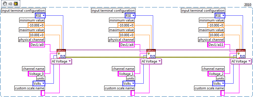


Maybe you are looking for
-
Satellite P300 - wrong display resolution
HelloI have Toshiba Satellite P300 and my display work stoppage last month, it does not display anything only turn on the light for a few seconds. So I buy a new and that display all but a bad resolution or Idont know what to see photohttp://ImageSha
-
one please. the 8600 workstation can be configured for efax
-
Just bought my new laptop with Vista already installed. Implementation has been good and security. Check my e-mail, but cannot open a simple Word attachment. Can anyone help? It would be greatly appreciated. Thank you Jay Cee,"Keep The Faith".
-
Hard drive WD3200BEKT is replaceable with newer model, the WD5000BPKX?
MINE IS HP PAVILION DM4 1009-UT. Hard drive WD3200BEKT is replaceable with newer model, the WD5000BPKX? Thank you