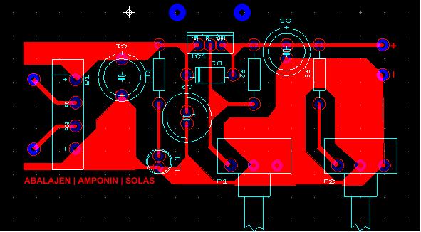
Ultiboard PCB outline
Hi all, I am new to Ultiboard and try to throw a quick Board together. I'm trying to remove the objectives of optical investment that appear in the upper left corner, bottom left and right corners of the PCB, as their size is disturbing given the bleached Board. Is there any setting or option in Ultiboard can I use to delete (because they do not seem to appear anywhere in the design of the actual card on any of the layers)? If it helps, I'm exporting to files Gerber RS-274 X. Thank you for your help.
These are the fidicials. You can delete them in the global Preferences.
- Click on Options > global Preferences
- Select the PCB design
- In the lower right corner, uncheck display guides
Tags: NI Software
Similar Questions
-
I would like to create a pcb using the Ultiboard layout. I want to do something similar to the one in the photo, but I really don't know how. It looks like a real pcb or as a manually done pcb layout. Could someone teach me how they did it?
Ahud,
You can use Ultiboard directly to create the PCB shown, but sometimes it is better to start with a diagram in Multisim firstly to define connections part/pin , then use the layout of Ultiboard PCB software to complete connections. By a schema first, all connections of each pin will be displayed with a connection "rats nest" - essentially a line telling you where to connect each PCB trace. If you want to use Ultiboard by itself, you will need to familiarize with netlist Editor (in Ultiboard menu, tools-> editor of Netlist).
I highly recommend a scheme of construction first. A simple tutorial that I created for users showing how to create a simple diagram in Multisim and end up generating a layout of the map in Ultiboard schema is attached. A part of the design is already done, but it should be useful in getting started. You will need to download and install the trial to start to use the tutorial.
Also, there are many other tutorials and getting started guides for Multisim and Ultiboard on ni.com/multisim here: http://zone.ni.com/devzone/cda/tut/p/id/5579
Kind regards
N Pat
-
Hi all
I'm having a problem with creation of UN ultiboard PCB. I placed a plan of mass on the top brass. In the classic view, it seems the entire PCB. In the 3D preview, it only covers certain areas... (Please see attached screenshot)
Any idea on how to make the mass on the PCB set plan?
I use the student Ultiboard 12 version.
Hey,.
I placed a request for corrective action on this issue, but until then, yes it seems that your work around is the only way to get this working. For manufacturing, file gerber should have no problem be it well, seems that only rendering is bad.
Thank you
-
How can I remove an existing model components?
I have an old drawing is updated. Several items have been removed from the schematic in Multisim, and changes have been annotated with impatience to Ultiboard.
The components were still available to Ultiboard PCB (all other programs I've used automatically deleted).
I manually deleted the components in Ultiboard. Now the DRC Ultiboard is telling me that the components are not in the design. No joke!
I see that these components are listed in the netlist in Ultiboard, even if they have been removed from the netlist in Multisim.
Apparently, Multisim fails to transmit new information to netlist to Ultiboard with before annotation - what is quite poor, because it is the object of an annotation before transmitting the design changes!
How send netlist update of Multisim with Ultiboard?
PRH
V11.0
Hi PRH.
The component should be removed, but try this:
In Ultiboard, select Tools > Netlist Editor, click the Remove button, and then select all your nets and delete them. Components and traces should remain. Now try before annotation of Multisim.
If this does not work, I like to look at your file. If you can send me a private message with your email address and I will contact you.
-
Ultiboard: Cannot stop component outline
Even when I disable the visualization of all the layers except the current, I still see the outline of all the components on the circuit board. They are always there when I move the active layer to another layer thus and disable the visualization of the current previous layer as well.
I remember ever turn on an option to visualize the contours of component and you don't see any option for during such a thing that I look at all the different options.
I use Ultiboard 11.0.2 with Windows 7
Is attached a screenshot of the problem.
Hi Rick,
The outline on the parties just shows that they are currently locked. If you click with the right button on the outline and select unlock, the outline will disappear.
-
importing a dxf to the outline layer Board of Ultiboard
I try to import an outline of the map of another CAD file, but I have several problems. First of all, with the layer "Outline of the map" selected, if I import the .dxf file it place in white color, while this layer must be yellow. How to convince Ultiboard is the outline of the map?
My outline of the map also has a semicircular path in its perimeter; the entire Board is rectangular, but there is an outline of a semicircle on the side. When I import the .dxf, it comes out as a full circle. So no idea what is the problem?
Thank you
Hi Jweaver,
When you import an outline of the map, Ultiboard to import the settings of the DXF file, including the color layer. Often, this color is white in AutoCAD, and so when you import the file, the layer of the Board outline is white. You can check in the Toolbox of design and also change color to yellow.
Import DXF in Ultiboard has some limitations, which is probably why import is to convert the semicircle to a full circle. The next version of Ultiboard has some difficulties to import DXF, and unfortunately, there is nothing you can do until then. However, I encourage you to post the file DXF here so I can see if the problem is resolved.
-
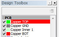
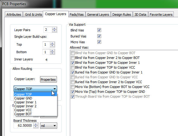
Layers PCB changing on MultiSim annotate with impatience to Ultiboard
I'm under Ultiboard and MultiSim Power Pro v 10.1.1 (10.1.372)
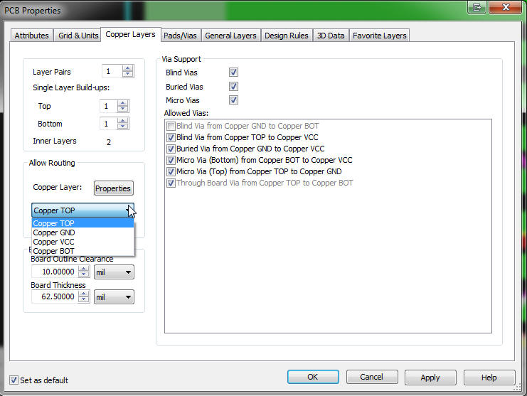
I have this definition of the Ultiboard copper layer:
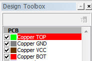
and the Toolbox of design in Ultiboard is:
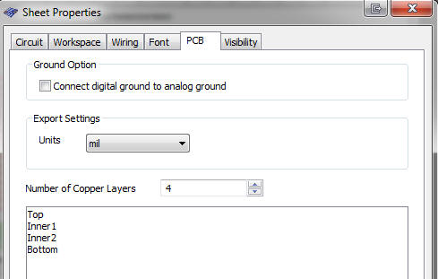
I have 4 layers defined in MultiSim, but is the only option for a tray of 4 layers: Top, Innner1, Inner2, down like this:
If I do my layout, addition of microvias and buried vias, all is well until I send annotates of MutiSim. Then my diapers in Ultiboard change 'automatically' to:
and all my microvias and buried vias to disappear! I can change the properties of PCB in Ultiboard turning pairs of layer to 1 vs 2 and recheck the vias I want and it's to the right layers but my microvias and buried vias are gone forever.
How can I stop this from happening?
-
I can't get rid of the layer names in the general properties tab layers PCB Ultiboard
A bunch of DXF layer names have been concluded by Ultiboard 10.1 error a few years during a DXF for import operation. I have recently updated to 12.0 and hope that the old layers would be eliminated. I wanted to get rid of them for a long time. I tried to delete the file ub_config in AppData, but it didn't remove them. Is that all you can think to extract them from the clutches of the program? Thanks, Tod
Hi Tod,
I suspect one of your design files is the cause. If you go to Options > CFP properties > general Layers, you see here DXF layers? If you see the layers, you can select it and then press the delete button?
-
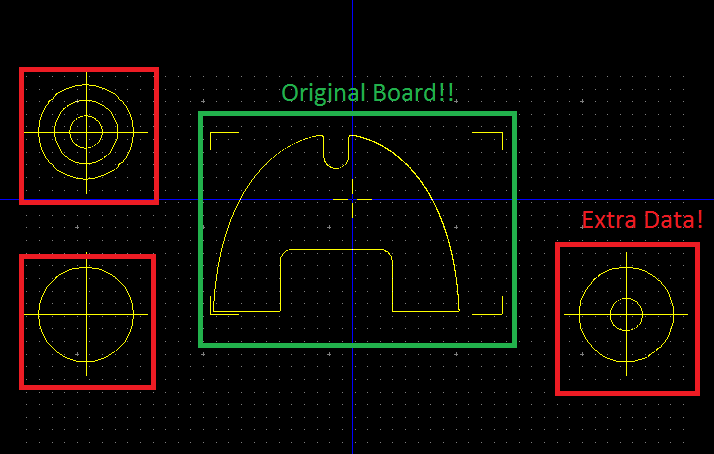
I see additional data when I export the outline of the map of my design as a file gerber
Hello
Whenever I have export files gerber my project and use any viewer Gerber to check my design that I encounter the following error. In the outline of the map layer, and more the contour of the actual card, one would expect to see, I see three additional points around the Board. These circular marks seem to have added around my board every time I do an export using Ultiboards built on the basis of export. I enclose a snapshot of the look of my layer of the Board outline and you can clearly see the three circular spots around my Board of Directors. I also enclose my main project for your comment file. Any help will be appreciated.
Thank you
RD
Hello
What are the alignment markers.
If you don't want them, turn them off:
go to the OPTION menu
the global preferences
On the PCB Design tab, you will see a box with the post-processing
Here, you can turn off snap lines
success!
-
Problem in import of DXF files in version education Ultiboard 11.0
Hey guys,.
Use Ultiboard 11.0, the education version. Trying to import a DXF file designed in solidworks for my PCB. The DXF file
also one through a molex connector that has already drawn in solidworks and actually fits. The problem is,
How can I create a real fingerprint THT this connector using the holes that are already in the Board outline. Also wonder what
the problem might be because when I import the file as a contour of the card then in the mode of the print edition, the sketch does not need to be
chosen or even modified. What is a limitation of the circuit design suite education edition?
Hello
First take a quick lok at this, it's a KB on the import of dxf files.
http://www.NI.com/white-paper/13722/en
If it's all for you so, can I get more details about this issue? The DXF files and your work ultiboard would be ideal to start to see what I can do to help you. There are many things that you need to support importing DXF files (take layered account, connections, etc.) and sometimes it raises problems of compatibility, but there is no limit with the educational version about the import/export of dxf files.
Kind regards
-
Hi all
First time poster.
Noob question type to come.
How can I get the highway as a single face KIC Ultiboard? Unless I got it completely wrong, that you have only a minimum of a top and bottom copper layer that is a double-sided Board. I will make my own pcb and do not want to use double-sided.
It's as simple as saying to not use through any description or who is a little brutal method?
In addition, anyone know of any software that will be the pattern of multisim and highway a veroboard/veroboard layout?
Thanks in advance.
Karl.
You can mark the bottom as layer cannot be routed.
- Click Options > properties of PCBS.
- Select the layers of copper
- In the box allow routing, select the bottom copper, and then click Properties
- Uncheck the Routable
If you have a version with layers of PCB in the worksheet, you can also make this a little easier.
- Click the tab layers PCB in worksheet view
- For copper, change routable on the No.
-
Ultiboard DXF to Gerber Polylines do not convert to polygons
Hello
I am trying to import a DXF to ultiboard antenna file and export it as a file gerber. The DXF has two layers, edge contour and copper, I chose merger to the Board outline and the copper top. I also check the option "Convert polylines, polygons", but when importing, there is no area of polygons/copper, just as traces of copper imports as you can see in the screenshots. No idea why the polylines are not convert? Dxf was generated from solidworks, so I am confident that the pads are closed areas. At the bottom of the antenna, you can see there is even a text (part number) which clearly would be closed, but is not a conversion.
This article is basically said to check the option "Convert closed polylines to polygons" during import, which as I said, did not work for me. But for anyone else having this problem, I solved it by editing the dxf file so that areas of copper I filled, were met. Then when I imported dxf updated the ultiboard, they properly imported as areas of copper regardless of whether or not the option "Convert closed polylines to polygons" was checked.
-
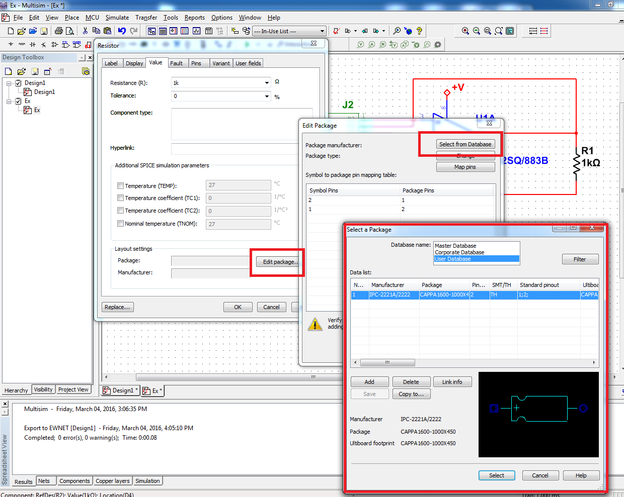
Missing components in my file Ultiboard if I transfer my file Multisim
Hello!
I am after this Introduction:
http://www.NI.com/white-paper/10710/en/?CID=Direct_Marketing---em80795&espuid=CNATL000018702741
On the point
5. the part D: transfer to PCB Layout
"" (8) select transfer "transfer to Ultiboard ' transfer to Ultiboard 13.0 and save the netlist file. Ultiboard opens automatically
This pop window ups:
Components with no package will not be exported.
See the results tab in the spreadsheet for a list of these components.Continue with the transfer?
I press ok, and my thread Ultiboard opens.
My resistance do not appear in the file ultiboard.
Any tips?
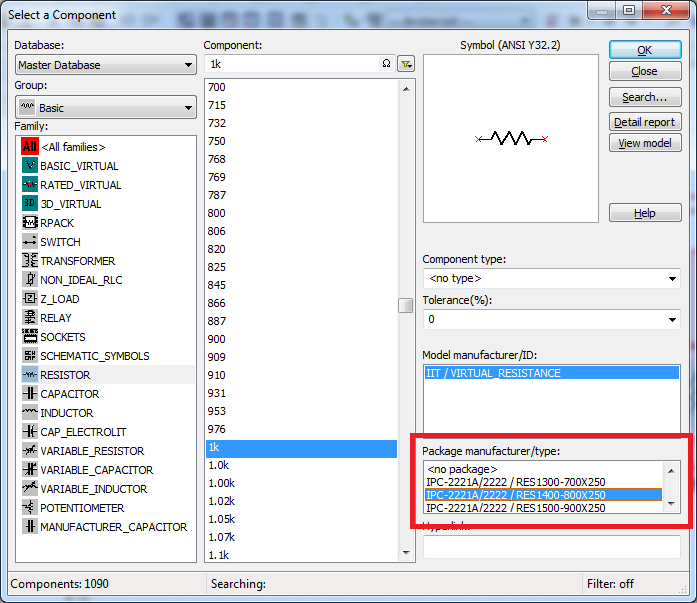
By default, when you place the RLN base, it has no assigned package. The package contains to Ultiboard layout information. Is this the message you saw said you, that the list of components in the spreadsheet was not exported to Ultiboard because they had no information about the package.
If you want to be able to transfer your RLC to Ultiboard components, you can choose a package when placing it down on the diagram:
Or you can add a package to a component that you have already placed. Double-click the component to open its properties and click on the tab 'value '. From there, you can edit the component package and select one in the master's degree, business, or the user database:
Let me know if this helps.
See you soon!
The f
National Instruments
-
Multisim for transfer Ultiboard Glitch
Hello
We have made many PCBS using Multisim as our software for schematic capture and Ultiboard for layout. The last room back does not work because the netlist in the schema is incompatible with the netlist in the provision of one piece (which is used several times on the map). Not only all the pins are reversed, but one of the pins is quite non-connected. Since the 8 pins are connected to the schematic side, this clearly isn't simply a matter of mixed up of PIN, but when I annotate with impatience, it is said that found no difference.
I went through and double and triple checked the symbol, the footprint and mapping of the PIN, and everything is OK. As a witness, I created a new schema with nothing else that the part in question and transferred to Ultiboard, and everything was OK.
Everyone knows about this problem before? This is a known bug and is there any workaround or recommended solution to avoid something like this happening in the future (outside routing by hand and without taking into account the ratsnest altogether).
Thanks in advance for the help!
CDM,
Please contact our support group. You should not see this question in v11.0. I'm not aware of the important issues with annotation front/rear, since we redesigned the annotation capability and improved reliability in v11.0 (from 10.1).
http://sine.NI.com/apps/UTF8/NICC.call_me -> select ask support
Kind regards
Pat Noonan
-
Formate Ultiboard Enterprise support export Valor ODB ++?
This question relates to the request of the House of PCB Fab I treat for an export format that works with their new Aegis 'CircuitCam"System. are there characteristics "additional export format" in the Enterprise of Ultiboard version?
Thank you very much, Tod
There is no 'Ultiboard Enterprise' version, so I'm not sure that you are trying to compare the versions, but there is no export ODB ++ to Ultiboard.
See the NI Ultiboard Professional product features for an overview of the professional features.
Maybe you are looking for
-
New native App Crasing on iPad Pro 9.7 "with iOS 9.3.1
The native application of News will not open. He flashes open for about a second and then closes. I tried: Restart the iPad. Two reset buttons (Home + Wake/Sleep). Forced to quit smoking (double tapping home + Drag upwards). Backup and restore. I wou
-
M10 Pro must restart couples to start.
Hello. I have a Satellite Pro M10. The problem with him is he doesn't start, it gives me the TOSHIBA logo only and it stops there. I have to restart it 3 or 4 times then it will display the Window XP logo and back to normal. Help please!
-
Re: Satellite M305D-recovery by default for Vista using recovery
I have the Satellite M305D-S4830 and try to restore the factory settings, the computer brings two DVDs, which applied well, but at the end of the second error 10-FC12-0241 number and asked to push a button to turn off the computer. So far I have not
-
Compilation of Simulink with the model interface toolkit (MIT)
Hello I am considering using the template Toolkit Interface to Simulink model in the LabVIEW environment. My question is about the process of compiling Simulink. To correctly compile the Simulink model in a DLL and then wrap it with the API from MIT
-
Can I switch window 32 bit of 64 bit Windows?
Upgrade from 32 bit to 64 Hello, I'm upgrading to Vista Ultimate 32-bit 7 Pro 64-bit. And I just bought the upgrade. Or did I have to buy a full version of Windows 7?