Block of RAM in SMU-7965R
I use the element of memory in my fpga code. However, it uses a lot of fpga slices eventhough I chose the memory implementation of the issue of the memory block. I though it should use block of RAM instead of other fpga resources. The number of total slices increases I increase the amount of data in the element of memory. It seems that using slices of fpga. I joined the project in LabVIEW FPGA and FPGA VI with this post. The target FPGA is SMU-7965R. Thank you for your help
LabVIEW FPGA needs to logic on the fpga to take care of the communication between the chip and your host, as the communication of control/light, logic of installation for the dma channel. While LabVIEW FPGA offers ease of use, there is a fee to pay. For most of the time, this cost is acceptable compared to your actual application.
Tags: NI Software
Similar Questions
-
NEITHER SMU 7965R for emulation
Hello
I want to develop applications for RIO Flex NI SMU 7965R in emulation mode as I do not have any hardware connected to my system, but creating FPGA project that I select Create new system whereby only the PXI-795xR series is available. How can I get the objectives of series PXI-796xR for my project?
As after testing in emulation mode I will run this application in the other system where SMU 7965 FPGA board is connected, so that I can directly export the project to the other system otherwise I can export only the VI where I should create new project under which I will add elements of memory needed each time.
Thank you
Chandrasekhar R Polska.
I found the solution to the problem of updating to NI RIO 3.3.1 which can be found using the following link
http://Joule.NI.com/nidu/CDs/view/p/ID/1528/lang/en
Now I can find maps of the series x 796 SMU for emulation.
Thank you.
-
Move from LabVIEW FPGA block of ram address to node CLIP?
Hello
I need to pass an index memory RAM of LabVIEW FPGA block to a CLIP node to the node CLIP to have access to the data in the BRAM. The node of the ELEMENT contains an IP address that we developed and the IP address is the use of Xilinx BRAM driver to access data. I guess that we need to move the physical address of the BRAM to the ELEMENT node.
Is this possible? If so, how? If this is not the case, what would be an alternative?
Thank you
Michel
If I understand you correctly, Yes, you should be able to use the memory block of the Xilinx pallet Builder in LabVIEW FPGA and in the loop of the single Cycle, connect the ports of this block signals CLIP exposed by the IP of your colleague. You may need to tweak/adapt some of the signals slightly to the LabVIEW data flow.
-
Only the 32 block RAMS and always showing error 3 used
Hello
I work on Photons counting upon arrival at DIO0. Short cut, there is a lot of data to come and I need to send it to the host as soon as possible. To do this, I used a FIFO extended target in a loop timed under unique bike and another target host FIFO taking this extended FIFO target data and send it to the host.
According to the analysis that I did, I need FIFO to 600 000 elements Boolean deep target. This should be possible since I use an FPGA virtex-5 wx30 FPGA which has 32 (36kbits) block of RAM. However, when I increase the number of items in this requested FIFO, compiling just can't say that code does not fit into the FPGA while it shows that only 3 of the 32 RAM block have been used.
I tried to search a lot on any restrictions on the FIFO, but I have not found.
Please help me here earlier.
I have attached the file VI and the sheet of newspaper of Xilinx compilation.
There are 6 FIFOs in this project:
The target host DMA (items I32, 1023)
Target to host DMA (Boolean elements, 2000)
Target to host DMA U32 (U32, 500)
Range of target DMA write (I32, 16000)
County of DMA scope target (Boolean elements, 108000)
DMA County U32 brought target (U32, 500)There is a bug in the compiler to Xilinx that not all types of block instantiated Rams are reported.
I did a similar discovery before. http://forums.NI.com/T5/LabVIEW/FPGA-block-RAM-FIFO-resource-usage/m-p/2978897/highlight/true#M85572...
Therefore, simply ignore the statistics of the compilation, they are wrong.
Block of RAM is not addressable as 36 k x 1 bit, it has 36 bit width or width 72 bits. This means that 1-bit, 2 bits, all the way to the top 36-bit all fill a cell block of RAM.
Therefore, your consumption will be 600 k x 36 bit which gives much more than what you're supposed to be bit 1 x 60000 storage trequirement.
1x600k is part of the block of 32x36k RAM (600 KB required, 1 MB free space)
but the reality is that
36x600k does not fit in the block of 32x36k Ram (21 MB required, 1 MB of free space).
If you can, try little racing Booleans in one FXP 36 bits before writing in the block of RAM will improve you things.
-
Coregen memory when you use defined VI block memory
I currently have a problem when you try to compile a VI for my card Flex RIO (SMU-7965R). I have a sub - vi which contains a small instance memory set by VI (U16 X 256 elements) and a block of DSP48. This VI is instantiated 128 times in the top level VI. When I set up the memory set by VI to target the block of RAM in the FPGA, the compilation process is suspended during the generation of the nuclei (memory after ~ 45 min). LabVIEW treats each instance of as single block memory when executing coregen? I do not experience this problem when I set up the memory set by VI using LUTs. Any thoughts would be appreciated.
Thank you
Brian
Hi Brian,.
I believe that this compilation failure could be less related to the implementation of memory coregen, rather the memory of the way that is implemented in the lut and block memory on an FPGA. Lut are built through flip-flops and are perfect for storing information 100-300 bytes, while the memory block is segmented in a fixed size of 2 k RAM embedded. There are only a number of structures of block of RAM in a given FPGA and it seems that in your case that you use more of your resources block of allocated RAM. For example, in the 7831R if we tried to implement a FIFO in the maximum possible storage size block memory would be 81 920 bytes due to the limitation of resources.
The implementation of flip flop of the LUTs will allow the compiler greater flexibility in the use of resources in compiling because the size of the LUT is not fixed in the way that is a block structure of RAM. This is probably the reason why this LUT implementation is compiling successfully while the RAM block is not in this case.
Kind regards
Blayne K
-
1066 MHz RAM for MacBook Pro 2012
Hey guys!
Just registered here, I hope you can help me.
I have a MacBook Pro (mid-2012) that shows the problems that resemble RAM errors. The 2012 version uses DDR3 1600 MHz modules.
I can get my hands on a model of 2009 with the DDR3 1066. I intend to move blocks of RAM to see if that fixes the problem with the computer of 2012.
So my question is:
The MacBook 2012 will work with 1066 MHz RAM installed? (Provided that the RAM was the culprit, of course). If so, will there be problems other than lower performance?
Thank you!
Terji
MacBook Pro are very sensitive to the Ram being the correct specifications for the computer. Your computer is designed to use only the same characteristics for RAM Why would you think clock speed of 1 066 MHz RAM work in a 1600 MHz system?
-
Re: Satellite L20 - SLOT of RAM configuration
Hi, my L - 20 Satellite has a memory of 512 mg installed, I buy anti-spam memory ram of 1 GB to increase my memory and put it in the second slot.
This block of RAM works well because I remove the old block of 512 MB and put it in the biggest and the BIOS recognizes it well.BUT, if I put the block two ram, BIOS recognize only half of the block of ram 1 GB, if in addition it recognize 1 GB total RAM instead of 1.5.
data sheet says that the 2 RAM slot can be level up to 2 GB, but one of them 'configuration '.How can I configure ram Slots? There is nothing in the BIOS
Please help me
Gherardo
This slot machine configuration doesn t exist and if you use compatible RAM modules it will be recognized correctly.
Can you please give us more info on this 1 GB RAM module?
-
Hi all
How to set up a memory block maximum size on my FPGA target and what size of memory allocated?
The Documentation States:
NI PXI-7853R : built-in memory 384 kB
Short form : block Embedded RAM 3 456 Kbps
384 k = 393216 bytes
3456 kbit = 432000 bytes
What is the problem here?
Memory project FPGA Configuration dialog box
DataType U8
"Asked the number of items": maximum of 4294967295 (stays of value even if you enter a higher value, seems to be a 32-bit overflow)
Number of items: 134217728 (no idea what means the number).
I'm just assuming that 393216 or 432000 is the maximum. number of bytes?
Finally, there is a build error (error of xilinx) about the size of the ram, if the number is higher.
However if there is no error (for example using 393216) generation (usually 10 minutes) proceeds ' generation xilinx ip "within 15 minutes.
I don't want to continue to guess, then, what is the number I enter the memory maximum memory Configuration dialog box?
Concerning
Christoph
Hello ChristophSauter,
The maximum number of items that can be created in one memory FPGA PCIe-7854R card when you use U8 is between the 442368 elements and 393216 according to optimizations that Xilinx LogiCore block memory generator Minimum area algorithm can do.
The cylinder block Embedded is 3456 Kbps-> 3538944 bits
But it is continue to know how many ram blocks block exist and what data you want to write in memory, it is possible that the 8 bits of data use 9 bit in memory. Overview of the Virtex-5 familypage 2 XC5VLX85 is the FPGA and the information on it.
I hope this helps.
-
Upgrade of RAM - I have the part number, but what is?
Hello
I have a T61 with 2 blocks of ram with 521 MB each. It must be replaced by the 2 GB module if possible. In search of Lenovo pages, I know that the modules of machine Ram is "512MBPC25300NP".
Which means that the acronym for? What should I look for when looking for a new 2 GB module?
--
You must look for DDR2 PC2 5300 667 Mhz 200 pin SODIMM memory, for examplethis. You can use any generic RAM meets these specifications. There is no need to pay for what is called memory "premium". I buy everything that is cheaper and have never had any problems.
DDR2 SDRAM explains what the average numbers. (Note the ESL 200-pin SODIMM is a variant of DIMM 240 pin.) The first is designed for laptops while the second is for desktop computers).
-
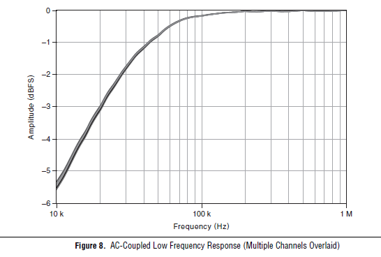
[fpga] Configuration of analog input or 7965R
Hi all
I have a card FPGA NI FlexRIO (SMU-7965R) with an adaptation module (NI 5733). I'm using Labview real-time 2012. My measurements are dominated with harmonic sound of 60 Hz, which is most likely due to the ground loop. I try to put my analog inputs (as opposed to the CSR, NRSE) differnetial mode to try to overcome the ground loop. I came across this link which explains how to configure the FPGA input channels-
http://digital.NI.com/public.nsf/allkb/08EF26D2E9041BC6862570E0001E442E
However, the installation program of the RIO device for my goal of opening, I found that there is no option to choose the channel configuration (as shown in the attached picture). This means that the analog channels are in differential mode by default? If this is not the case, how can I change?
Any help will be greatly appreciated.
Hello!
This KB is in what regards R, not FlexRIO product line series materials. I know it's a little confusing because the 7965 has an indicator of 'R' at the end of the model name, but the R simply it is a product with an FPGA that is programmable by the user.
Unfortunately, the adaptation modules FlexRIO 573 x are all only ended then we will not be able to change to the differential. What is the frequency of the signal you're trying to measure? Another option would be to set the 5733 coupling AC mode, which would give the frequency response following, dramatically eliminating any sound below 10 kHz.
-
RAM for Vista problem shows only 1 GB despite 2GB material
I have Windows Vista 32 bit installed in my system with 2 GB of RAM, and it worked perfectly. Yesterday my system performance show only 1 GB of RAM and the Ram usage is 60 to 90% of the capacity, I know that max support 4 GB 32-bit system, but how is it ' show only 1 GB? I checked the RAM blocks separately in each lazy and they both works perfectly, yet, it shows only 1 GB? What to do? It's like Vista only uses one of my blocks of Ram.
Memory of rum diagnostic test:
Memtest86 + - a Memory Diagnostic tool
http://www.memtest.org/Swap the memory sticks and try to start from with one stick in the slot. Do this for both sticks of memory the. /
-
Programmatically, returned the error code 31
Hello
I use NI PCI-5640R and NI PXI-5600 with Labview 2009. When I compile my FPGA VI, I get the following error message:
"At AU!
ERROR: Xflow - returned programmatically code 31 error. Aborting the workflow execution... "Could someone guide me what what is this error and how can I remove this error?
Thanks in advance,
Rashid
Hi rachid,.
There are actually quite large differences between the FPGA on the SMU-5641R and the card PCI-5640R. The 5641R has 640 multipliers and 8784 KB block of RAM, while the 5640R has only 136 multipliers and 2448 KB block of RAM. In my view, that the significantly smaller FPGA on the 5640R can't handle the FPGA VI without modification on the FPGA VI. In order to perform the build on the 5640R, you will need to cut some of the mathematical operations in requiring code of multipliers.
-
Transmission of data to the host of RT to the FPGA via DMA FIFO
Hello
I try to write data from a host of RT on target FPGA using DMA FIFO and then process these data and read then return of the FPGA target to the host of the CR through an another DMA FIFO. I'm working on the NI SMU chassis 1062 q, with the built-in NI SMU-8130 RT controller and target FPGA NI SMU-7965R.
The problem I face is that I want to send three different tables, two of the same size and the third with different size, and I need one more small to be sent first to the FPGA. I tried to use encode dish with two executives in the FPGA VI. In the first image, I read and write the first table in a while loop which is finite (that is, a finite number of iterations). The second frame contains the process of reading and writing the second two tables (of the same size) in a while loop that can be finite or infinite (depending on a control). The problem is that it does not work. 2 arrays are displayed on the front panel of the RT VI host and works well, however, the table that should have been read in the first sequence does not appear on the front panel of the RT VI host. It is not sensible because if it is not passed from the host to the fpga and vice versa then the second image should not have been executed. Note that I'm wiring (-1) for the time-out period to block the while loop iterations until the passage of each item is completed. So the first while loop has only 3 iterations. Could someone help me undersdtand why this happens and how to fix this?
I enclose a picture of the host and the fpga vi.
Thank you.
If you vote for my idea here and it is implemented, you can even omit the loop FOR fully.

(I also propose the RE / IM divided inside the loop FOR and perform operations on complex table before the loop the transpose and reshape .) In this way, you only need one instance of these operations. You might even save some unnecessary allocations table in this way)
-
LabVIEW FPGA Module 2015 Compilation to PXIe7820 with 'no timetable '.
I did a first compilation for the SMU with the Xilinx Vivado 2014.4 tool 7820 (64-bit). Compilation report said.
Compilation successfully completed.
Use of the device
---------------------------
Total bands: 19.1% (25350 4848)
Records of slice: 6.9% (13937 on 202800)
Slice lUTs: 12.3% (101400 12430)
Block of Rams: 0.9% (3 out of 325)
DSP48s: 6.2% (37 out of 600)Calendar
---------------------------
None.Compile time
---------------------------
Introduction date: 16.07.2016 12:48
Date recovered results: 16.07.2016 12:59
Waiting time in the queue: 00:08
Compilation of time: 10:16
-Generate a Xilinx IP: 00:00
-Summarize - Vivado: 04:18
-Optimize the logic: 00:14
-Place: 01:17
-Optimize the Timing: 00:18
-Road: 03:04
"- Generate the programming file: 00:56.This means no timetable? The embedded clock's 40 MHz. It runs with this clock? Beacause 7833 compilations for the pci or pcie 7842 report displays the maximum clock time.
Hello
"none" means simply from what I can understand, that there is no violation of timing. The source of synchronization that will be used is (as you have already suspected it) on-board 40 MHz clock.
As to why you don't get a mention of the MiteClk and the ReliableClk in summary, I think that it is due the 7833 and the 7842 relying on FPGA Virtex-II and Virtex-5, while the 7820 uses the Kintex-7 family. Depending on what type FPGA using different estimates regarding the use of the device and synchronization are not always available.
As I said, as long as you don't get not an error of timing and your compilation is completed successfully, you should be fine.
Kind regards
Alex
-
Tecra M3 started slowing down, cursor becomes too slow and then freeze. The POST screen is any value, but the start being different garbage which allows to see which line start (safe mode) options. Problem seems to be thermal associates who sometimes, system start-up cold upward but 90% of the time, no display on LCD - only with external display connected. Will continue to auto restart until a successful boot that sometimes takes hours.
Windows XP on startup has fourteen vertical lines in ten columns (blocks of RAM) However, today, the thermal problem spilled in that it starts better when it is hot now! I am a technician in electronics and the problem seems to be a video RAM hardware fault. Someone else had problems like that? My biggest problem is having to go the laptop while our IT Department it sorts and possibly get it he returned after having wiped clean or not at all!
Hello
I agree with you. It looks like a chip of the graphics card would be malfunctions.
Maybe the cooling modules don't work properly and can not cool the GPU in the right way!In my opinion, the service provider must be contacted for a detailed audit.
Technicians authorized in your country could begin to some test procedures and found the flaw easily.Good luck
Maybe you are looking for
-
Firefox is no longer makes type in my fonts - upgrade problem?
I have my fonts preferences set to display Serif fonts, specifically Times New Roman, and 'Allow pages to use their own fonts' is not checked. However, all pages that I charge rendered in a font without serifs. I have a vision that makes lineales pro
-
Where to buy drive HARD MK4019GAX for Satellite Pro 6100?
Hi - I need a new hard drive for my satellite pro 6100, MK4019GAX part number. I have searched online but have drawn a blank. Any help would be appreciated. Thanks, Roy
-
My laptop screen does not work
Hello Sir/Madam, My laptop HP nc6400 does not screen and also does not have much time for backup battery. So, I can not able to work in that. So please kindly help me to find a solution to these 2 problems. Thank you best regards &,. Aminatou M.
-
Whenever I click on a site it redirects me to another
whenever I click on a site it redirects me to another sick e.g. click on facebook and I go on me on another site please help
-
Volume icon is not displayed in the notification area in the Windows XP machine.
Original title: Volume control. The icon that appears in my system volume taskbar is no where is easy to make adjustments of volume control a chore. Not what I want to do. What can I do to fix this?