Design of FPGA
Hi, I want to use the object - oriented program for the FPGA, programming wil FPGA control a pump to create pressure, is there as a consultant for the design template?
It seems that not all the features of LabVIEW OO are available in FPGA. I'm guessing that things like the dynamic distribution are not something that can be easily represented in the doors.
http://zone.NI.com/reference/en-XX/help/371599H-01/lvfpgaconcepts/fpgaclassesinvis/
http://digital.NI.com/public.nsf/allkb/376C9F5112F10A8C8625795A0059D2D5
I've never had need OO in FPGA. Generally OO is ideal for flexibility and always changing requirements, and for me an FPGA is usually a dedicated piece of hardware making a specified job that he can do in a deterministic way. These two things in my mind don't mesh well.
Tags: NI Software
Similar Questions
-
Is it possible to filter design on FPGA reconfigurable on the fly?
Hello world
I wonder if it is possible to design multi-channel filters on the FPGA reconfigurable on the fly? For example, it is possible to have X bandpass filters in an iteration, and Bandpass Filters Y with different specifications in the iteration following without having to recompile the FPGA code? Is there a simple way to achieve such a purpose?
I have built such flexibility in the OTR (where each iteration has different filter settings) but hope to implement on the FPGA so.
If someone could provide ideas as to whether or not such a conception is possible, it would be greatly appreciated.
Thank you in advance for your help!
Steven
Hi Steven,
How do you try to generate the FPGA code for this filter, you are using the IP generator?
If so, this knowledge base article describes fixing the coefficients for multichannel to change on the fly filters. There is also a nice example in there also.
Also, if you use this IP generator, this help document describes the more Options box that has the ability to change the coefficients to be 'rechargeable' so that you can change these on the fly it too.
-
Acquisition of data and filtering on FPGA
Hi all
I have trouble to design a FPGA program for acquisition of data and filtering.
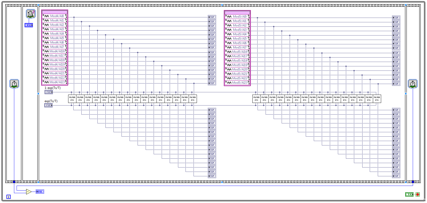
I have two NOR 9205 modules configured to work in terminal mode of DIFF, i.e. There are 32 entries this program must read every Ts seconds. (Ts is the time discretization, i.e. during the period of loop)
With respect to the digital filter, I implemented a possible simple filter with transfer function G (s) = 1 /(1+sT), which is part of the field of discrete-time equal to y (k) = a * u (k - 1) + b * y (k-1), where u is the original signal, and there is filtered signal. The coefficients a and b are equal to: a = 1-exp(-Ts/T), b = exp(-Ts/T), and T is the time constant of the filter (usually T > 5 * Ts).
The implementation of main program for the acquisition of data and filtering are:
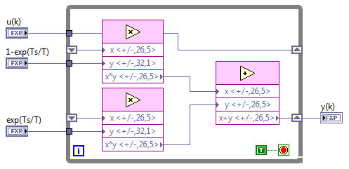
This application is for the digital filter:
However, the problem is that this program cannot take the FPGA resources on cRIO-9114, and Yes, I tried to define the criteria of compilation for the area. I also tried to implement the multipliers in digital filter as lut and DSP, unfortunately without a bit of luck.
Because I don't have that much experience in programming of FPGA, someone has any suggestions how to improve this code to adapt existing FPGA resources?
Best regards
Marko.
Hey Norbert_B,
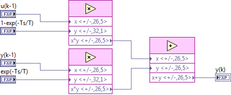
I managed to solve the problem. First, I changed the reentrancy of Preallocated incoming execution clone to not reentrant execution. As no reentrant VIs have States, I had to use the node of the feedback to the main VI to get u(k-1) and y(k-1). Another important thing is to choose Ignore FPGA reset method in the node of the properties of FPGA implementationfeedback, since in this case, the feedback node uses less resources.
Here is the new main program VI:
And here's the 'filter' VI:
Thanks for the help!
Best regards
Marko.
-
Camera Link image, line, data valid bit locations
Hi all
I'm trying to re-design code FPGA vendor to change a camera of 4 x 12 Medium to Full 8 x 8.
The Camera Link standard is quite confusing. The way I read it, a Camera Link of 8 x 8 Full camera should affect the valid as follows:
LVAL: bit 24 on three channels
FVAL: bit 25 of the three channels
DVAL: bit 26 on three channels
For some reason, the provider asigned them like this (and IT WORKS!):
LVAL: bit 18 on three channels
FVAL: bit 19 in all three channels
DVAL: bit 20 of three channels
There is another format that corresponds to the valid Bit arrangement? If so, is there something in the Camera File Generator and. Files of CIM which defines the format?
See you soon!
Crazy
Crazy,
Yes, you are right the LVAL, FVAL and DVAL are on TX/RX24, 25 and 26 respectively. These assignments of bits match with parallel interfaces on Channel Link Serializer/Deserializer chips. The PCIe-1433 expect that framing signals are mapped to the signals to the camera.
Not all cameras output a signal DVAL, so they can be ignored in the acquisition card (PCIe-1433) with a camera file parameter. In addition, the polarity of the signals framing can be reversed with a camera file affecting as well.
You may be interested in using Camera Link Logger with the PCIe-1433 to receive signals from the camera. Camera link Analyzer will present the traffic camera link in a format easy to read Visual format that can help your development and debugging.
http://www.NI.com/product-documentation/14301/en/
Regards, Jeff
-
Digital electronics FPGA Board Hardware Driver for Windows 10
My son just made me aware that his school has a dozen of National Instruments Digital Electronics FPGA boards, but they have never been able to get them to work or actually use them in the curriculum. It seems that he has left his instructor know that I worked with FPGA Xilinx for more than 10 years and now everyone counting on me to get these maps work. The issue seems to be the USB driver. According to the manual, I tried DEFB2012_5_2.exe which simply refused to run on this machine Win 10 x 64. DEFB_4_3.exe ran, but complained that LabView components have not been installed and that it would not continue. Could someone tell me please how to install USB driver ONLY so that we can download files of bits with IMPACT? In terms of a school budget, the investment they have in these maps is not negligible. Thank you.
Hello Dave and TGregor,
I hope I can clear some things here. I'm sorry that you run in so many questions with your boards OF FPGA.
First of all, direct responses:
The LabVIEW FPGA 2015 driver should install the components needed to use the Board with Xilinx tools on WINDOWS 7, it will not work on any system more recent that the pilot has been developed before the release of Windows 8 and 10.
http://www.NI.com/download/NI-Digital-Electronics-FPGA-Board-driver-software-2015/5857/en/
My recommendation for Windows 8 or 10 is rather install Xilinx ISE you find on Xilinx website or on the downloads page OR:
https://www.Xilinx.com/products/design-tools/ISE-design-suite.html
http://www.NI.com/download/LabVIEW-FPGA-Module-2016/6231/en/
The difficulty that you face here is that tool Xilinx ISE is officially supported only on Windows 7 and below. So even though I think it will work (and it will move to the difference in the link of the above driver OF FPGA) for Windows 8 and 10, you can continue to deal with certain issues.
Now you are all looking to program the FPGA using an HDL, Multisim and LabVIEW? If you just use an HDL, you should be all set to go and in the dev environment, you had planned using the program. Circuit design of Multisim 'S simulation tool which includes a complete library of graphic digital components. A digital circuit can be built using the graphical logic gates in Multisim then downloaded directly on the FPGA without first having to learn VHDL or Verilog. It is quite popular among the logical classes digital introduction and we can help you by establishes that as well if you are interested.
For anyone else who might stumble upon this page, I want to make sure you are all aware that, while the Board of Directors OF FPGA is still supported and sold, it has been developed a number of years and has recently been replaced by the Council for development of the digital system (DSDB)that uses a 7020 architecting and has much periphrials more to the program than the FPGA OF. So I know that it is not useful for the current issue, but anyone looking for if they would like to buy more OF FPGA boards, I recommend watching the DSDB instead.
Thank you!
-
Hello
I can generate a C API interface for FPGA design in Labview Communications.
And how does it work?
Thank you
Sebastian
Hi Sebastian,.
If it is anywhere in the LabVIEW Communications, he'll be in tools Launcher. If it is not there then you can still generate a C API for your FPGA using the FPGA Interface C API generator. I received this the generating a C API for a help Application LabVIEW FPGA Document.
Generating a C API in the Windows Start Menu
Follow these steps to generate a C API for a bitfile compiled in the Windows Start menu.
- "" "" Select Start "all programs" National Instruments "FPGA Interface C API" FPGA Interface C API generator.
- On the Generator of API C FPGA Interface dialog box that appears, navigate to the compiled FPGA bitfile or type an absolute path for her.
- Select a directory for output to the C API. If you do not select an output directory, the files in the C API will be created in the directory that contains the bitfile. You can navigate to a directory or type an absolute path for her.
- Optionally, you can change the prefix for the generated files and constants in the generated .h file.
- If you are using LabWindows/CVI to develop your C application, check next to exclude NiFpga.h/NiFpga.cas FPGA Interface C API installs the header and library files with the support of LabWindows/CVI.
Make sure you have installed FPGA C Interface API .
Introduction to the API of C Interface of FPGA
See you soon
-
changing/variable index of an array on FPGA
Hi all
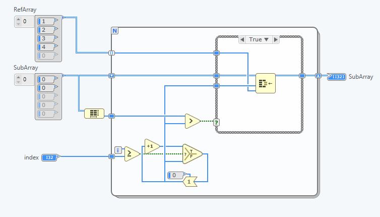
I have a question about indexing an array on FPGA. Concretely, I have a constant size 1 M table and want pieces of index of size N of it. Unfortunately, when you try to compile I get the error message: the tables with variable sizes running are not supported. Is there a work-around nice for who?
See you soon
Hello
Well, I don't have first play dynamicaly with the Index of the Array of subset function entry.
This is not supported in a SCTL, so that the planned behavior.
There are several workaround solutions to do this, depending on how you design your design.
1 point by Point approach (as usually made it in FPGAs), using a function table of Index on the RefArray and with the use of counters to keep track of the Index, and evantualy count each sample collected.
This means that every cycle, you have an example that needs to be addressed, you don't work with a tableau more out.
2. same as 1, but using a BRAM I32 element as an interface in the screenshot gave you, I understand that your table with a value of several KBs, which can be a problem in the long term for your design.
3. using a FPGA IP, you could build something like this:
You can use a loop in the context IP FPGA that auto-index the RefArray, to pick up the samples you want, in your sub-table.
This means that you can always work with a table in the output, but the cost will be that you can not leave the subarray in each clock cycle. (use the estimate feature to see the actual flow rate)
4. you can explicitly implement a big MUX, using a box structure. In each case, you provide the desired sub-table.
This is indeed what LV FPGA would do if you where using a standard while loop. Yes, ugly, but no way around it if you want a sub-table, at every clock cycle.
5. the BRAM/DRAM can work with an interface of up to 1024 bits, 32x32bits elements for ex, then you might have used up to 32 items in you case (using the loose I32)
So! In your case, I recommend that you use option 5 if possible:
-Think of BRAMs, your table is starting to get impatient on slices
-Use up to an interface of 1 024 bits on BRAM for a sub-table, do you really need more of 1024 bits a sub-table?
If you don't see how to go from there, I would need more information on what you try to do + all necessary and upstream of the stored data and their data type
Good bye
-
error 1136 When adding FPGA in SysDef
I have a PXI-7854R multifunction RIO installed in my SMU-1075 chassis. When I add it to the system under the FPGA node definition file, the RIO node is created with all its subnodes - as expected - but the attached dialog pop error. Whenever I highlight the node newly created Rio the same error appears. Everyone knows this?
I have an SMU - 6341 Multifunction DAQ designated as master hardware device Synch on the Bus 2 and moved to PXI_Trig0 through all three bus.
Also, I use Veristand 2011 SP1.
Thank you
Yes we have seen. Fortunately, it's just aesthetic. This happens when you have a DAQ master that is hidden in the tree and click devices FPGA. We hope to solve this problem in 2012. Sorry for the inconvenience
-
FPGA VeriStand personality is late? and latent FPGA data processing
I use a FPGA 7853 (only) in a SMU 1071 chassis with a controller 8135 and run VeriStand 2013 SP1. At the end of my test, I want to ensure the integrity of the test, which includes the audit of the FPGA interface is never late.
I first thought to expose the terminal 'Is?' late as a channel, but then I noticed it isn't really an account, it's just a flag. In addition, it seems that this flag is not locked, it does report by iteration of loop interface. This makes me think that I alarm an VeriStand on the later is for VeriStand FPGA interface design? channel. Am I correct, and if not, how NOR have I use East late? terminal?
As the DMA in the FPGA nodes then never expire, there no sense watching the Timed Out? terminals on the FPGA. But the effect of a timeout will appear in the East towards the end? Terminal Server. I'm tempted to change the end is? U64 to a real number in the number of late? the defined indicators synchronize to the host VI. is there a reason to not do this?
How VeriStand manages a FPGA end? If the RT side of the DMA buffer became more complete, data from the FPGA would be more latent, which could lead to the instability of the system. Hopefully the VeriStand engine should purge the latency of the data, but I don't see anything in the FPGA interface which would facilitate this.
Thanks for your help,
Steve K
Hey Steve,
If the PCL NIVS reads this flag as true, it incrememnts the County of HP system channel.
For the question of FIFO depth: The PCL is always expected to read and write a # fixed packages each iteration (as defined by the XML) and FPGA always reads and writes the same number of packets of each loop of comm iteartion and since the timeout is set to-1... orders may not be combined. Packets act as a handshake.
-
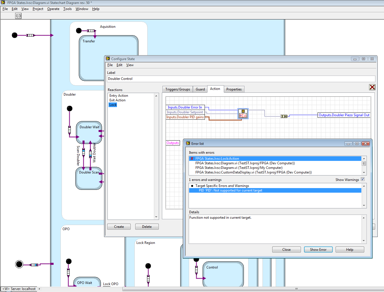
PID (FPGA) not taken in charge in an FPGA to States transitions?
I'm currently testing a PID (FPGA) vi in a statechart designed to run on the FPGA, but its gives me the following error. Am I missing something, or does the PID (FPGA) really not work when you use it in an FPGA to States transitions?
Thank you
OK, so it turns out that it is a confusing error message/situation. In fact, it is related to the autopreallocate parameter. If you drop PID (FPGA) on a regular VI in a FPGA target and clear the autopreallocation, the VI stops with the same error message.
Then to use PID in your custody/action States transitions, go to the Properties tab in the configuration dialog box, check the option to autopreallocate and drop the PID. LV will still show the error, because we do not change the setting of autopreallocate until you click OK. If you reopen the configuration dialog box, the error "not supported on target" should be gone.
I hope this helps.
-Nick
-
Option NEVER ARBITRATE for the same memory in both cases on FPGA in SCTL
Hello
I write code on FPGA and I wonder one thing. Maybe someone knows the answer:
(Example attached img) situation: I have a simple matter SCTL structure. If TRUE, I read elements of memory. In case of FALSE I read memory items even, too. There is only one exit from the structure of the case. Memory never arbitrate read option so I can compile the code.
Question: As on FPGA, runs the two cases, both memory try to retrieve data from the resource and give some output. In such a situation, it is good to put two instances of memory in separate windows in flat sequence structure so there is no danger (remember: never arbitrate option). So do the correct data when switching between cases? Or maybe, because of some risks, it is possible that I get incorrect data?
Thank you
The option never compromissory clause was designed specifically for drawings and models that use the template that you show here where there are multiple calls to the same method on the same resource , but where the code is written for any of the two appeals will be active at the same time. The implementation of material generated by the compiler is simplified to not wait as an active call which uses less resources. Only a single call comes at a time, inactive calls will not suffer from which affect the ongoing call.
That said, and as others have mentioned, for this particular simple example, pulling on the appeal of the case the structure is certainly a better option. But there are many cases where it might not be a viable option as in the example you gave where the initialization of the resource should be in a different location logically.
-
ERROR: TclTasksC:process_077: in the FPGA Compilation
Hi all
I use for my application in which I am facing following error when compiling my fpga code compact rio 9072:
Compilation failed due to an error of Xilinx.
Details:
ERROR: TclTasksC rocess_077: did not finish. Please, look in the newspaper and report files.false
When running
"process run"card.
(file "C:\NIFPGA\jobs\XI64xG6_My449tj\map.tcl" line 6)ERROR
ack:2310 - type compositions "SLICEL" too found to adapt to this device.
ERRORack:18 - the design is too large for the device and package.
Please see the Design summary section to see the cost estimates for
your design exceeds the resources available in the device.
NOTE: A file NCD will be always generated to allow you to examine the mapped
Design. This file is intended for assessment use only and will not be processed
successfully through NOMINAL.
This NCD mapped file can be used to assess how the logic of the design has been
mapped in FPGA logic resources. It can also be used to analyze
preliminary to the level logic (route pre) calendar with one of the static electricity of Xilinx
analysis of synchronization (PRHT or Timing Analyzer) tools.
Summary of the design:
Error number: 2
Number of warnings: 69
Use of logic:
Number of slice Flip Flops: 7 886 on 15 360 51%
Number of 4-input lut: 16 104 on 15 360 104% (OVERMAPPED)
Distribution of logic:
Number of slots occupied: 8 744 7 680 113% (OVERMAPPED)
Number of slices only related logical container: 8 744 100% 8 744
Number of slices that contains no logical relationship: 0 to 8 744 0%
* See NOTES below for an explanation of the effects of unrelated logic.
Total number of 4 input lut: 17 400 on 15 360 113% (OVERMAPPED)
Number used as logic: 15 998
Number used as a middle way: 1 296
Number used as Rams 16 x 1: 82
Used number recorded the shift: 24
The logical Distribution report slice is not significant if the design is
too mapped to a resource not slices or if Placement fails.
Number of IOBs servile: 183 on 333 54%
BIO flip flops: 74
Number of RAMB16s: 1 24 4%
Number of MULT18X18s: 2 on 24 8%
Number of BUFGMUXs: 4 to 8 50%
Number of DCMs: 1 on 4 25%
Fanout of the Non-horloge nets on average: 3.38
Peak Memory use: 361 MB
Total in time REAL in the completion of the card: 1 dry 12 mins
Time CPU until the end of the total map: 1 dry 12 mins
NOTES:
Related logic is defined as logical that share connectivity - for example two
Lut are "related" if they share common inputs. During Assembly of the slices.
Card gives priority to combine the logic that is related. Generates so
best performance of synchronization.
Without logical report does share no connectivity. Card will start only packing
logic not related in a slice once that 99% of the slices are held through
logical packaging partners.
Note that once the logical distribution reaches the level of 99% by related
logical packaging, this does not mean the device is completely used.
No logical report package will begin, continuing until all usable LUTs
and FFs are busy. According to your timing budget, an increase in the concentrations of
logical packaging unrelated can adversely affect the performance of timing set
your design.
Mapping performed.
See the report of map file "toplevel_gen_map.mrp" for more details.
Problem encountered during the packaging phase.
Failure of the process 'Map '.Start time: 18:29:23
End time: 18:44:42
Total time: 00:15:19Can someone tell me why this error came?
Thank you best regards &,.
Vipin Ahuja
Vipin Hello,
It seems that your code requires more resources that are available on the FPGA. Optimizing your code can help to solve your problem:
You may have noticed some "Overmapping", mentioned in the newspaper:
Number of 4-input lut: 16 104 on 15 360 104% (OVERMAPPED)
Distribution of logic:
Number of slots occupied: 8 744 7 680 113% (OVERMAPPED)Take a look at this article:
http://digital.NI.com/public.nsf/allkb/060BA89FE3A0119E48256E850048FFFE?OpenDocument
And this:
http://digital.NI.com/public.nsf/WebSearch/311C18E2D635FA338625714700664816?OpenDocument
Kind regards
Navjodh
National Instruments
-
Synchronization of multiple FPGA PID loops
Hello
I am the design of a PID controller for each of the three axes (X, Y and Z) of a piezoelectric stage using the FPGA module and a cRIO. I used the example of project "Using Discrete PID - cRIO.lvproj" (labview\examples\control\pid\fpga.llb\CompactRIO) as a starting point and I've basically added two PID loops more on the FPGA VIs to the other two axes. I can get the controller to work for an axis at the same time (in simulation mode), but whenever I try to run all three controllers simultaneously, only one works. In order to synchronize between the host and the FPGA VIs, I used three interruptions for each PID loops, but it seems that a single interruption works when I run the code... No idea how to synchronize the three loops of PID with the host VI?
Kind regards
Shin
I think that it is an expected behavior, by the documentation: "VI the interruption is a shared resource, so multiple uses of it induce a further delay and jitter due to arbitration." If you are waiting for the interruption to see, then the other loops cannot continue because interruption VI does not work. On the FPGA if you want all the PIDs to operate at the same speed of loop, put them all in the same loop and use only a single interruption. Or use another synchronization mechanism (set to a boolean of the host, wait it is defined and then erase it on the FPGA). The interruption is only for purposes of simulation, in any case, since the 'central' is running on the host computer. In a real system, the plant works continuously and FPGA directly reads the sensors and outputs, the readers so the only value provided by the host is the set point and is not required for synchronization.
-
FPGA timing when compiling PID loop error
Hello.
I'm using Labview 2011 card FPGA PCI-7833R.
My problem is that whenever I try to integrate FPGA designed screws in my code, I get an error of timing. See the photos displayed below.
In this case, I have an express VI PID which I use in a used while loop (not even timed!) in my FPGA code, but when compiling, I get an error saying that the possible maximum clock frequency is the 43 MHz.
I have a lot of loops, a few running at 80 MHz. Is there a way to slow down a specific while loop, so that it runs at 40 MHz and not 80 MHz, as others? The compiler does not seem to meet the simple addition of a timer loop...
Thank you
Orel.
PS the same thing happens when I try to add a lowpass filter VI of the FPGA code.
Is it possible that you set the level above 80 Mhz clock? This is what it looks like to me. In Explorer, right click on the FPGA target, select Properties, then go to the category "first level clock.
-
LabVIEW FPGA CLIP node compilation error
Hello NO,.
I work on an application for my Single-Board RIO (sbRIO-9601) and faced with a compile error when I try to compile my FPGA personality via the ELEMENT node. I have two .vhd files that I declare in my .xml file and all at this point works great. I add the IP-level component to my project and then drag it to the VI I created under my FPGA.
Within the FPGA personality, I essentially have to add some constants on the indicators and entries CLIP to my CLIP out and attempt to save/compile. With this simple configuration, I met a compilation error (ERROR: MapLib:820 - symbol LUT4... see report filling for details on which signals were cut). If I go back to my VI and delete indicators on the output (making the output pin of the CLIP connected to nothing), compiles fine.
I've included screenshots, VHDL and LV project files. What could be causing an indicator of the output of my VI to force compilation errors?
Otherwise that it is attached to the output ELEMENT, a successful compilation...
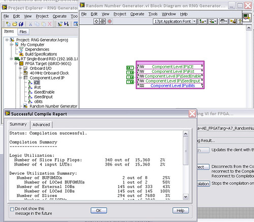
After that the output indicator comes with CLIP, compilation to fail...

NEITHER sbRIO-9601
LabVIEW 8.6.0
LabVIEW FPGA
Windows XP (32-bit, English)
No conflicting background process (not Google desktop, etc.).Usually a "trimming" error gives to think that there are a few missing IP. Often, a CLIP source file is missing or the path specified in the XML file is incorrect.
In your case I believe that there is an error in the XML declaration:
1.0
RandomNumberGenerator
urng_n11213_w36dp_t4_p89.vhd
fifo2.vhd
This indicates LV FPGA to expect a higher level entity called "RandomNumberGenerator" defined in one of two VHDL files. However, I couldn't see this entity in one of two files. If urng_n11213_w36dp_t4_p89 is the top-level entity, edit the XML to instead set the HDLName tag as follows:
urng_n11213_w36dp_t4_p89 Also - in your XML, you set the 'oBits' music VIDEO for output as a U32, however the VHDL port is defined as a vector of bits 89:
oBits: out std_logic_vector (89-1 downto 0)
These definitions must match and the maximum size of the vector CLIP IO is 32, so you have to break your oBits in three exits U32 output. I have added the ports and changed your logic of assignment as follows:
oBits1(31 downto 0)<= srcs(31="" downto="">
oBits2(31 downto 0)<= srcs(63="" downto="">
oBits3(31 downto 0)<= "0000000"="" &="" srcs(88="" downto="">Both of these changes resulted in a successful compilation.
Note: The only compiler errors when you add the flag because otherwise your CUTTING code is optimized design. If the IP is instantiated in a design, but nothing is connected to its output, it consumes all logic? Most of the time the FPGA compiler is smart enough to get it out.

Maybe you are looking for
-
Version 25.0.1 when I close the browser, all my previous tabs have disappeared when I open it again and it goes to the home page of firefox. I have my options set to reopen the previous tabs and I reset it at least 10 times and he won't stay. When I
-
Download photos on a Web site without export to desktop
I wonder if there is a way to select the photos in the Photos app on a Web site directly without first having to export them to another location. Example: On Facebook, if I want to share a photo of a friend profile, is there a way to select a photo i
-
PCI-1422 and RS 232 control of a camera Hamamatsu ORCA-HR (HR C4742-95-12)
Hello I'll have some incompatible problems when I try to control a camera Orca-HR (Hamamatsu C4742-95-12 HR) via RS232. I have a feeling that the problem comes from how the RS232 port emmbedded (emulated?) in the PCI-1422 is used or recognized by the
-
How do copy you & paste between email & browser. Or URL messaging or any way you want to go. It's IMPOSSIBLE. It was SO easy on the Bold 9900. To do a simple buttons copy & paste. Things that have been so easy on the "BOLD" are impossible on this z1
-
I ordered the 7 Home Premium to Professional Upgrade when I ordered my new HP computer, I picked up today. (for which I paid $65,00)It also suggested me the upgrade of Windows 8 when it comes out @ 15.00.If I lose all the benefits of the first upgrad