Duration of the impulse in labview FPGA
Dear
can help build a FPGA lv to measure the duration of the pulse
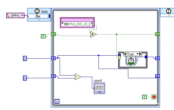
My first lv VI is illustrated below for Spartan 3rd kit the but its fail to work
Michel thei change operate?
for the case of structure in case of false the old value is moved instead of tick counter
Best regards
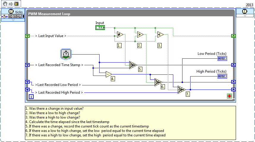
It is also an example in the finder NOR example on exactly how to proceed
You can search pulse to find it, or use the snippet below:
Tags: NI Software
Similar Questions
-
Please help me for this problem "error starting compile step: make sure that a compatible version of Xilinx tools is installed in the location specified in the setup of LabVIEW FPGA.»
Look for the error on the Web site of or or on the forums. Take a look at the following links:
http://forums.NI.com/NI/board/message?board.ID=170&message.ID=381394&requireLogin=false
http://forums.NI.com/NI/board/message?board.ID=170&message.ID=205754&requireLogin=false
-
How to use bidirectional I/O in the CLIP of LabVIEW FPGA?
How to use or define two-way i/o for CLIP with LabVIEW FPGA? I want to use 1-wire communication inside the kernel CLIP, the function will be implemented to read and write as I/O inside the CLAMP.
The XML Generator (CXG) 1.1.0 ELEMENT does not support.
Thank you
Supawat
Work after separate IB pin (bidirectional) at the entrance and exit. Thank you.
-
LabVIEW FPGA: An internal software error in the LabVIEW FPGA Module has Unknown
Sir/Madam,
Note Labview 2012 SP1 installed about 2 weeks ago.,.
Accident occurred during the compilation of an fpga vi who worked satisfactorally in the past.
When I restarted and went to the message recomplile "LabVIEW FPGA: an internal software error in the LabVIEW FPGA Module" see attached picture of popup.
I reinstalled Labview in its entirety and backed out the changes I made to the vi but still get the same message.
Thanks in advance
Daryl
It turns out that the question was in the VI and not of LabView FPGA module as the message may indicate. I created a vacuum vi, cut and pasted items in this from the vi error and recompiled and it ran very well.
Somehow the vi has been corrupted internally.
Thank you it's fixed.
-
Drivers Xilinx/Multisim and Labview FPGA
Where can I find drivers for my FPGA OR if I use Multisim/Xilinx and NOT of Labview? All the links I found are Labview be installed. However, the explicit manual FPGA indicates that you can use Multisim/XIlinx ISE in place.
OK, I tested just outside. The Driver of LabVIEW 2013 DEFB contains 2 separate components, the driver and Module FPGA support. If you run this installer, it won't check if you have LabVIEW FPGA installed unless you check the box for LabVIEW FPGA support.
I can change the text in the Installation Instructions to read "LabVIEW FPGA 2013 is required to install the LabVIEW FPGA Module Support component installation".
-
The President complied,
Is LabVIEW FPGA support for numbered kit ML-505 (Type FPGA: Virtex 5 LX110T) available or not? If Yes, where is it?
The only FPGA that is supported by LabVIEW FPGA is included in National Instruments hardware. You can't target the other with LabVIEW FPGA kits.
-
LabVIEW FPGA failure with compiler Xlinx?
I'm in LabVIEW FPGA 8.6 with NOR-RIO 3.0.1 (to 8.6). When I compile a simple program, I get the notorious:
«Error starting compile step: make sure that a compatible version of Xilinx tools is installed in the location specified in the setup of LabVIEW FPGA.»
I checked the FPGA compile server and I ran the utility fixTlink.VI with no improvement. This produces two identical PC, neither one having a FPGA installed card.
Any ideas?
After further analysis, the problem was to be in our facility in LabVIEW FPGA 8.6. Using the correct Installer of NEITHER solved the problem.
This thread is now resolved.
-
Integration of IP node evil in LabVIEW FPGA
Hi all
I am having trouble with the integration of LabVIEW FPGA IP option and was hoping someone could shed some light here.
I use a simple VHDL code for a bit, 2: 1 MUX in order to familiarize themselves with the integration of IP for the LabVIEW FPGA.
In the IP properties of the context node, the syntax checking integration says:
ERROR: HDLParsers:813 - "C:/NIFPGA/iptemp/ipin482231194540D2B0CC68A8AF0F43AAED/TwoToOneOneBitMux.vhd", line 15. Enumerated value U is absent from the selection.
but I'm still able to compile. Once the node is made and connected, I get the arrow to run the VI but when I do, I get a build errors in Code Pop up that says:
The selected object is only supported inside the single-cycle Timed loop.
Place a single cycle timed loop around the object.
The selected object in question is my IP integration node.
I add a loop timed to the node, but even if I am able to run the VI, it nothing happens. the output does not illuminate regardless of the configuration.
I would say that I tried everything, but I can't imagine would be the problem might be at this point given that everything compiles and the code is so simple.
I have attached the VI both VHDL code. Please let me know if any problems occur following different boards of the FPGA.
Would be really grateful for the help,
Yusif Nurizade
Hey, Yusif,.
Looks that you enter in the loop timed Cycle and never, leave while the indicator of Output never actually is updated. Try a real constant of wiring to the break of the SCTL condition. Otherwise, you could spend all controls/indicators inside the SCTL and get rid of the outside while loop. You can race in the calendar of meeting bad in larger designs without pipeling or by optimizing the code if you take this approach, however.
-
CPU register accessible in LabView FPGA FlexRIO
Hello people, I wonder if it is possible to get the following behaviors of Labview. I think that it is not.
Description of the system: application of CVI which communicates with SMU FlexRIO via controls and indicators.
Problem: The design of a CPU-FPGA interface specification which lists the "books" as a combination of reading and reading/writing-the bit fields.
Example:
According to the specification, there should be a 32-bit register. 31: 16 bits are read-only, and 15:0 bits are read/write, from the perspective of the CPU. In the world of labview, I would just do a uint16 control and indicator of uint16 and do with it.
However, to meet the specification (written for microprocessor buses) traditional, a reading of 32 bits of an address should read back the full content of the 32-bitregister to this place (implemented as flops on the FPGA, with appropriate memory within the FPGA device mapping). In the same way a 32 bits of an address entry must store the values in this registry (properly masking wrote at 31: 16 bits within the FPGA device).
Is it possible for me to have a unique address (basically, a component unique labview block diagram) that will allow me to accomplish this behavior? It seems to me that the only solution is to pack my records with bit fields that are all read, or all the read-write in order to register in the paradigm of labview. This means that the spec should go back and be re-written and approved again.
Thanks in advance,
-J
Thanks for the detailed explanation. I am familiar with the reading and writing in the FPGA registers - I did a lot of work non-LabVIEW recently with an Altera FPGA. I haven't, however, used the CVI to LabVIEW FPGA interface, I only used the LabVIEW interface. I'm not sure if your question is about the CVI, LabVIEW FPGA interface or both.
JJMontante wrote:
Thus, a restatement of my original question: y at - it a mechanism with the use of indicators of controls where both the FPGA AND the CPU can write to the same series of flip-flops in the FPGA? If I use an indicator, the FPGA can write to the indicator, but the CPU cannot. If I use a control, the CPU can write in the control, but can't the FPGA. Is this correct?
On LabVIEW FPGA, a control and indicator are essentially identical. You can write a check, or read a battery / battery, using a local variable in the FPGA code. It is common to use a single piece of front panel to transfer the data in either sense, and it's okay if it's a command or an indicator. For example, a common strategy uses a Boolean façade element for handshake. The CPU writes a value to a numeric control, and then sets the value Boolean true to indicate that the new data is available. FPGA reads this numerical value, and then sets the Boolean false, which indicates the processor that the value has been read. The LabVIEW FPGA interface (side CPU) covers also all elements of frontage on the same FPGA whether orders or the lights--they can be as well read and written.
That answer your question at all?
-
Simulate the sine wave using LabVIEW FPGA with NOR-myRIO and display in real time
Hello
I'm relatively new to LabVIEW FPGA. I am trying to test (and later apply) controllers high speed on myRIO.
At this point, I'm trying to simulate the sine wave from 1 to 10 kHz using Sinewave generator VI express. I also intend to display the sine wave on the time real (RT) using FIFO. However, I had a bit of trouble to understaing various synchronization parameters.
1. how to encode information about the sampling frequency generating sine wave? (The side FPGA vi requires only the frequency of the signal and possibly phase and does not rate update lines)
2. how to estimate the number of items in a FIFO? (that is, the relationship between the rate of updates to loop (RT), the signal frequency, sampling frequency and the number of items in the FIFO)
It would be great if we could share a very simple program (side host and target) that did something similar.
Thank you
MILIN
Milot,
I think the problem is the type of data in your FIFO. Your FIFO is configured to use a data type of I16. The problem is the number, it displays only ever will be-1, 0 or 1. To resolve this problem, you must send the sine wave as a fixed point data and convert it to a double on the side of the RT. This should significantly improve your resolution.
-
How to measure the frequency of sampling (s/s) in LabView FPGA?
Hello
I am trying to find a way to measure the sampling frequency (s/s) during which I read from analog input in LabVIEW FPGA. I know that the sampling frequency is specified in the data sheet of the module HAVE, but I want to measure in LabVIEW.
Any suggestions?
A screenshot of the example code would be greatly appreciated
Hey phg,.
If you have some time loopand in this loop, you export a sample by iteration of loop via an I/O node. You can't out two samples on the same I/O node within an iteration, it's always one!
So if your loop takes 1 second to run you have a sampling rate of 1 Hz output. The same goes for sampling of entry. How long your loop takes to run can be calculated as explained above.
Samplerate [s / s] = 1 / [s] while loop
-
If the butterworth filter available in LabVIEW FPGA is cascade, can I get a higher order filter?
I need a 10th order filter lowpass butterworth with cut-off frequency 5 kHz. Can I build by 4th cascading of 2 order butterworth filters and 1 2nd order available in LabVIEW FPGA each filter in butterworth with cut-off frequency 5 kHz?
This will increase the amount that your data will be filtered but will not increase the order in the Manor that you think. If you cascade two 2 4th order filters and compare that results to a filter of order 8, the resulting field filter cascading bode would look more like a 6,5e order filter.
Logan H
-
Compilation of the variable results in LabVIEW FPGA
Hello. I would ask why LabVIEW FPGA generates different results of compilation for the same code. When I compile several times my code, the maximum speed and total changes bitfile slices generated according to the compilation, but I does not alter with the FPGA VI. In addition, is the precise relationship of compilation? Thank you
It's normal. The FPGA compiler starts to place pieces of code on the FPGA somewhat randomly and adjusts them until either the design adapts and responds to the criteria of the moment or there that the compiler determines that it cannot fit all the code and meet time constraints. The outputs that the FPGA VI generates when run will always be the same.
-
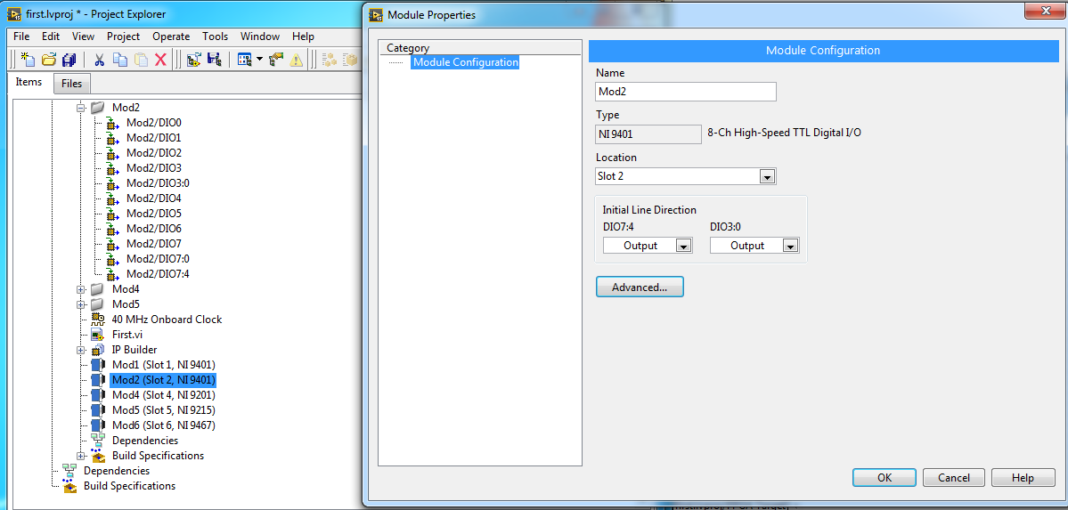
Configuration of the inputs/outputs of NI9401 in labview FPGA
Hello
I am very new to Labview FPGA. In fact, I'm implementing the very first example introduced by OR for learning Labview FPGA. I need to connect an entry of a NI9401 on one exit from the other.
However, when I drag and drop the input/output units, the two act as inputs:
I also changed the propties one of the NI9401 to act as output. But the problem persists.
It is the example that I am building.
I'd appreciate any suggestions.
https://www.YouTube.com/watch?v=mv112V-P030&index=1&list=PLbCk9hRe-ziECXQjE--fN29C_kcx7CHnA
Right-click on the output node, and then select "change to write."
-
problems with the project of example LabVIEW FPGA
I'm trying to adapt the example project record on CompactRIO and LabVIEW FPGA Waveform Acquisition for my hardware, but can't seem to do things. I'm just following the instructions in the tutorial, but can not make sense out of section adapt this example to your hardware project, in particular, the instruction to "Drag FPGA Main.vi in the Project Explorer in the Open FPGA VI service window reference VI." Can someone explain on what is supposed to happen here? BTW, the target hardware that I'm doing this work on is a cRIO-9068 with some C series i/o modules.
Finally, I came across the answer. For anyone else who may encounter this problem, the attached screenshot is worth a thousand words.
Maybe you are looking for
-
My Mac has a vertical line on my screen, up and down, about 1/3 left. The line is very small but clearly visible. Any solution? Thank you.
-
Error message incorrect file size when the BIOS update on Satellite M100
When you try to install the BIOS update I get the error message: incorrect size of the ROM file. What can I do? Thank you.
-
Satellte P750 - constantly overheating
Hello there :) My PSAY3A Satellite - 15 d - 3 K P750 (bought late April this year) has been overheating quite often lately.Initially it was not a problem but for the last month or two, has been overheating on almost on a daily basis. I bought one of
-
Need for information of the motherboard of Equium A60
HelloI'm trying to find out about my motherboard, I an Equium A60-155 , and I was wondering if someone could help me
-
How to crack open a Sandisk flash drive
I was just curious to know if anyone knows of a module fail-safe way to crack open the plastic packaging of these flash drives. It does not matter I've got 4 GB, 8 GB, 16 GB and 32 GB models. If you can show me how to open one of them I should be abl