Implementation of I2C in FPGA on SOM devkit
Dear all,
I have this sbRIO 9651 SOM with jury of carrier of reference with which I would like to connect a sensor of MPU 6050 Pmod 5 and acquire sensor data in an FPGA VI and process data in a RT VI. I find it difficult to implement I2C interfacing to FPGA as I am relatively new to FPGA programming in LabVIEW. MyRIO implementation was pretty easy as the API and usage example it was easy to access. Any help would be appreciated.
Concerning
Guenoun
Hello
I found this documentation to be very helpful:
https://decibel.NI.com/content/docs/doc-41410
She described the meaning of in, out and activate. SCL clock series, SDA is given in series. In and out are to read and write data, activate switches between being an input or output pin. It is what explains the wiring in this post on the forum: https://decibel.ni.com/content/message/127591#127591
The I2C bus is high when idle, so out is set to false (bass), but this has no effect because enable is false. In order to drive the bus low, enable is set to true. Now has an effect and driving the bus low. If the bottom of the bus is set to true to activate while the output is held low literacy.
I hope this helps you.
Alex
Tags: NI Software
Similar Questions
-
try to implement jQuery clock and I have some doubts...
First of all should I install the jquery library in apex 4...
I thought that the library jquery already present in the apex 4...
What are the new features of jquery in apex 4... I am comparing it with apex 3...
I thought that jquery is integrated in the apex 4...
See the example in the following link
http://Apex-notes.blogspot.in/2008/11/timepicker-and-apex.html
I did everything mentioned above... the link above apex-notes...
But I can't seem to get the time clock...
Do not know where this part of the code should be added... It's the last activiity mentioned in the above link... http://Apex-notes.blogspot.in/2008/11/timepicker-and-apex.html
script type = "text/javascript" >
{$(document) .ready (function ()}
cback function (time) {}
var c is $("< div style =' couleur: rouge" > heure d'entrée: "+ temps +" </div > ");.
c
. Hide()
.insertAfter (this)
.fadeIn (1000)
.fadeOut (1000);
}
$("#P9_TIME").unbind (.clockpick({))
StartHour: 8,
EndHour: 20,
({showminutes: true}, cback);
});
< /script >
Published by: susf on 19 June 2012 02:35Why all expect you a clock? It won't show a Visual clock just because javascript library name is clock.
First of all know what he does and then put implementation.
Learn jQuery and try some of these plugins
http://www.ajaxupdates.com/jclock-jQuery-clock-plugin/
http://joaquinnunez.CL/jQuery-clock-plugin/
http://www.Google.co.UK/search?AQ=0&OQ=jQuery+clock+&sugexp=chrome, mod = 0 & sourceid = chrome & ie = UTF - 8 & q = jquery + clock + plugin
-
I2C implementation using NOR-6008
Hello world
I have a NOR-6008 low cost multifunction data acquisition.
Can I use this with shifter voltage level to apply the I2C Protocol...
You must use the approach of bit - strike (i.e., change you the clock and data lines yourself) and it would be timed by the software. But yes, you could do.
Your next question will be: are there examples? There are many examples on the conduct of IO digital who settle with DAQmx. Regarding the implementation of I2C, the spec is available. http://en.Wikipedia.org/wiki/I%C2%B2C
-
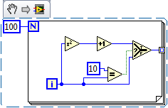
case of structure on a FPGA implementation
Have been programming in BT for many years, I am new to FPGA. In the following code, the method of bottom should normally be the right method; only the execution of the equation once instead of each iteration (100 X). But I was told that on a FPGA, two cases of the case structure run each iteration with the used appropriate output (can you please confirm or refute this?) If this is true there is essentially no difference?
If this is true, is there a place any with a machine to States on a FPGA or all code must be written "dish"?
Thanks for your help-
lmd2
Imd2,
It is true that on each itteration the FPGA will calculate the results of these two cases. This is because the circuit is implemented in hardware parallel paths in order to not necessarily slow down execution. If you use the select block as in the example below, more it shows directly how this will be implemented on the target FPGA hardware.
Furthur to optimize this code you can perform a single-cycle timed loop inside the loop for MAX so your speed.
Hunter
Supporter of LabVIEW FPGA
-
Hi guys,.
I use a SBRIO-9611 to control a few shavings DAC using I2C. I did some research and found the link below.
Unfortunately, I'm using 8.5.1 both for my FPGA software and in real time. I need a kind soul help me downgrade 8.5.1 code so I can open it.
Thank you
Ray
https://decibel.NI.com/content/docs/doc-1151
Hi Ray,
Here is the converted project

Concerning
-
FPGA - windowed moving average, variance, standard deviation, kurtosis and asymmetry
Hello!
I'm processing in FPGA and I want to calculate the MOVING WINDOW average, variance, standard deviation, kurtosis, asymmetry online for the last N (N is the size of windows) elements. The frequency is about 100 kHz and N about 10000 (100 ms of signal).
I found something like EMA (moving average exponential)...
Have someone solved something like that? Any ideas how to fix?
That looks like a problem. What type of window you need? The moving average exponential isn't an option? There are online algorithms described in Wikipedia, but they can suffer from problems of numerical accuracy when it is implemented in a fixed point (depending on the nature of the data). They would be interesting watch in, however.
Other than that, here are some options that I can think of:
- More large FPGA
- Be part of the treatment on the RT controller - have - you looked into that?
- Return to your needs and push some of the numbers. Do you really need 100 ms in all cases, etc.?
- Depending on the nature of the data, simple compression techniques may be an option
- An precision analysis to determine the data type minimum, that you really need. For example, getting to 25 bits, would have a huge impact on your cost of multiplier.
- Consider the mathematics of floating (using Xilinx IP cores) point to online methods. Your flow is relatively low, so you could share it resources between all channels. Manage States of different channels is complicated but is doable.
The BRAM will be used for FIFO buffers, but is also available for general use to implement the fifo and memories. Some IP use BRAM under the hood, keep an eye on the compilation summaries to monitor how much still you have.
-
I am trying to stream as quickly as possible from the to a FlexRIO 7966 5154 digitizer. From the example "NISCOPE fetch Forever" in LV2012, I can implement the acquisition on 5154 @ 40MS/s, 50 k of data I8 piece and the graphical indicator seems to keep well indefinitely.
I tried then write data to an FPGA - FIFO target host, and it chokes. With FIFO write the method inside the loop of 5154 fetch the 5154 ends in error because of the "overwhelming memory" (it fills its on-board memory until the HOST is reading). With FIFO writing in a parallel consumer (queue conduit) loop, the queue overflows just because he can't write that as fast as the 5154 FIFO provides samples in the queue. What Miss me? The 5154 uses a PCI DMA bus (I think), so I think that if he could hold, the host to the FPGA PCIe bus must be capable.
There is another factor, that I have not taken into account? Sorry I can't provide the VI since the installation of the LV is on a PC not connected to the network. Any advice or suggestions would be appreciated.
Thank you
Mark Taylor
For future reference, I ended up resolving this by moving the implementation on the actual FPGA. I had run in mode "on the development computer with i/o simulated" and no matter what I did with the start-up or sizing FIFO sequence, it just doesn't work.
After compiling and running on the FPGA, all right. Maybe it's the basic knowledge, in fact I remember somewhere in my travels reading that don't accurately represent timing problems when running to the old fashion, but LV FPGA has kind of us painted into a corner with the compromise of simulation/compilation. They do not include Modelsim, which is the only tool that enables co-simulation do functional and verification of the timing set (we Questa, unfortunately) and independent VHDL simulation captures the interaction host with precision (and software processing/timing is impossible to quantify!). In my situation, the only way to operate at speed is in the FPGA, but then I can't see all of the things that I need to see to debug... ARGH!
Additional links and resources always will welcome (on debugging of FPGA LV and design in general). I found a couple of things below, which was somewhat useful:
"NEITHER powerful LabVIEW FPGA Developer's Guide"
http://www.NI.com/Tutorial/14600/en/
I found a link to an "FPGA Debug Reference Library": http://www.ni.com/example/31067/en/, but my installation does not seem to have this available.
And it looks like 2013 may add functionality to help alleviate some of this via the node of the execution of office referred here to the 'Test and debug LabVIEW FPGA Code'
-
Violation of timing when adding code blocks parallel to each other in a FPGA SCTL
Hey guys!
I have a problem with my code inside a SCTL of running on an FPGA VI and hoped someone could help me.
I work with a 120 MS/s ADC and write the data to the FPGA block of memory in a 120 MHz SCTL. Since the data has to be 'mixed' there is also a code to get the correct address (by first example data at address 0, second to address 20, 40 and so on until 2000, then I start with 1, 21...).
I have a second block of code that later, when writing is completed, reads in the block of memory to perform some calculations (a linear slope of the signal interpolation)
The two parties are implemented using pipelining (I say this because I think it would be the first response of the community), while if I compile only one, everyone needs about 7 to 8 ns to run, which means that they meet the requirements to run in my 120 MHz SCTL (8.33 ns).
But when two blocks of code are in the same field of clock (whether in ore SCTL in two SCTLs using the same clock) from the FPGA VI I get a timing violation, saying that the code in the SCTL needs 17 ns (logical and delay routing) to run. It is not also show me the critcal way, just the SCTL. Because the code runs at the same time, I don't see why the delay of logic should increase (to 12 ns). The only way 2 code blocks communicate with each other are the memory of block and some shift registers so the path of Combinatorics is not increased.
I already checked whether the SubVIs (I use one per block of code to avoid the lack of clarity, but they are different) are the problem. If the code in the SubVIs implemented directly in the FPGA hand VI it does not change the delay of logic.
50% of the registers and the lut FPGA are used, the DSP48s of 5% and 50% of RAM block, so I don't think that the problem is something like the compiler finds not enough free slices to create fast paths.
The main problem is not that the delay of routing increases, but the delay of logic.
Does anyone have an idea what could cause this huge increase by delay time?
I use labview 2011 and 12.4 Xilinx.
Try not to put memory read the node within a box structure. Instead, you can always read from a fixed address, say 0, when the data are not all ready. Reading a memory will not damage your data contrary to push from a FIFO. If your memory by reading the node is inside a case structure, there will be a mux when data is passed outside this business structure, which will increase the delay of logic.
In addition, I also recommend that you do not use the loop of the index 'i', if you are running at high clock frequency. This counter is seen to be 32-bit, and you probably don't have a memory that deeply. LV FPGA is to have logic check inside the read node memory address range, so width incorrect address can still be important. You can implement instead of your counter code which the width of the tip is appropriate.
-
Dear all,
Greetings
I need assistance to implement an I2C protcol in sbRIO 9636 (KIT of RIO could), I try one of this website (http://zone.ni.com/devzone/cda/epd/p/id/4063) after moving to screw for my kit and deploy it I couldn't have expected results, as shown in figure (start condition) instead, I got the figure of output (output). any suggestion? Help, please...
Thanks in advance
Mustafa
-
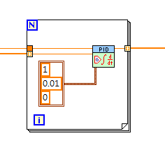
How to implement multiple tasks (e.g., PID) in parallel?
Hello
I know there must be some questions like this in this forum, and I tried to find for a while but got some what I want. My project is a little urgent that I post this question for a few instant suggestions...
As the topic says, I have several devices, say energy suppliers, and I must adjust their power automatically and independently.
Although the number of devices is eight for the moment, but I prefer not to fix the number, otherwise said, I want to scale or increase the number of device dynamically.
As a first step, I am very stupid to put the PID.vi in the loop for...
I was wondering if the activation of parallelism can deal with my problem, but soon, I knew that each appellant VI data spaces are mixed upward...
I'm stuck on how to book space for reentrant data...
The last one on my mind is the VI open to the outside at the beginning of the control and take advantage of VI references...
But I have not implemented the method, there may be some other thorny issue on this way...
Is there a way to sovle this kind of problem?
Hi William,.
PID functions support several control loops, just read the Help for functions!
No need for this loop FOR (which is simply wrong here)!
-
Matrix inversion complex on FPGA
Hello
I implement a simple code on SMU-7966R. I need a function that calculates the inversion of a complex matrix (fixed-point). I was wondering if there is an existing library that provides the service or I must apply myself.
Please can someone enlighten me?
Thank you.
I don't quite know librares for the execution of complex matrix inversion.
There are two ways I used for the development of own implenetations. Both methods involve the decomposition of the matrix A through rotation matricies.
(1) the QR decomposition through Givens rotations where is QR. This method breaks down the matrix in a unitary matrix Q and a upper triangular matrix R. The inverse of Q is simply its transposed to Hermetian because it is unitary. The inverse of R can be solved for by back substitution. Multiplying the inverse of Q and R gives the inverse of a.
(2) use the signular A value decompositon to get two unit matricies u and V and a diagonal matrix S of the signular components. Again, reversing the unitary matricies is simply the transposed to Hermetian. The inverse of the diagonal nmatrix is only taking the reciprocal of the diagonal elements. The SWINE vesicular disease can be performed using an algorithm called the cyclic Jacobi method. This method is slightly more complicated than the QR decomposition since it requires an additional rotation matrix, but it avoids the back problems through substition.
These two processes are iterative and converge to the exact solution as the number if iterations increases. While math can seem a little daunting at first, there is a lot of literature on these topics including different FPGA implementations. Just google 'FPGA QR Décomposition' or 'Method of FPGA Jacobi'.
-
Effective use of the FPGA read/write
I am writing an application for a CompactRIO real-time and I am looking for ways to simplify my code and reduce the CPU usage. I use FPGA to do much CAN e-mail and signal processing, then I have a VI running on the real-time processor that reads values in the FPGA, does some processing and outputs data in the FPGA. My code running on real-time parallel uses several loops running in a master/slave architecture. A single loop reads all necessary information in the FPGA in indicators and writes the values of the controls in the FPGA. The other loops read entries and manipulate the outputs via local variables.
My question if it would be more effective to get rid of the loop which is dedicated to the communication of FPGA and has of each loop to read and write directly on the FPGA. If I use a reference block FPGA open and use the reference of the output in several loops, each read/write operation block others until it's over? Each output is changed only in one place in the code, but there are several entries that are used by multiple loops. It is even more effective for each loop of read/write for the FPGA on request? How will this affect determinism?
Thank you
Jon
Jon,
Read/write controls is not deterministic, but I think that your previous method should work just fine, as long as you have that unique writers. If you have multiple writers, you start affected by race conditions.
I don't think you will see a significant improvement in the performance/CPU in the alternative method. You would see big performance gains if your master loop reads more slowly indeed, but it's always a compromise.
-
Error FPGA - object internally in pipeline not connected to the sufficient number of nodes comments
Hi all
I'm currently implementing LMS on module FPGA of myRIO 1900. I couldn't fully understand the following error.
"Reading memory: internal pipeline object not connected to the sufficient number of nodes feedback"
Details:
"The selected object has a built-in shift register that makes the output on a particular loop iteration correspond to the entries in the previous iteration.
Connect the outputs of the object directly to a minimum number of nodes of Feedback or uninitialized shift registers. You cannot connect the outputs to another object. "
I just tried to access the values of two briefs and add them. The address for two memory values are the same, but the memories are different. I tried to implement this on SCTL, it doesn't but on normal everything in a loop, it works.
Help me understand the error.
Thank you.
Post an excerpt of your code would help us to be more confident, but I think that you run in the error described in the second note of this help documentation.
http://zone.NI.com/reference/en-XX/help/371599L-01/lvfpgaconcepts/fpga_memory_items/
Using the parameters of memory default point that you have to attach a feedback with a x 2 node latency on the release of reading to use within a single cycle timed loop.
-
Camera Basler ace not yet implemented?
Hey guys!
I use the new Basler Ace acA1300-30gc. I have installed the latest device drivers and Vision Builder 2009 (I have them on a seminar OR a week ago). When I opened the pylon Viewer camera works fine, but when I try to run the program in the Explorer of measurement and automation it is, but it does not display the image. I get this error:
The IMAQ error
0xBF69008
Not yet implementedIs - it may be that NEITHER device drivers do not yet support the new camera? It's actually 6 months, so I think that there should be a solution already. Help, please.
Thank you!
Matej
Matej salvation,
I believe the only reason why you get this error message (sorry, it is not more descriptive) is because the Pixel Format image you have selected is not implemented by IMAQdx. I think some of the Ace color cameras have a specific format of YUV color that are not supported. You should be able to move from a Bayer or another YUV format, save it in measurement and Automation Explorer and turned off the acquisition.
Eric
-
Implementation of Oracle Business Intelligence Applications
As a consulting company, how many type of resources, we must implement the Oracle Business Intelligence Applications.
For example, we are going to implement Business Intelligence for Oracle Financials R12.1.3 and Oracle HRMS R12.1.3 then what type of resources, we need?
According to my believe according to the types of resources should be involved.
1 database administrators (in order to exploit the security things facility)
2 BI Technical Consultant (Oracle Financials, HRMS with OBIA map)
3 BI Consultant (to explain the dashboard in front of the customer knowing the field)
4 project Manager (to administer the process of implementation)
Please delete my agreement with some suggestions.
Thank you
Naeem AkhtarHi Naeem,
You must have technical / functional Oracle Financials R12.1.3 and Oracle HRMS R12.1.3 Consultant if you want to customize finance OBIA or OBIA HR. These consultants will help you:
-analysis of the DIFFERENCES between the content of OLIVE & operational requirements
-understanding customization in EBS module to adapt OBIA
-understand the source tables and between the source tables to customize OBIA.Kind regards
Benoit
Maybe you are looking for
-
I have a business Web site www.rove-n-ramble.com , it works fine in ie and chrome. But not in firefox (38.0.5). The main problem is in the part of cursor. The cursor almost out of the page instead of in the middle and so ugly. PL. help me in this reg
-
P40-10 X Equuim: Reception of WLan is very good, but extremely slow
Hello I just bought an Equuim P40 - when I connect to wireless broadband, the reception is very good but is extremely slow when it comes to load the pages of the internet - any suggestions on how to remedy this?Thank you!
-
Screen LED-2311 x - idle time return to the screen of the monitor
Hello the only problem I'm having is that when my computer shuts the screen due to idle time, when I move the mouse to wake up, the monitor will be taken more than 10 seconds to display the... I got more than 5 monitors, all display the screen in 5 s
-
Correlation coefficient vi Labview 2013 for two tables 1 d of zero, r values is NaN.I don't know why?
-
643 and 646 error codes when tried to install extract
Original title: security updates for Vista and MS Office I have 19 updates of security that will not be installed. Ten are for MS office 2003, 1 for MS Vista NET Framework 1.1 SP1, and 8 are for MS Office 2007. I keep getting error 646 and 643 codes.