LabVIEW synchronous clock
need help explaing this program, from what I see the frequency is being recorded and the data acquisition card is used.the frequency is converted to seconds, then the hours etc. mins/s for a clock display. struggling to understand the dome of things 'format string' etc. no matter which help to explain what the complete operation is here? Otherwise, no problem
for a synchronous clock, using the frequency of the supply voltage, clock being a screen seven Sergeant, 6 of them
Tags: NI Software
Similar Questions
-
I have a question about a FPGA project I'm developing.
I use a digital RIO NI PCI-7813R, objective and Module FPGA 8.6.1
I implement a SPI bus, master.
I use a state machine in a single loop of Timed Cycle. (about model on one of your examples IP)
I'm running the loop at 20 MHz, which produced a clock of 10 MHz SPI bus data.
I send you the data in 8-bit bytes delivered by a FIFO of the host.
Similarly, I return data bytes of 8 bits of the host by using a different FIFO.
I have no problem sending data, generate all the select chip and data impulses on my desired clock edges.
It's manual clean and perfect as seen on a scope / Logic Analyzer.When I read data from i/o pin however I have found unexplained behavior.
It is this: the data seem to be trolling by two read operations.
When I read the axis of I/O data to the specified limit of the clock that I generate.
I found that the data were two bits shifted to the right, i.e., deferred, one on the scope / Logic Analyzer.
I did a work around by two pins I/O multiple read operations in time of the gap between the data bytes.
There are no generated clock signal and no data valid on the I/O pin at the time of these two read operations as testified to by the scope.
And now the data received matches perfectly to the one sent.
I can only assume that there is some kind of pipeline or delay inherent in the IO read operations. (at higher clock rates)I suspect that there may be something in the optimization performed in the compilation of the structure of the SCTL the cause.
I had found it, sometime before in my development, that data has been little offset from 1 only one position.
I think it was at a slower pace of global clock.I also ran the same state machine in a classic logic expect everything in a loop with an FPGA, to produce a much slower system
and I found that there is no delay at all.I don't see anything in the configuration i/o pins that can affect this. (I turned off arbitration)
Similarly, I don't see anything in the documentation that could refer to this behavior.
8.6.1 of LabVIEW FPGA Module Known Issues (http://digital.ni.com/public.nsf/allkb/F6B5DAFBC1A8A22D8625752F00611AFF)I'm about to use and deploy the code with the solution because it seems to be reliable.
But I am at a loss to explain (in my documentation of the code) why it is necessary
or how to solve this problem if the compiler changes.
Do you have any suggestions?I think that what you run is that the number of sync records used with the digital I/o. If you right-click on the I/O item in the project and select the property page, you should see an option for number of registers for output and output enable synchronization. These settings are global settings for this I/O item that will be the effect on all nodes of the I/O writes to this point of I/O. Similarly, if you right click on the e/s on the schema node and select Properties, you should see a setting for number of registers of synchronization for playback. This setting is specific to this instance of the node for this element of I/O and can be configured differently for each node in the diagram. The effect is that each sychnronization registry will delay this beating of a clock signal. These records are inserted to prevent the problems of metastability and ensure that you always have signal levels valid when the IO is sampled on the edge of the clock. There is a problem whenever the producer and the consumer of the signal are market off different clocks, or at different clock rates. If the external device drive your digital inputs work synchronous clock you are producing, you can eliminate the registers of the synchronization. However, you must perform an analysis of delays in propagation of the signal between the two devices and make sure that all the settings and hold times are always met before. In the end, I think that the easiest and most robust solution will be to compensate for delays in sync in your code as you do already. I hope this helps clarify things.
-
According to the Manual (which is 6 years old) for IOTech DaqBoard 1000-series can only be used with a DaqBoard both Dasylab.
Is this true for the latest version of Dasylab?
It can, but especially this means that all boards must use the same sampling rate, or a rate of divided down.
The user guide says to drive improved:
The improved driver IOtech uses the standard/a. DASYLab driver interface, which traditionally has supported a
device of unique material, with optional channel expansion cards. The standard DASYLab driver IOtech is a
example of a single traditional support driver.The improved IOtech DASYLab driver supports conventional device applications within DASYLab as well.
In addition, holders of driving more acquire data from multiple synchronized clock devices via the
module analog input of DASYLab standard. The improved driver carries out this mission by creating a single large virtual
device inside DASYLab. Since all the input from the point of view software DASYLab channels are located on a single
virtual device, the data of all devices must be returned to DASYLab in a single stream. The IOtech
DASYLab drive and it supports DaqCOM driver layer manages data from multiple merging
devices in a data for DASYLab streams.This virtual device unique architecture of the forces from the point of view software DASYLab all channels to gain entry
data at the same sample rate. At the hardware level, devices can be designated as slave devices and acquire data to
even the clock divisions of the master clock frequency. IOtech drivers manage scans of padding of slow devices in data
buffer to create a uniform input data stream. -
Stupid question: enum to export to CSV?
I will be putting together a sizable statemachine, the State will be displayed on an HMI via ModbusTCP.
This has GUI to a 'View Message' tool that searches a string of text to display from an integer value.
I would like to avoid having to keep this display synchronized manually with a large enum typdef I will be constantly change, so I'm poking around in labview with typedef enum another, smaller, there is a way to get the list of items (like when you change items) hoping in excel, for cut-n-Paste in the GUI tool.
Do not see. Whatever this is built in?
I guess I could write something to run on my development computer... all done already - perhaps?
A list of items in a csv or text file or xls?
Or use "GetNumericInfo.vi" found in vi.lib\utility\VariantDataType. Wiring in an enum, out of an array of strings containing the names of enumeration. Has the advantage that it does not require access to the front and work on RT. I wrote once a little VI that it used to automatically generate a header file C that contain enumeration values to keep C and LabVIEW synchronized code.
-
Hyperic alert metric of availability
HelloI have a problem with Hyperic event alerts on availability.I just want to alert and e-mail when a server is no longer available. I use the metric standard of availability that Hyperic collects and the alert I set the triggers on the event that availability is equal to 0%. I am getting a lot of false positives where I'm alerted that availability is 0%, but when I look there is no problem on the analysis server, and even the chart availability shows no sign of 0% availability.I tried to configure the alert to trigger only when the 0% event occurs 20 times in 1 hour, but even this still falsely raise the alert sometimes. I tried this in different environments and exhibit the same problem everywhere.Is there an easier way to detect when a server went down or are no longer available?Thank you
Hello
I have a problem with Hyperic event alerts on availability.
I just want to alert and e-mail when a server is no longer available. I use the metric standard of availability that Hyperic collects and the alert I set the triggers on the event that availability is equal to 0%. I am getting a lot of false positives where I'm alerted that availability is 0%, but when I look there is no problem on the analysis server, and even the chart availability shows no sign of 0% availability.
check the time synchronization between the server and the agent.
Hyperic is very (IMHO too) sensitive to the poorly synchronized clocks, and false alarms on metrics of availability with no evidence of a failure on the server are the most common symptom.
-
Model a block synchronous dual-port RAM with LabVIEW FPGA
This question caught my attention recently.
I am trying to model a particular design element called "RAMB4_S8_S8" with the LabVIEW FPGA module. This element is a block synchronous dual-port RAM allowing simultaneous access to two ports independently from each other. That being said, a port can perform read/write operation to this RAM while at the same time, the other port might be able to do the same thing. There are two opportunities of possible port conflict, however. The first is when both ports are trying to write to the same memory cell. The other scenario is when a port writes in a cell memory while at the same time the other port reads from it. Other than that, everything should be a legitimate operation.
In order to reproduce this I select memory block that is integrated into my FPGA target. An interface is configured to be the playback mode, and the other is set to write fashion. For the option of arbitration, I let the two interfaces to be "arbitrate if several applicants only. Then I got a compiler error when I tried to run my FPGA code for this model in a SCTL. The error message is something like "several objects to request access to a resource through a resource configured with option interface" arbitrate if several applicants only ", which is supported only in the single-cycle Timed loop if there is only a single applicant by interface.
This error goes away if I replace the SCTL with a simple while loop, but not what I would like to implement. So I wonder if there is a better solution to this problem, or is it just the limitation of the LabVIEW FPGA module.
Thank you.
Yes, you can use a form of conduct to perform the operations you want in the generations clock cycles, but all the code is inside a single SCTL. Basically, read the first address and storing in a register in a single cycle and then read the second address in the second clock cycle. This would allow you to two readings of valid memory every clock cycle 2. I have included a crude extract to illustrate the concept. The case selectors are identical with address A being connected to the memory in the true case, B in the case of fake address. Your biggest model memory dual port will be intact, but it will operate at 1/2 rate.
Take a look at the white paper that provides more details on the construction of memory:
Data on a target FPGAS (FPGA Module)
The ball on the memory block indicates that memory block double port cannot be applied in a configuration of reading, which is a double ROM. access read/write port must be imitated with custom code.
-
Reference clock synchronization and clock of sampling (not LabView but Daqmx, Sync and C)
Well, I found an example that resemble what I wanted... in LabView: http://zone.ni.com/devzone/cda/tut/p/id/9308
Now the question is all about timing of the timestamps and sample:
Here is a list of ficelleStringString ficelleT of what I called...
DAQmxCreateTask
DAQmxCreateAIVoltageChan
DAQmxSetRefClkSrc (used NISYNC_VAL_CLK10 = "PXI_CLK10")
DAQmxRegisterEveryNSamplesEvent
niSync_init (used a PXI-6682)
niSync_SetAttributeViInt32 (used Terminal = NISYNC_VAL_PXISTAR0 and NISYNC_ATTR_1588_TIMESTAMP_BUF_SIZE = 3000)
niSync_CreateClock (used Terminal = NISYNC_VAL_PXISTAR0)
niSync_EnableTimeStampTrigger (used Terminal = NISYNC_VAL_PXISTAR0)
Now this list makes me able to create a timestamp every time the clock triggers a RISING edge...
Now how to synchronize these timestamps are useful for my sample? (I mean I need to sync my calendar with the PXI_CLK10 card) because for now prices will not match the sample rate.
ALSO... a little weird...
some of my cards will accept DAQmxSetRefClkSrc but others must use DAQmxSetMasterTimebaseSrc.
Now I can't use DAQmxSetMasterTimebaseSrc with PXI_CLK10... no idea why...
So, how did I would synchronize THESE cards...
Alright I could totally be wrogn with my approach, but I'm new with stuff of OR and using C isn't exactly the best documented piece of the NC.
Thanks in advance,
SEB
Thus,.
We have the same clock sampling for all of these devices, but we are not PLL'ing with the card of the S series, we cannot guarantee that they will all be in phase. However, given that all of these devices would be based on the same reference clock, we would not drift when we started the task. Would this work?
An alternative is to use the new X-Series card, which can also do a simultaneous sampling, but I don't know if it is feesible within your application.
-
Hello world
After 10 years of LabVIEW experience I'm totally lost.

It's my first project with DAQmx and I do not know how to handle.

My configuration: Windows7. LabVIEW 2012 DevSuite; X Series USB-6366
My goal: trigger value encoder and 2 inputs analog
I would get a result for the value of the encoder and each of the two analog inputs for each change of the value of the encoder (not more! I do not want to sort a huge amount of data afterwards)
I was able to configure it with the measurement and Automation Explorer, but have no idea how to do that in a LabVIEW configuration.
Read all of the examples I could find the analog inputs and the encoder with SampleClock. This isn't what I'm looking for.
I would be very happy if someone could guide me to my solution.
I have attached the confiuration exported from the measurement and Automation Explorer.
Thanks in advance, best regards,.
Balze
P.S.: Sorry I got COMPRESS the *.nce file, because NEITHER allows you to attach files *.nce

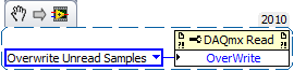
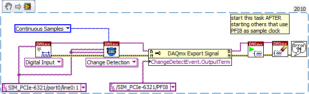
You'll get there, but yes, the first exhibition to DAQmx is probably a little overwhelming. A few other tips based on your screenshot (I'm on LV2010 & can't open the code).
1. "allow buffer overwrites" is that a functional but description is not text. It lies under the Read DAQmx property node and must be configured before starting the task. Here is an excerpt:
2. it is usually (but not always) an available timing system to be used for all HAVE channels in a task just by the material. As a result, all channels to HAVE should be included in a single task. You can do this easily in chaining your call 'DAQmx create Virtual Channel' twice the job output and input/output error. Because the second call will receive a task refnum as input, it will configure the 2nd channel of AI to be part of the same task.
(It is possible to specify just several channels in a single call, but separate calls gives you the ability to configure different setting on the scale or range of entry).
3. the 'random', which IA task gave you the error is due to the lack of sequencing in your attempts to start tasks. The question which is the fortunate success that happens to run first can (and does) vary from run to run. By combining the two channels to HAVE in a single task, this problem will disappear, but you want to be sure that the tasks of the AI and the counter are started * before * any clock signals come to PFI8.
4. "change detection" will be available for digital input assignments, not tasks of meter. And it is also generally supported only for a digital port a-bit value. Other ports then that support data acq clocked by the software on demand. I guess one of these questions is the source of your error.
On the boards of the M series that I used, change detection has been supported only on port 0 - I think that the same thing will be true for the X-series cards. The following took place without error for me using a simulated X series device. By selecting another port gave an error.
-
labview real-time clock display
Hey dude, im doing a project on labview that I just want to make prettier for the speaker
is it possible to add a clock to the façade that tell time, ideally in format:
any help welcome
Thank you
Kevin

Pretty cool Tim. Here is an old floating around, I got that has a neat wooden face and the code is really simple. It is in LV10.
-
LabVIEW FPGA: Integration node clock wrong
Hello
I'm having some difficulties to understand how the clock is part of the node IP for LabVIEW FPGA and was hoping to get some advice.
What I try to do is to set up a digital logic circuit with a MUX feeding a parallel 8-bit shift register. I created the schema for this Xilinx ISE 12.4, put in place and can't seem to import the HDL code into an intellectual property node. When I run the VI, I am able to choose between the two entries for the MUX, load the output in the shift register, clearly the shift register and activate the CE.
My problem is that when I switch to the entrance of THIS, he should start 1 sec shift (Boolean true, SCR, High, what-have-you) in the registry once each clock period. Unfortunately, it instantly makes all 8 bits 1 s. I suspect it's a question of clock and here are some of the things I've tried:
-Specify the input clock while going through the process of configuring IP nodes.
-Adding an FPGA clock Constant as the timed loop.
-Remove the timed loop and just specifying the clock input (I'm not able to run the VI that I get an error that calls for a timed loop)
-Do not specify the clock to enter the Configuration of the IP node and wiring of the FPGA clock Constant to the clock input (I can't because the entry is generated as a Boolean).
-Remove an earlier version of the EC who had two entries up to a door and at ISE.
-Specify the CE in the process Configuration of the IP nodes.
-Not specify this in the process of setting up nodes IP and wiring it sperately.
-Various reconfigurations of the same thing that I don't remember.
I think I'm doing something wrong with the clock, and that's the problem I have. Previously, when I asked questions to the Board of Directors on the importation of ISE code in LabVIEW FPGA, a clock signal is not necessary and they advised me to just use a timed loop. Now, I need to use it but am unable to find an explanation online, as it is a node of intellectual property.
Any advice would be greatly appreciated, I'm working on a project that will require an understanding how to operate clocks the crux of intellectual property.
Thanks in advance,
Yusif Nurizade
P.S. I have attached my schematic ISE and the LabVIEW project with one of the incarnations of the VI. The site allow me to add as an attachment .vhd file, but if it would help I could just paste the body of the code VDHL so just let me know.
Hello Françoise,.
I spoke to the engineer OR this topic and it seems that it was sufficient to verify that your code works, by putting a wait function of 500 ms on the while loop to check that the registers responsible and clear. I'm glad that it worked very well!
-
Is it possible to set the clock windows o/s with a labview 8.5 program system?
I am interested in setting the clock windows o/s system of a program 8.5 labview, is it possible?
If you are on windows, control time will allow you to set the time. You can use exec system in labView to do this. For more information about the command:
http://www.WikiHow.com/change-the-computer-time-and-date-using-the-command-prompt
-
Use of FIFO memory on two areas of clock (Labview FPGA) block
Greetings!
I'm developing an application on the FPGA of the vector signal OR 5644R
transmitter/receiver. I have two loops single-cycle timed: a 40 MHz making a convolution
and writing a FIFO memory block and the second at 120 MHz (sample clock)
who reads from block FIFO memory and uses the following values
interpolation...Under what circumstances is it permissible to use a FIFO memory block to transfer
values of a loop from 40 MHz to a loop of 120 MHz (sample clock)?
The reason I ask the question, it is that the compilation of my code repeatedly of not
reported the error below:ERROR: HDLCompiler:69 - "/ opt/apps/NIFPGA/jobs/J9k7Gwc_WXxzSVD/Interface.vhd" line 193:
is not declared. I share for everyone's reference, screenshots of my code which is an extension of
sample 'Project streaming VST' given in NI5644R. A brief description of attachments is
given below...
1. "Top_level_FPGA_part1_modification.png": in a loop SCTL 120 MHz, a sub - vi bed FPGA
go a block FIFO memory... In fact, the reading is actually made when entry
"read_stream" is activated... (see details in read_from_fifo_true_case.png)
2. "Top_level_FPGA_part2_modification.png": a 40 MHz SCTL, wherein is a subvi FPGA
called to write the output of convolution to block FIFO memory.
3. "target_respone_fpga_block_FIFO_modification.png": an output of a convolution filter is
written in block FIFO memory each time that the convolution output is available...
'ReadBlockFIFO' VI (circled in Top_level_FPGA_part1) is invoked in a 120 MHz SCTL.
4. "read_from_fifo_false_case.png": when the input "read_stream' of this vi is false,
data transfer memory FIFO of block to a different FIFO ('generation filter") takes
place.
5. "read_from_fifo_true_case.png": when the "read_stream' is set to true, the data is read in
'Filter generation' FIFO and spent on the chain of later interpolation to the
120 MHz SCTL...
I hope that the attachments give enough clarity to what I'm doing... If we need
For more information, do not hesitate to ask...
Kind regards
S. Raja Kumar
Greetings!
I think I understand the problem... The error probably occurs because a DMA FIFO
(FPGA host) is playing at 40 MHz, and it is checked for the number of items in a loop
120 MHz... It is not captured by the "pre-processing" by the labview FPGA, but by the Xilinx
compilation phase synthesis tool.
A lesson I share, is that if you observe this kind of problem, watch if there is incompatibility
in the areas of the clock to access a FIFO...
Kind regards
S. Raja Kumar
-
Windows 7 - date/clock will not automatically be synchronized with the internet time
Windows 7 - date/clock will not automatically be synchronized with the internet time
Please help me solve this problem...
every time I can't manually change the date and time...
If the time server internet will not synchronize the clock, select 'Change settings' and choose a different time server from the drop-down list.
-
CRS-2409: the clock on the host is not synchronous error on windows 2008 RAC
[ctssd (9534)] CRS-2409: the clock on the host is not synchronous with the average time of cluster. No action was taken that the synchronization of time of Cluster Service is running in observer mode.CTSS will determine whether a Network Time Protocol (NTP) daemon is running in the system and if NTP is not running, then CTSS will be run in Active mode and perform the same tasks as the NTP daemon. If the NTP daemon is running, CTSS will be started in observer mode.
You should check if there is a lag on the nodes.
You must make sure that ntp is running correctly and with option - x -
How to measure the frequency of a clock using meter in LabVIEW?
Hi guys,.
Someone knows how to measure the frequency of a signal introduced in LabVIEW (in the FPGA PXI-7813R), using a counter in LabVIEW?
Essentially, I want to use this counter as a kind of Logic Analyzer.
Thank you, Anoop
I don't know what you mean by "manual". It is all managed in a housing structure.


Maybe you are looking for
-
loss of control ipad (screen magnify in-app Youtube kids) when you use a bluetooth headset
loss of orders for ipad from tap - specifically screen expand in the Youtube kids application when you use a bluetooth headset
-
Satellite Pro M70: The game performance with Vista and Intel 915GM graphics card
I have a satellite Pro M70 1.73Ghz with 768 MB of RAM.Although many would condemn the 915GM chipset (with graphic GMA900) as garbage, I was surprised to find on XP it can run quite a few games like Need for Speed Underground 2.I've heard some bad com
-
Go until the released function has changed?
Then, I changed my laptop and to reinstall the LabVIEW and all the rest to continue working, does not have a physical medium on hand, so I download lv of the site and didn't know OR now shoehorns lv 2016 as de facto download, if you want to update or
-
Presario CQ60-420US - Disable System [59900572]
I am trying to repair my brother's laptop. It's a HP Presario CQ60-420US. It asks for a password on, and forgetful of himself has no idea. It then gets a message "system turn off [59900572]. No idea what it is? And is there the chances of him ab
-
BlackBerry Smartphones MIDlet name missing attribute
Despite the appworld deletion, then by restarting my blackberry with a battery pull whenever I try to re download appworld I get the same error message saying that the 'MIDlet name attribute is missing. " I just can't work it out and tried so many ti