PCI-6723 DAC
Hello
PCI-6723 DAC has a limit of output current of 5mA/channel. Kindly tell me if the circuit (power amplifier, for example) connected with output channel DAC attracts more than 5mA current what will happen? It will damage the card or there is an internal protection provided in this map?
Thank you
Hey Asim,
The railway must output current to ~ 5 my per channel and the tension will decrease accordingly. The protection on the 6723 is noted in the record as "short to ground", which indicates that even if you short-circuit the outputs it should not damage the card.
Best regards
Tags: NI Hardware
Similar Questions
-
Hi all
I use the NI PCI 6723 Analog Output card with SCB-68 connector housing. Specifications of the PCI-6723 tells this unique channel of sampling frequency (refresh rate) maximum is 800 Ksamp/s. I tried t0 generate sine wave 100 KHz using single channel only in continuous mode with + / 10V range defined using Labview Signal Express application, however, output of the DAC was very distorted (a kind of triangle instead of waveform sinusoidal waveform) and amplitude of output even reduced to about 2 or 3 V and becomes not symmetrical (i.e. not centered around 0V).
Then I found that the generation of signals up to 20 kHz, output DAC was very well without any distortion amplitude or form, however as I go beyond 20 kHz (with constant update of rate of 800Ksamp/s) to 100 KHz, CAD production has started to become more, and most corrupt.
Kindly tell me if NI PCI-6723 is sufficient to 100 kHz signal output if I use only single channel?
And if so, what can be the reson for this distortion?
Thank you
Best regards
Asim
It seems that you exceed the maximum scanning speed for the card, which is probably why you see distortion on your waveform. Scanning speed is defined as the maximum rate of change of output voltage per unit of time. The map (from the manual, link below) has a maximum speed of scanning of .7V / us, you are exceeding that by a significant margin.
NEITHER 6722/6723 specifications
http://www.NI.com/PDF/manuals/370822c.PDF
To resolve this problem, you can either reduce the frequency of your signals output, or you can decrease the amplitude of the wave. the two changes will reduce the scanning speed. You will need to reduce one or the other enough will be the maximum scan rate specified map.
So, long story short, the card is not able to produce a sine wave of full scale at 100 kHz due to the limitation of the maximum scanning speed. You should be able to output a signal 100 kHz if you reduce the amplitude of your waveform.
Kind regards
-
Is compatible with BNC-2090 PCI-6723 has?
Hi everyone, I am working in a project where I'm forced to use both a PCI-6723 connected to a BNC-2090 case has... In the datasheet of the 6723 only to versions of the BNC-2110 and 2115 are suggested. Anyone know if I can still use the one I have no problem? I mean, it is, is always compatible 2090, do I have to make some adjustments to the hardware/software, or this is just a desperate mission?
Boards are good, thanks for the help.
Hi Jason
Has BNC-2090 is specifically designed for the X-Series, E-series, M-series and S-series.
The PCI-6723 belongs to the series of analog output and for this reason BNC-2090 has not supported this Commission.The best connection BNC block for this is the 2110. This connection block lists the series of analog output as a series of supported.
Concerning
André Director Napoleao
Application Engineering
National Instruments Brazil -
I use the PCI-6723 card and I am trying to produce a model of waveform using the analog output channel. The wave consists of 5 different voltage levels. The main problem is that the first 4 voltage levels are supposed to have 926 microseconds time intervals and the time interval the last voltage level is supposed to be 1,296 milliseconds. In addition, the waveform must be triggered on the trailing edge of a sample clock of 200 Hz with a 0.1% Duty Cycle. Is it still possible? If so, any help would be greatly appreciated. Thanks in advance!
Here is what I currently have, but it does not fulfill my purpose.
 int32   written;
    float64 data[5] = {-0.23, 0.38, 1.12, 1.78, 0.10};  //volts
    //long  time[5] = {  926,  926,  926,  926, 1296};  //microseconds

    // DAQmx Configure Clock
    DAQmxErrChk (DAQmxCreateTask("",&taskHandleFRQ));
    DAQmxErrChk (DAQmxCreateCOPulseChanFreq(taskHandleFRQ,"Dev3/ctr0","",DAQmx_Val_Hz,DAQmx_Val_Low,0,200,0.001));
    DAQmxErrChk (DAQmxCfgImplicitTiming(taskHandleFRQ,DAQmx_Val_ContSamps,1));

    // DAQmx Start Code
    DAQmxErrChk (DAQmxStartTask(taskHandleFRQ));

    // DAQmx Configure Code
    DAQmxErrChk (DAQmxCreateTask("",&taskHandle));
    DAQmxErrChk (DAQmxCreateAOVoltageChan(taskHandle,"Dev3/ao0","",-10.0,10.0,DAQmx_Val_Volts,NULL));
    DAQmxErrChk (DAQmxCfgSampClkTiming(taskHandle,"/Dev3/Ctr0Out",1000.0,DAQmx_Val_Falling,DAQmx_Val_ContSamps,5));

    // DAQmx Write Code
    DAQmxErrChk (DAQmxWriteAnalogF64(taskHandle,5,0,10.0,DAQmx_Val_GroupByChannel,data,&written,NULL));

    // DAQmx Start Code
    DAQmxErrChk (DAQmxStartTask(taskHandle));
Bingo. This code seems to work much better. Looks like I had to reduce my number of samples per 1 to fit the waveform desired in 5 milliseconds of the sample clock delay.
However, if someone knows a better way to achieve these results, I am open to all ideas.
void CDevDlg::OnRdr1e1() { float64 data[4000]; float64 volt[5] = {-0.23, 0.38, 1.12, 1.78, 0.10}; //volts int x=0,d; for(int v=0; v<4; v++) { for(d=0; d<741; d++) { data[x++] = volt[v]; } } for(d=0; d<1036; d++) { data[x++] = volt[4]; } // DAQmx Configure Clock DAQmxErrChk (DAQmxCreateTask("",&taskHandleFRQ)); DAQmxErrChk (DAQmxCreateCOPulseChanFreq(taskHandleFRQ,"Dev3/ctr0","",DAQmx_Val_Hz,DAQmx_Val_Low,0,200,0.001)); DAQmxErrChk (DAQmxCfgImplicitTiming(taskHandleFRQ,DAQmx_Val_ContSamps,800000)); // DAQmx Start Code DAQmxErrChk (DAQmxStartTask(taskHandleFRQ)); // DAQmx Configure Code DAQmxErrChk (DAQmxCreateTask("",&taskHandle)); DAQmxErrChk (DAQmxCreateAOVoltageChan(taskHandle,"Dev3/ao0","",-0.5,2.0,DAQmx_Val_Volts,NULL)); DAQmxErrChk (DAQmxCfgSampClkTiming(taskHandle,"",800000,DAQmx_Val_Rising,DAQmx_Val_ContSamps,4000)); DAQmxErrChk (DAQmxCfgDigEdgeStartTrig(taskHandle,"/Dev3/Ctr0Out",DAQmx_Val_Falling)); // DAQmx Write Code DAQmxErrChk (DAQmxWriteAnalogF64(taskHandle,4000,1,10.0,DAQmx_Val_GroupByChannel,data,NULL,NULL)); } -
on the sample rate of PCI-6723
According to the specification of PCI-6723, faster sampling rate is 45kSample/s, 32 channels working simultaneously. But he's always fine when I put the sampling frequency to 200kSample/s, 32 channels working simultaneously. This configuration will damage the material?
Ok. I assume you mean update rate of sampling frequency not. As long as you use the onboard buffer you can reach 204Ks/s 32 channels. Since you do not get an error the device and things work it is probably what you're doing.
You had asked the rate could only be achieved you would have been a mistake. And the material would not be damaged by incorrect update rate adjustment. You're ready to go!
-
square pulse generated with the NI PCI-6723
Hello
I generated a pulse biphasic square in Labview using a standard square wave generator and by stopping the vi to run after generating a full periodic square wave period. The only problem I have is that as soon as I stop my code, so once the square impulse had emerged, the analog output of the Council NOR remains at the same voltage as the last sample of the generated square pulse. Instead, I'd like the voltage is back to zero.
This is the same phenomenon that you see when you use the Measurement & Automation when you build an analog output and then you stop manually, if you take a look with an oscilloscope to output voltage, that it remains at the level you stopped analog signal.
I have attached a picture of a pulse square with 1V amplitude and 1250 Hz frequency showing that voltage level will not return to zero. If I try to add a sample more to the curve above, the tension instantly bumps up to 1, leaving me with the same problem.
Any thoughts?
Thank you
Alessandro
It should work.
-
672PCI 6723 error when you try to generate a signal with the sample of 20 kHz clock
I have a piece of code that worked successfully on the PCI-6224 map, but when I tried to implement the same code on the card PCI-6723 I ran into problems.
Here is the code I use:
ManchConversion6723();//produces SendIt array of series of 1s/0s

// DAQmx Configure Clock
DAQmxErrChk (DAQmxCreateTask("",&taskHandleFRQ));
DAQmxErrChk (DAQmxCreateCOPulseChanFreq(taskHandleFRQ,"Dev3/ctr0","",DAQmx_Val_Hz,DAQmx_Val_Low,0,20000,0.5));
DAQmxErrChk (DAQmxCfgImplicitTiming(taskHandleFRQ,DAQmx_Val_ContSamps,72));

// DAQmx Configure Digital Output
DAQmxErrChk (DAQmxCreateTask("",&taskHandle));MessageBox("D");//vj
DAQmxErrChk (DAQmxCreateDOChan(taskHandle,"Dev3/port0/line0","",DAQmx_Val_ChanPerLine));MessageBox("E");//vj
DAQmxErrChk (DAQmxCfgSampClkTiming(taskHandle,"/Dev3/Ctr0InternalOutput",20000,DAQmx_Val_Rising,DAQmx_Val_ContSamps,72));

// DAQmx Write Code
DAQmxErrChk (DAQmxWriteDigitalLines(taskHandle,72,0,10.0,DAQmx_Val_GroupByChannel,SendIt6723,NULL,NULL));

// DAQmx Start Code
DAQmxErrChk (DAQmxStartTask(taskHandleFRQ));
DAQmxErrChk (DAQmxStartTask(taskHandle));
When I get on the DAQmxCfgSampClkTiming line, I get an error stating:
DAQmx error: measurements: request the value is not supported for this property value.
Property
 AQmx_SampTimingType
You asked: DAQmx_Val_SampClk
You can select: DAQmx_Val_OnDemand
Task name: _unnamedTask<0>
State code:-200077
I think that the problem comes from the variable of the source of the function. I'm just tring to send the data to the frequency of 20 kHz.
Any help would be greatly appreciated. Thanks in advance!
Too bad. The impression that the PCI-6723 does not contain correlated DIO channels. In other words, examples of clock cannot be linked to the DIO channels allowing the generation of digital waveforms. According to the AO Series user manual, this applies to the NI 6731/6733 only. The mistake was trying to tell me that only a single issue or receive channel has been authorized.
For this reason, I'll stick right with my card PCI-6224.
Sorry for the confusion.
-
analog sync of input with the onset of the digital output
I'm trying out an analog signal to a file with a specified frequency samples. I also need a digital output to trigger a measurement at a frequency specified on a separate system. The frequency is controlled by the loop exits and timed when the iteration number divided by the period is exactly a whole number.
Both outputs work. The problem is that they are not synchronized. The analog output amounts to about 0.5 ms faster than the digital signal. (I checked with an oscilloscope) They both start in the 1 ms each loop runs for, but I really need them to start at the same instant. What can I do to synchronize? Also, if I'm going in the wrong direction complete, please indicate.
I use a card PCI-6723, which I think someone at some point, said not having a material sample clock. That's why I try to use a timed software loop.
Hi NEA.
You must use the 6723's built-in calendar to accomplish what you want. As the digital output subsystem is only clocked by the software, an appropriate solution should be to use one of the counters to the pulse output.
The attached code should show how. You can use the counter to output a pulse all samples of the AO N task. Material requires the initial delay to have a minimum of 2 ticks, so the meter will be behind the task of the AO by 2 samples in this case. There are different ways to work around this problem if you need (for example write two samples of 0 first).
Best regards
-
In the system definition file, under chassis, there is a setting for Master Unit of synchro material. Docs VS portrayed thus:
***************************
Setting a hardware Master chassis synchronization device
A chassis control hardware device controls synchronization the synchronization of all of the material in a frame and must be a NOR-DAQ device with at least one analog input or output channel, FPGAS OR or a timing and synchronization device that has the ability to lead the line 0. The RTSI 0 line is a digital line that send a clock signal that synchronizes all of the hardware I/O devices in the system.
Follow these steps to define a NOR-DAQ device like the chassis master device synchronization.
**************************
In General, what is needed to use the DAQ hardware to do a harware Sync? From > 1 card is used? What is the RTSI lines are used transparently to both the PCL and DIOs?
More precisely:
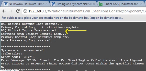
I got the following error at the time of deployment instance: error-307743:
We can see that something is going wrong with loop DI DAQ is started.
This error does not occur, and I deployed this file 10s and 10s times without problem.
My system has 2 cards:
-PCIe 6343
-PCI 6723
The first thing I did to remove the DI of the 6723, the system very well deployed once, then the error came back
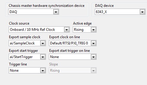
Finally, I watched the sync settings. They are defined as follows:
Their definition to None, working deployment. Then I put them back to DAQ, as on the fine above and all worked again.
Dig a little deeper in the present, I have noticed that if export sample clock is set to ao/sample clock error is back, despite the presence of strings in the AO list...
Been to you tips or file error system definition corrpution regarding these settings next to the info, that found the docs VS?
THX.
Laurent
You will have unexpected behavior if you are using hardware PCI and not connecting equipment with a cable RTSI.
The clock of the master device is designated with blue "BOLD", as shown on your screen. This device, as shown in the aid, which must be one that has at least 1 HAVE or AO. This device must then send the material sample clock to other analog devices (analog only!) in the system. This means that if you have other devices in your system that uses of HAVE or AO (and do not have the box 'disable the material unique point timed' checked)... they will expect to see an example of clock on PXI trigger 0 or RTSI 0.
If you use PXI... the sample clock is exported by the master on trigger PXI 0 and everything in the same backplane bus segment will see this automatically. If you use PCI... then you must either disable the hardware timing (not recommended) or acquire a RTSI-OR cable and follow this procedure that I just wrote to a colleague. (Ideally, we need to put this in the help in the future)
- Select the chassis page and designate (your multifunction data acquisition device) as the master of the chassis.
- In MAX, find your remote system, expand devices and interfaces
- Click with the right button on the chassis, then select identify-> external PC
- A right-click devices and interfaces and select Create new
- Choose cable RTSI-NOR and click on finish
- Right-click on the new cable RTSI-OR and add RTSI cable analog devices. These devices are necessary because they are the only devices with AI or AO is timed material (However some Councils don't support material as timing the 6704... which I do not recommend the use)
- Physically install a RTSI-OR cable between devices
-
Synch series AO DAQmx with DIO
There are not many examples DAQmx for AO series.
Can someone give me an example of how do I synchronize using outputs analog DAQmx on the digital master with exit/entry table on a Board of the slave?
I have an AO Series PCI-6723 (Dev1) and a DIO PCIe-6535 b the (Dev4) connected via a RTSI bus. I've defined the RTSI, using MAX cable and added the two devices.
Have had no success and cannot find a suitable example.
I'm on a Windows 7 computer that runs Labview 2012.
Thank you
Gretchen
I found a solution! It is complex, but it seems to work.
I used DAQmx export signals VI & DAQmx connect terminals VI.
See attached VI.
Gretchen
-
Operation Subvi don't update in the main program
Hi all
I'm having trouble with a VI I put together for laboratory research. I try to use two of the Subvi: one writes nine analog outputs through a PCI-6723, the other sends the commands M Code to a linear positioner through COM 4. Both work individually, but when I put in another VI, it seems that the outer loop only runs once. If I set a post and hit run, the track moves to this post but does not meet the additional entries. The tension control is doing absolutely nothing, predefined or not. The goal is that the two Subvi to run in real time. In other words, change the enum of the piece will automatically update the position and moving the sliders of tension with voltage indicators in real time and updated. I tried a few configurations without luck. Maybe it's because I'm trying to use a serial port and a data acquisition?
I have attached the main VI and Subvi for review. All advice is appreciated.
'Is it maybe because I'm trying to use a serial port and an acquisition of data?'
No, that would be a silly limitation of the language

There are a lot of problems with your application (on the other hand, you use a LabVIEW project to your hand and subVIs), like crazy in the Subvi DAQmx structures.
The real bug you see, that's the reason why you do not understand how a shift register stores the data: using shift registers initialized to the two subVIs, so overwrite you the values stored in each iteration. You should learn about Global Variables functional and motor action, so you can understand the problem. If you need work on your subVIs (also), you will need to change their behavior. In their recent form, they are not able to do what you want... Do not have a state machine for the subVIs, use actions: Init, check, change, close. Therefore, it is very important that your subVIs only perform one action at a time. Finally, when you stop your hand while loop in your main VI, you call the two subVIs with action command 'Close' to close and delete tasks properly.
Here's some reading more: http://forums.ni.com/t5/LabVIEW/Community-Nugget-4-08-2007-Action-Engines/td-p/503801
-
Tiara dac combined with the NI PCIe-6259 does not send the data
Hello
I have a card OR PCIe-6259 & DIAdem 11.2.0 (version 2010) on a windows 7 PC.Inputs outputs & analog analog + digital are configured in MAX 9.8.0f0. (Global virtual channels)
When I run a dac, entered analog works perfectly.
Outputs analog and digital does not work. Only one of the four analog outputs give the value that has been send.
In the past, I had the same problems with this version of DIAdem in combination with a third party USB card, but this has been resolved by the new firmware & software drivers.
Someone who has had similar problems?
Thank you.
After trying many things, I finally found the solution.
In the output ==> pilot ==> options pilot "weighting the digital bus" must be verified.
-
Buffer FIFO output DAC on PCI-4461 and USB-4431
I remember correctly, there is a FIFO buffer on the output DAC of a PCI-4461 to approximately 2048 samples. Am I remembering correctly? What is the output DAC FIFO on the USB-4431?
Hi jmoses,
The FIFO on the 4461 is actually 1023 * samples (found in the page on record).
The 4431 does not actually list a FIFO size in the page on record, but any device that handles output clocked by material will have some sort of FIFO to avoid running out of data to generate. By using the Output.OnBrdBufferSize property node returns 4095 * samples - it is logical that FIFO would need to be bigger, given the higher latency of USB transfers. Unless you use on-board regeneration, the FIFO size should not typically be a concern since it is designed to be large enough to accommodate a continuous generation to the full rate of the device specced.
Action request corrective number 149512 filed with respect to the issue of the missing documentation on our USB DSA devices - I apologize for any inconvenience.
* If you are interested, the reason that the FIFO is not an even number of samples is the software limits the size of buffer to one less than the actual hardware buffer. This is necessary for us to be able to detect the difference between an empty FIFO and a State full of PEP (we use a reading and a pointer to write to manage the transfer of data in and out of the FIFO - we can say that the buffer is empty when the two pointers are equal and complete when the write pointer is a sample behind the reading pointer).
Best regards
John
-
DAQ + DAC... OR PCI-6143 + PCI-6731 vs only PCI-6229?
Hi, I try to control a XYZ stage using a feedback program in LabVIEW and wonder about my computer card options for the acquisition of analog data (1) analog inputs and 2 digital outputs.
One suggestion I've gotten is the NI PCI-6143 of data acquisition of analog inputs, more the NI PCI-6731 for digital output to analog.
However, I wonder if the NI PCI-6229 can do the same thing that these 2 cards together can do and for a fraction of their price. The only question I can foresee is a slower rate with the PCI-6229. Other problems with this idea?
Please notify.
Thank you!
Hello clas004,
The PCI-6229 looks like it would be ideal for your situation. According to the two connectors are concerned, the 6229 has two front end connectors. If you check the 622 x specifications OR and look at the stitching down, you can see what is sent to each connector. Since you need 3 analog outputs, you'll need a cable and a block of endings for the second connector as two of the AO signals are on each connector. For cost-efficiency, if the noise is less of a factor for the signals of the AO, you might consider the block of CB-68LP-unshielded endings for the second connection.
As far as the compatibility of the PI functions are concerned, it is likely that they will work, but PI would be able to answer this question the best.
I hope this is useful,
-
Card PCI NI4461 CAD output anomaly
Hello
I use NI4461 PCI Card for a frequency response Analyzer application. Red I have a specific profile waveform to be generated using a DAC card. I tried to use the NI4461 card for this. But for DC output function calls, I get a glitch until the waveform gets stabilized DC output value. The same observation was repeated when the card has been tested through measurement and automation. Is this due to a limitation in the map? This card can be used for general applications of DCA?
Kind regards
Melanie
The "glitch" like this look? :
The 4461 is a material of acquiring dynamic signals with all anti-imageries features and anti-aliasing with this designation. The above acquired signal is the expected behavior because embedded filters attenuate the signal components with frequencies above 0.4 * Fs. If you see something different, post a screenshot and a code for the community can help more.
Generally, dynamic signal acquisition devices are designed to generate and acquiring dynamic signals such as those found in audio applications and vibrations. Use devices series M and X series to get the best performance for the applications of DC value.
Maybe you are looking for
-
Solve this linear system HP50g
Hi guys,.I am an engineer in electrical engineering and have to solve systems of linear equations on a regular basis, so that the functionality is very important for me. Everything works very well, 95% of the time but sometimes I meet systems that th
-
I need Skype on HTC Mozart is possible
-
Confusion between the Satellite A200-13O and A100-784
Hello... Please can you help me decide which laptop I will buy. The concern here is the difference in performance between the "GMA 950 up to 256' in the A200 and the" 128 "in up to the A100.". " Is there a significant difference in performance (all g
-
BlackBerry Q10 how to save my text messages on BB Q10 email?
I saved my messages before with my 9670 - what happened to 10 BB? We're going backward rather than forward?
-
Windows has stopped the device because it has reported problems. Code 43. Something with the generic bluetooth adapter. What should do? Original title: Please help