PXI-6284 entries
Nice day!
I have a question about PXI-6284 devices entries. This material spent ADC per each channel or channels work ith the multiplexer?
BES cordially, Vyacheslav.
An ADC on M-Series. Reference to the scanning speed to see if it fits your application.
The S Series DAQ devices have dedicated ADC per channel.
Tags: NI Hardware
Similar Questions
-
How to set up the PFI lines as input to PXI-6713 module
Hello
I have 6713 PXI module in my chassis PXI-1044. I have configured the PXI-6713 module to geneate some analog signals to my Board of Directors.
Council inturn process this analog signal and answers in return the status signals through a registry to the Board of Directors. In my application, the status bits in the register state of the governing body are mapped on the PFI 0:3 bits of the PXI-6713 (pins 11,10, 42 and 43) module.
My query is how can I configuration lines PFI as 6713 PXI module entries to read these status bits?
May be less than the explanation could give you little more information w.r.to my request.
When I use NI USB - 6008 module to read the same bits, because this unit has 12 e / s digital, I was able able to read the status bits in the last 4 digital lines by setting up those digital lines as input.
In the PXI-6713 module, I have only 8 digital lines. These 8 digital lines I used to send digital signals to the Board of Directors. I find myself with no digital i/o. Therefore, I could not use these digital lines. I'm left with only one option to use. Joana re PFI lines. Also the bits of status in the axis of the room are mapped such that the bits can be read through the PFI lines.
I was wondering do we have any example code to use inorder to read these status bits to the Board of Directors using the PFI lines.
Please let me know if you need more information to help out me.
Thank you.
Hello
When using the PFI PIN as input, you can individually configure each PFI for edge detection or level and the selection of the polarity. This information of PFI are referenced in the manual of Series DAQ Analog Output on page 6-1 (http://www.ni.com/pdf/manuals/370735e.pdf). Unfortunately, the PXI-6713 PFI lines are able to time a signal input and output for functions, AO or counters/timers. The ability to create static DI of the PFI lines is not available for the PXI-6713. However, some cards have this capability. The latest National Instruments products with PFI lines have the option of setting as PFI lines:
- Static digital input
- Static digital output
- Input signal of sync for functions HAVE, AO, DI, or counters/timers
- Output signal of the calendar functions HAVE, AO, DI, or counters/timers
(http://digital.ni.com/public.nsf/allkb/14F20D79C649F8CD86256FBE005C2BC4)
When the static value such as DIO, PFI lines are assigned to a different port (for example. PFI0-7 is Port1). More details on this subject can be referenced at:
http://digital.NI.com/public.nsf/allkb/DA2D3CD0B8E8EE2A8625752F007596E1
http://digital.NI.com/public.nsf/allkb/862567530005F09E8625677800577C27
-
It seems that the failures were the result of a connected PXI-6704, not the module cRIO himself.
The error is returned for the 4th time in about 2 years, but this time is not clear. We went to swap the PXI-6704 (entry at the cRIO module) Board with a known good and saw some pretty spectacular level damage. It is clear that a small area of the PXI Council was on fire at one point, and other areas of damage likely heat/current.
The damage seems to be centered around a blown diode, but we are not sure of the exact cause. It doesn't seem to be damage to the chassis PXI itself or the adjacent cards. We have to assume that the Council comes to the soul. It is amazing that the only indication there was a problem of this magnitude during the operations was one out very rarely bad power supply of the card.

I'll post again if this error of DC offset ever comes once the card has been replaced.
-
SE AcceesViolationException NationalInstruments.DAQmx.Task.UnregisterAsyncWaitHandle
Hello
I use my own .net application which communicates with NationalInstruments.DaqMx.dll (version 9.7) in order to activate NiDaq in the following configuration:
Chassis PXI-1033 at two locations PXI-6284, measure differential voltage. This app worked already for a few months and has been tested under high performance - high sampling rate and long hours, without no problems so far. Recently, we tried a new use case - short sessions (60 min) measures running in sample rate = 100 and samples per channel = 100 after a few iterations, we continue to get access violation exception:
Exception info: System.AccessViolationException
Battery:
to NationalInstruments.DAQmx.Task.UnregisterAsyncWaitHandle (System.Threading.WaitHandle)
at NationalInstruments.DAQmx.Internal.DaqAsyncResult.AsyncOpDone)
at NationalInstruments.DAQmx.Internal.AnalogMultiChannelMemoryOptimizedMultiSampleReadAsyncResult.WorkItem (System.Object)
at System.Threading.QueueUserWorkItemCallback.WaitCallback_Context (System.Object)
at System.Threading.ExecutionContext.RunInternal (System.Threading.ExecutionContext, System.Threading.ContextCallback, System.Object, Boolean)
at System.Threading.ExecutionContext.Run (System.Threading.ExecutionContext, System.Threading.ContextCallback, System.Object, Boolean)
at System.Threading.QueueUserWorkItemCallback.System.Threading.IThreadPoolWorkItem.ExecuteWorkItem)
at System.Threading.ThreadPoolWorkQueue.Dispatch)
at System.Threading._ThreadPoolWaitCallback.PerformWaitCallback)
Keeping the sampling rate 100, but his definition of samples per channel at 1000 seems to solve this problem.
Can someone explain to me what is the cause of this exception?
Thank you
Hadas
-
Constant time of entry for the PXI-6255
Hello
I connect a fairly high resistance at the entrance of a card PXI-6255, and I'm worried about constant time to entry are perhaps too big. I want to know is what is the ability to input of the card, or at the very least, what is the time constant for my setup? I currently use on 200kOhms, and he couldn't really do much lower. Thank you.
Hi kyh637
NEITHER x 625 specifications
http://digital.NI.com/manuals.nsf/WebSearch/210C73CBF91128B9862572FF0076BE85In the specifications is mentioned that the impedance between HAVE + and GND AI is > 100 GOhms parallel 100 PF.. Thus, the input capacitance must be 100 PF.
The reason why you might want to know that this is to determine the time, I guess. If so, there are graphic sedimentation on page 2 of this same document specifications.
See you soon!
-
Example one an entry of my analog PXI-7841R DAQ
I want to sample an analog input from my PXI-7841R AI0 to. The issue I'm having is when I drag the entry of my project in my VI, the element is defined as a signed integer value, and I can't change it to a floating/double. Why is this? I am experienced with LabVIEW; However, this is my first appointment LabVIEW FPGA development.
Help, please! Thank you!
I have it. Thank you.
If the manual gives me this forumla:
Gross = (voltage x 32768) / 10.0v
So if I wanted to compare the entry with a value of 1.5 volt analog, I could use the formula to get the gross value of 1.5V and compare it to the AI0 directly on the correct FPGA?
-
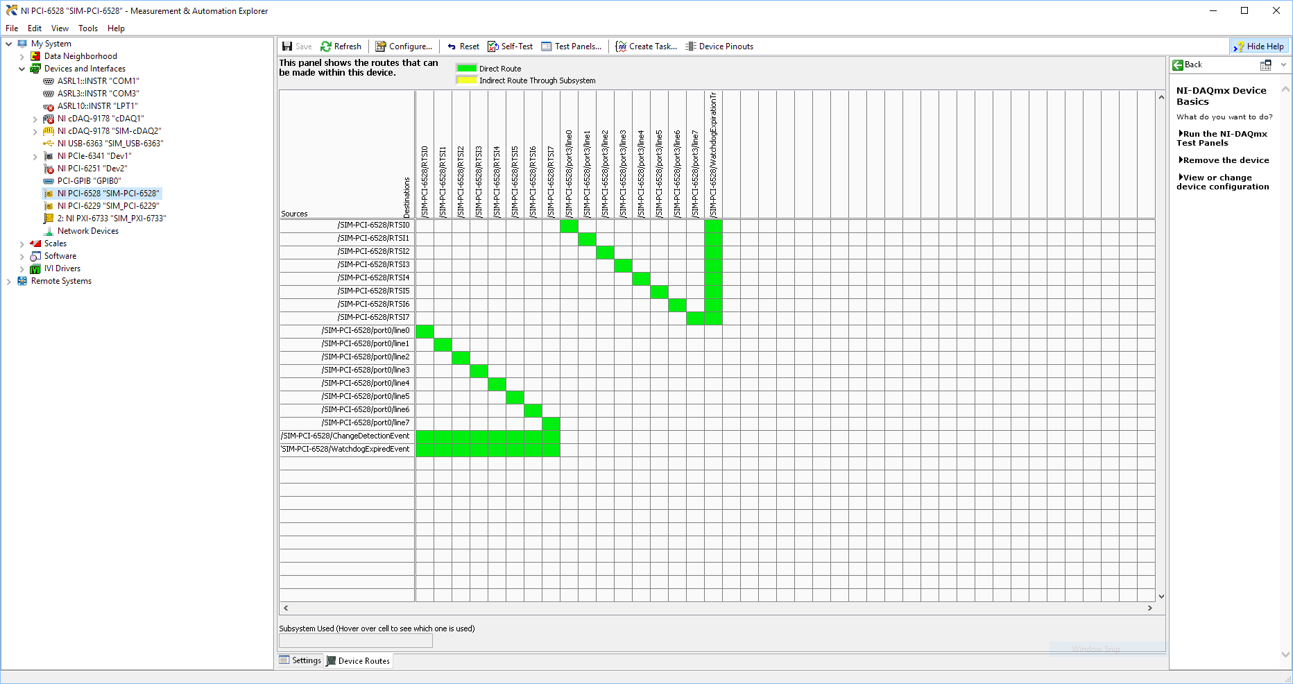
Using SMU 6612 to measure PXI-6528 pulsewidth channel - channel is not available.
Hi all
I use SMU 6612 card counter to measure the pulse width of the signals to PXI 6528 DIO card. These two cards are in the same chassis PXI (NI-SMU-1065). I could measure the pulse widths using the example LabVIEW 2013 Counter - pulse width of reading and (over) frequency example of .vi. However not all channels of the PXI-6528 map appear in the drop-down list of channels on the pulse width can be measured. Try to connect any other channel that those which are available in the drop-down list returns the error. On the PXI card port 6528 0,1 and 2 are entered ports and port 3-5 are output ports. I can measure the pulse on port 0, 3 width and line 0 port 1 and 4.
Can someone explain to me why don't see port 1 or port 2 channels in the drop-down list or force the VI to measure the width of pulse on these channels?
I can plug PXI-6528 external input channels SMU 6612 counter input channels and measure the pulse width, but if possible I'd like to avoid the external wiring between the 2 cards.
Probably not. Unless the routing plan is in fact reversed as it seems a bit sorta that. As stated on my system, you can route * of * a port of entry * to * RTSI, or you can route * of * RTSI * to * one output port. This does not make much sense to me, but that's what I see:
If the routing card * is * reversed, your only likely workaround without physical wire would be to generate impulses in question of port 3. It's pretty clear that 1,2,4,5-tetrachlorobenzene ports have no ability to interact with the bus timing, physical wiring would be the only option.
-Kevin P
-
Hello
I use a PXI-4070 DMM and DotNet "SoftwareTriggeredMultipointAcquisition" example
I want to trigger the DMM4070 with the AuxTrig entry to the front of the instrument.
This works very well, but how can I change the time out the of triigger?
It is now on 2000msec. I want to 10000msec.
When I us the example and do not trigger in the 2000msec I get error message saying:
ModularInstruments.NIDmm: The operation did not complete in time maximum allowed. Timeout: 2000mS.
Error code:-1074126845Thanks in advance
Wissam
Hello JaredRo
I can set the time-out period now.
Problem solved. Thank you Manny
With greetings
Wissam
-
While with PXI-5122 digitizer loop counter
Hello world
I am a beginner of products NOR. Currently I use the PXI-5122, 2014 Labview for the ultrasonic signals. I have a problem when you count the number of signals using an external trigger (by a function generator) source. When I trigger the digitizer under 50 Hz, the meter is working properly (a single trigger = a signal). With a frequency greater than 50 Hz of trigger, the meter is malfunctioning. For example, with the shutter to 50 Hz and 500 number of signals, the counter takes 10s to get data. But, with the trigger of 100 Hz and 500 number of signals, the acquisition time was always around 10 s.
You can see the code in the file attachment.Please let me know if you have any suggestions or recommendations for my situation, I would appriciate that.
Thanks in advance!
Best regards
YouWorldALoneMe,
Looking at your code, you're software re - trigger your device. With your Setup, you configure the digitizer to hold a single record acquisition in your "A - Scan.vi". This VI opens the resource OR-SCOPE, configure, captures, returns the data, then closes the resource OR-SCOPE. It then does this for each unique A-Scan that you do and would be the reason that b Scan.vi takes so long. It appears then that fewer than 50 Hz, this reset any software and reconfiguration and the acquisition can occur without missing a trigger, but more than that, your triggers occur faster it takes to do these things.
What you need to do set up the digitizer to a multi-record acquisition. This is done using the 'niSCope configure horizontal timing.vi' and wiring in a number higher than '1' in the entry "number of records". "You can find an example of how to perform a multi-record acquisition if you open the Finder of example OR > material input and output > Modular Instruments > NOR-SCOPE > Getting Started > niScope EX Multi Record.vi.
In this example, the digitizer is only once configured, and it returns all the documents requested at the same time. For your application, each record would be a simple Scan of A, and then if you configure 500 files, your B-Scan would be 500 wide. This time allows the material to rearm between triggers that is much faster to do it in software.
For a verification of more complex example out (in the finder of the example) "niScope EX Multi record go get more available Memory.vi"
Kind regards
Nathan P.
-
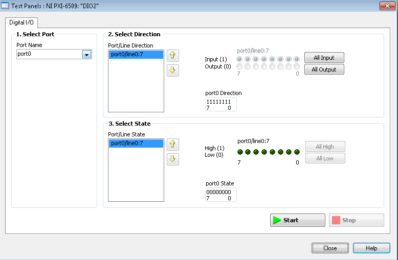
Individual access to the inputs and outputs on a single port (PXI-6509
Hello
I use PXI-6509 and this sentence taken from the Manual:
"You can use each of the DIO lines as the input to a digital static (DI) or digital output (DO) line"
leads me to believe that each individual DIO can be defined as input or output (even within ports), but picture:
shows that these ports can be defined as inputs and outputs in the same port.
On another card 6284 with DIO, I can put them individually.
Can someone confirm that the 6509 is correctly?
Best regards
Adrian
-
Please see page 4 of the specifications for the device. The signal that I'm trying to measure through a shunt 30A: 300mV, but in most cases, the maximum value is about 10 A/100mV. The readings that we receive are not clean and are quite loud, when the hope is that they are quite clean.
It seems that the smaller card voltage range is +/-1.25 V. According to the manual, the absolute uncertainty according to the table is 740 uV (or 0.74 mV). I watched it and it was quite high. I mean in 2A (20 mV) absolute uncertainty of 0.75mV is 3.75% and it is quite high. I realize that we use only about 4% of the voltage range and it is a problem, but I still think it could be better that it's - am I interpreting this right?
If I interpret it correctly, then is card on par with the industry standards?
Hello
Please clarify, I was more in the way of solving problems to try and get the best representation of your signal! Take a look at this article by NOR retailer the absolute accuracy. You can calculate this using the values in the table on page 4 of the manual you mentioned.
How to calculate absolute precision or the accuracy of the system?
http://digital.NI.com/public.nsf/allkb/8BA2242D4BCC41B286256D1D00815B90
There are three ways to calculate absolute precision in anticipation of your system design, although I'll add the specification on page 4 of the manual I believe is the number planned and tested by NOR. I apologize because I'm a little busy right now or I would run the numbers myself.
Absolute accuracy specification is a signal that properly uses the +-1.25V range. A 0.74mV absolute precision in the schema of a 2.5Vpp signal is less than two-tenths of a percent error (0.185%). There are modules (as you mentioned) for smaller ranges of entry, that's why you have seen a performance much better with the-range 0.5 to 0.5. You might consider to amplify the signal in the range of +-1.25 to get the best performance with the PXI-6123. Although the distortion seems to be important in your application, using only 4% of the available range is just a case do not use the material best suited to your application.
Kind regards
Train of Finch
-
Synchronize PXI-8512/2 and DAQ, PXI-6220 CAN
Hello
I read some examples and other posts on the topic "sync", but I need more information.
I'm using a PXI-8512/2 with an older application, based on the API of frame. Several frames are transmitted and received periodically, and I need to enter a unique ID of arbitration which has a cycle of ~ 5 ms.
At the same time, I need a task of data acquisition (analog input) with a sampling frequency of 1000 Hz.
The challenge is, I need to have the same time base for the analog input and CAN.
As far as I understand, the timestamps CAN are created in the PXI-8512. The timestamp of the start of the DAQ tasks is based on the time of OS (Windows).
Transmission/reception CAN must be running still (to perpetuate the ECU), and the data acquisition task will be triggered manually.
I found the example '\nican\Frame - base with NI - DAQmx.llb\CAN Frame entry API DAQmx Input.vi'. It fits my needs? There is a comment saying: "the departure of AI uses the same sampling as CAN. What it means? The sampling frequency of my CAN is fundamentally different from DAQ. But I have to be able to associate each sample DAQ for a CAN of armature (same time base).
Thank you for any information helping to clarify.
Concerning
Hello
Sorry, I don't know why I thought you had an X-Series. There is also an example for the other series with the XNET driver:
Synchronize PXI - CAN with analog DAQmx of entry (using the PXI-Clk10) .vi
Kind regards
Heinz
-
PXI-5402 IVI TestStand 4.2 returned "niFgen_InitWithOptions" resource not found
Hi, I am very new in TestStand.
I hope someone could help me.
I have a complete sequence in which an ivi should initiate a PXI-5402.
(It is an old sequence that I inherited. It is now my job to make it work again).
We have another system with a PXI-5401 (appears to the MAX as traditional-DAQ) which works very well with this sequence.
I created a new sequence in order to simplify troubleshooting with just "IVI Fgen" step.
When in click on 'Validate' and uncheck "Simulate" and hit "Init", I get:
niFgen_InitWithOptions returned an error:-1073807343 (0xbfff0011). Insufficient location information or the requested device or resource is not present in the system. If the resource descriptor is a name of IVI, it must match the entry in the store of IVI Configuration in a case-sensitive manner.
Source: TSIviStepTypes [error Code:-31619]In NOR-Spy I get following error
> Status: 0xBFFF0011 (VI_ERROR_RSRC_NFOUND)I think that I have configured all correct. Please see attached screenshot.
I tried different names IVI-logic...
For this remove as first cause, I direct the pilot Session that appears correctly on the iviConfiguration of reference.Thanks in advance
OK, I got it...
This is the well known problem with DAQmx Configuration in MAX.
Described in the title:
http://digital.NI.com/public.nsf/allkb/22CF7E6B27B6995B86256DDB0058F39B
I had post a logic-name link with DAQmx device instead of PXI-Device.
Thanks anyway.
-
Use the PXI-2630 terminal block in a matrix configuration?
My apologies in advance for the length of this post!

I use the PXI system with PXI-2530 switch modules, related to a series of USE with PXI-2632 (1W matrix 8 X 16) connector blocks and a PXI-4071 DMM for each switch module. My request, uses the PXI system for measurement of current and voltage external to verify and/or benefit from restraints of reliability. A requirement of the application, therefore, is that there must be a ride from DC through each USE with change of the minimum impedance as the application between its "bypass" mode switches and its mode 'measure '.
I used this Setup with connector blocks of matrix in conjunction with one of our test systems, and I am satisfied with the results. I started working with the Test System, has no easy connection to catch HAD, I needed to build a kind of interface the PXI system and a resistive faced load HAD, it was not difficult to build in the wires that attach to the Terminal screw of the 2632. He did turn into a nest of a coded son rat I did my best to keep clean and tidy in different bundles, however. Fortunately for the cable fasteners!
My next task is to use this application with system B Test, which has an interface of pines buck header with which each signal that goes to or from the DUT can be obtained. No welding or pass the wires through the openings where the designers have no intention of son to be stuffed. I intend to build a break-out Board that allows simple connections between the modules PXI and the number of Test B system which we have or will have in our laboratory. In order to simplify the configuration/installation, I want to reduce the number of connections to terminal block screw. Preferably, I would like to completely remove the screw terminals and use lever-based connections where I can't have mating of the headers. The PXI-2632 terminal blocks unfortunately use Terminal screw.
In matrix mode 8 X 16, the closing of the PXI-2530 switch kcom1, 3, 5, 7, no matter what points in the array are connected. A link between the row of right and column C is done by closing the switch corresponding to k (16R-C). I checked using the Soft Front Panel.
I also have a number of connector PXI-2630 blocks. These are intended to be used with the switch module in one of its MUX modes and include 8 banks of connections of the header 2 X 9 pins. In the the 2530 documentation and 2630, I identified that switch k-x is associated to chX output pin, ch0-15 related to the pins 1-16 from Bank 0, C16 - 31-associated pins 1-16 of Bank 1, etc.. X = 16 B + P-1. PIN 18 of each bank is used for independent MUX topology comX. Pines multiplexes sixteen seem to correspond to the sixteen columns of the matrix, with eight common lines corresponding to eight lines.
Here's what I would do, but I would like to ping the forum to see if anyone tried something similar and wisdon to share the thought:
- Make custom cables which connect the pins 1-16 of all eight banks 2630's header with a single Ribbon connections 16 son carrying the signals emitted by the interconnected banks (poles!).
- The custom cable bundle will also include a wire connected to the pin18 of each of the eight banks (line connections!)
- 24 total wires in the harness will end in the header connections who will probably partner by the lines that I currently connect to each object to be measured.
- Make additional harnesses that interface with the Test System B header pins.
- Make a map of derivation using band Council or a similar material to provide header pins to connect the two above custom cables and allow the connection of other elements such as resistors using Terminal level.
I checked this concept using the Assembly of 176 pins four terminals, like a bunch of little pieces of wire and cable. Are there other issues that I have to configure, such as the elements of a terminal that establish physical components of the switching topologies? The bowels of the PXI-2632 provide more features than the interconnection of the sets of eight sixteen pins? The bowels of the PXI-2630 connect elements that do not allow my proposed scheme?
I appreciate the suggestions and all entries!
Thank you
Jeff Zola
Hi Jeff,
First a correction to my previous post: 2632 Terminal has no reed relay protection resistors as I said earlier. The resistance that you were referring to the 2632 and those that I confused, is there to connect the columns of the switch. Resistances have a resistance value zero and act as the electrical connections. The 2632 connects columns c0 to c16, c17 c1, c2 to c18 and so on. Switch cards 2531 and 2532 have the protection relay reed on board resistors.
As for resistance in the map that protect the reed relays, they are generally very low and do not significatly affect even small tensions that pass through the switch. The resistance won't affect all currents in the map. Any effect that the resistors have on tensions will be with the precision of the switch card specifications.
Thus, to address the other issue in your post, there is no resistance in the connectors because they are not necessary.
-
PXI-5421 Signal routing to PFI4 and PFI5
Hello
I am trying to route bits 0 and 1 of a waveform I generated using a PXI-5421 AWG group work PFI5 and PFI4 respectively for the ports. What seems to happen, this is the first installation is written the second set so that only one PFI port is set up. I've attached a screenshot of a section of the configuration of the VI. Can two bits of a waveform being routed to two ports separated the IFP at the same time?
Thank you
Steve
Hi Steve,.
Yes. There is data on the PXI-5421 4 markers, and each can be configured with unique values for each of the attributes of data marker. To set up the markers of data independently, you must specify a 'Active Channel' for the polarity of marker data and number of bits attributes. So in your example, you would just need to add an entry "Active Channel" on your property node above the attributes of marker of both data and wiring in the "datamarker0" to set up the first brand of data and the "datamarker1" for the second. "NiFgen waveform Arb marker" shows how to do this. Do not wire the active channel range cause really all markers 4 data to configure when the value of each attribute of data marker.
Hope that helps.
Maybe you are looking for
-
HP 250 G4: System Properties showing the wrong GHz speed
Hey everyone, I recently bought an HP i5 6200U Tower, according to intel, it suppose to be maximum of 2.80 Ghz, but on my task manager and system properties, it displays 2,40 Ghz, at the same time sometimes to the task manager the speed goes all the
-
How to connect my printer, my lap top and my WiFi network
always asked me the code for the printer I have try but always disabled so I printed the serial paper any thing evry number, but I can't find the code so can you answer me soon please. Thank you
-
135W adapter plugin... Stop the W510... Always be powered by USB
Just found last night... my laptop cooler with USB still work after I closed the laptop. But it's not going to work if I plug the charger 135w. Is this normal or not? I tried on my T61. No question too...
-
How can I keep another installation of users contained in their login?
Greetings! I share my PC with my wife (who has his own PC but who choose to use mine more so I'm going to h-e-double hockey sticks faster). Well, it downloads and installs Games http://www.gamehouse.com and download games for PC | Game PC secure & sa
-
What the series different Cisco MSE 3300 wireless (WLA) Cisco location appliance?