SPI, C#, C++, PC
Hello
I wondered if there is a way to use the SPI (Serial Peripheral Interface) of the computer in c# or C++. Next to it is the bus system the use of sd and mmc cards. There is a way to do it on .net Micro Edition, but I have not found anything on the PC. The driver of the SPI interface is calles sdbus.sys can there is a way to use it?
Thanking you
Soitis
http://social.msdn.Microsoft.com/forums/en-us/vcgeneral/threads
Try to post in the Forum above.
It comes to the Installation of Vista instance.
See you soon.
Mick Murphy - Microsoft partner
Tags: Windows
Similar Questions
-
What are the twins in the bar address, friend being spyed on?
Sometimes, but not always, a small pair of binoculars will appear at the beginning of the address at the top of the display bar. This means that someone spying on me? I ran virus scan but nothing shows up!
You can attach a screenshot?
- http://en.Wikipedia.org/wiki/screenshot
- https://support.Mozilla.org/KB/how-do-i-create-screenshot-my-problem
Use a type of compressed as PNG or JPG image to save the screenshot.
Do you mean the purple icon that you see when you're in private browsing mode?
Make sure that you run not Firefox in private browsing mode (permanent) (don't forget the story never).
- Tools > Options > privacy > Firefox will be: "use the custom settings for history".
- Uncheck the box: [] "always use the navigation mode private.
-
where and how to get the new Firefox add - one of who is spying on us. Please mail to...
Heard speak adds the new on Fire Fox. Where and how to get the new Firefox add - one of who is spying on us. Please mail to maheshubhayakar at rediffmail.com
edited by email address - moderator
It is helpful if you provide a link to the article you were reading.
-
Some strange things have developed to the end that suddenly somewhat concerned me that someone keeps track any activity on my macbook air.
I see nothing wrong in the file of applications, but I have to admit that I am somewhat a sucker when it comes to such things.
I checked the Applications system/preferences/Remote Login. It shows that it is on the off"" position.
I checked the Applications/Utilities/Terminal. It shows the following:
"Last login: Tuesday, 6 Oct 15:06:48 on console.
"Steves-MacBook-Air-2: ~ stephent * $".
There are, installed on my computer, an application called "Remote Desktop connection" which has the Windows flag as its icon, but it seems unusable because a ' windows computer is not found. "
What recommendations do you have for me to check that my keystrokes, e-mails, files generated, etc. are not followed in any event via remote access? Community, I thank you for your comments.
MacBook Air OS x 10.
The application "Remote Desktop connection" is a legitimate application which allows connect YOU to a remote PC. An older version of this app comes with all older versions of Microsoft Office. Therefore, unless you have other symptoms that someone spying on you, they probably aren't. Have the "Remote Desktop connection" application on your Mac is not an indication of espionage then you can be more comfortable.
Is something you should check out: 'System Preferences' > 'Security and privacy' > 'Firewall' > and make sure that your firewall is "ON".
-
LabVIEW FPGA SPI accident - SPI OR IP address for example - R series OR
Hello
I am trying to run the series R - sample project NI SPI FPGA Simulation.lvproj that comes with the SPI IP OR on a real FlexRIO FPGA SMU-7976R target with an attached digital adaptation NI 6581 B Module. The example is for a PCIe-7841R but I wore during my target FPGA, follow these steps and made additional changes to try to make it work with my set-up. I learned that FlexRIO FAMs CLIPs do not work with nodes in office had so I know I can't simulate the project originally planned so I will try to use FPGA to e/s node host side (open FPGA vi reference) to implement the actual hardware.
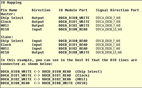
My first question concerns my configuration of the adapter module e/s and selection. I added the IO Module (NI 6581 B: NI 6581 B channel) for my project and selected the channels as shown in the table below. I have a real physical hardware connection as described below using two NI SHC68-C68-D4 cables and a break-out Board.
I changed the names as well:
I selected these DIO channels because I wanted the DDCA connector to be the master and the DDCB connector to be the slave. In addition, in this CLIP every eight channels of i/o has a write enable signal. I have not used the Port configuration because I needed 4 available DIO channels and I saw DIO0-3. Is my logic of selection of channel vs correct Port here?
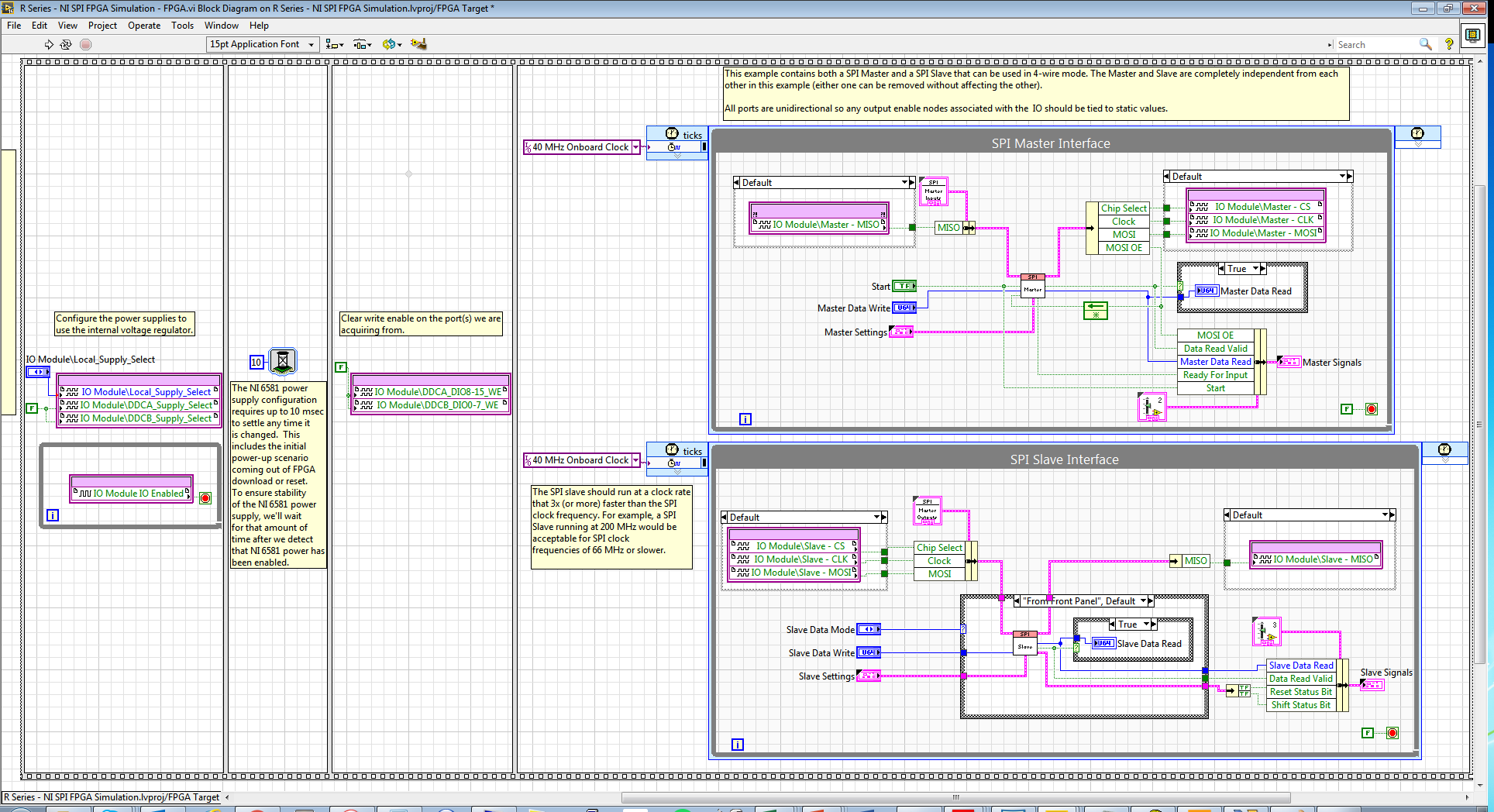
Following the same strategy that examples FlexRIO/NI6581B, I changed the FPGA.vi to include initialization outside of timed loops:
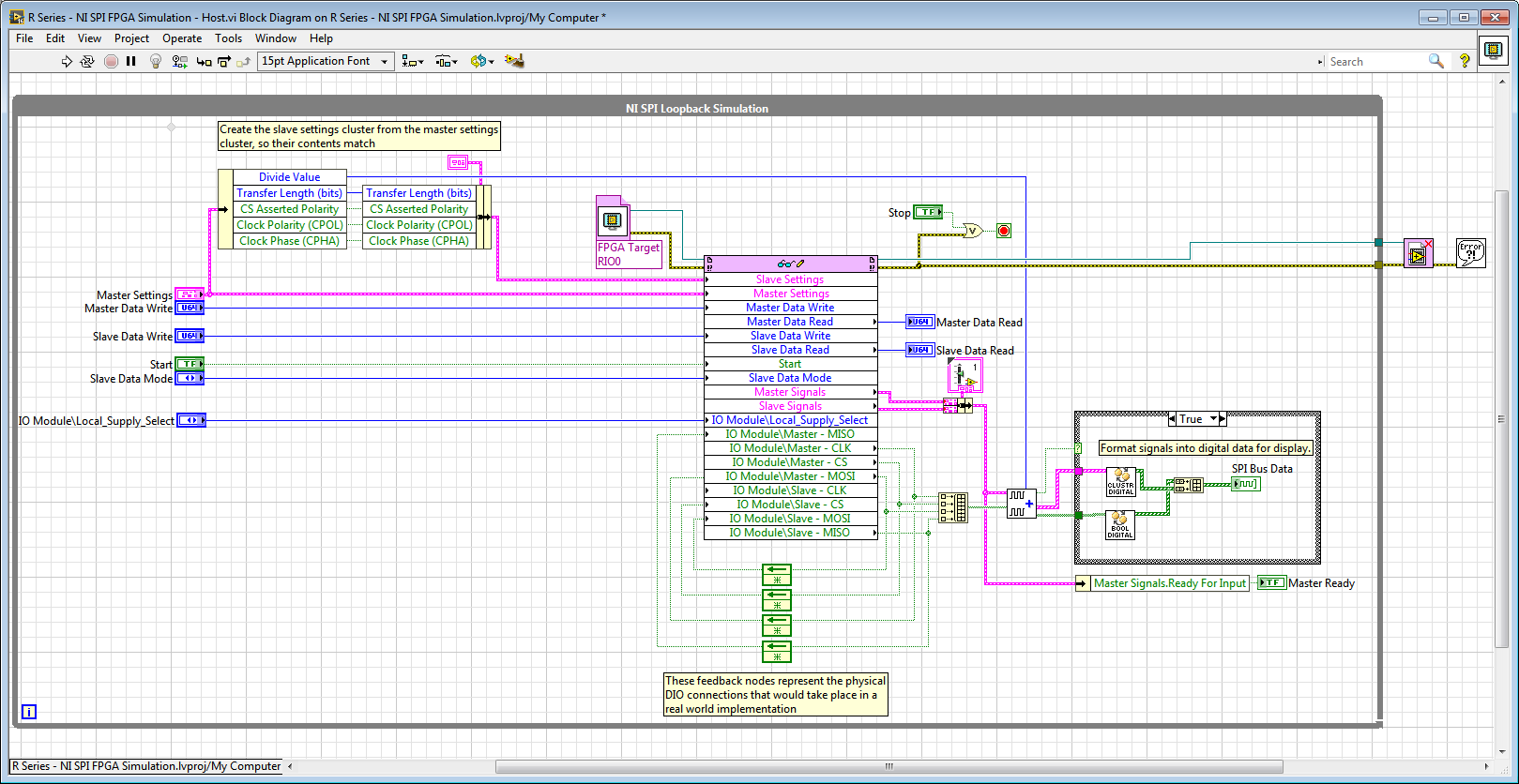
And in the Host.vi I have a node reference FPGA and wired loops of feedback accordingly:
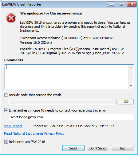
When I compile the FPGA and try to run Host.vi LabVIEW inevitably crashes with Crash Reporter below and must restart:
Does anyone know what I'm doing wrong here? My guess is that it has something to do with the CLIP/IOModule. Any help is appreciated.
Thank you
Scott
Hi Scott,.
I suspect that the problem might be related to the fact that your node open FPGA VI reference is in the while loop and trying to open a new FPGA reference at each iteration.
If you move outside of the while loop, it does not solve the crash?On channel vs port question, your logic seems reasonable to me, but I recommend to try it since this feature could depend on device.
-
Why SPI participates with clock select on 5761/2 scanners?
The CLIP reference for the 5761 5762 sample clock commit signal States, and "when going from FALSE to TRUE, updates the sample clock according to the settings defined by the signal of selection sample clock." Shipping examples bookends the rising edge of clock sample commit with SPI Idle check. Why the SPI is involved with setting the sample clock?
Thank you
Steve K
I have a requirement to PLL to IOModSyncClock, so if SPI become inactive within the time limit, should I give up? In other words, if SPI will not idle 10 ms after the rising edge of clock sample commit, so I am not locked (for example clock select = IOModSyncClock lock).
I would not abort, rather I'd throw a significant error that allows to recover gracefully or stop the execution. Otherwise, it seems that you have the correct impression on which should involve the remaining false SPI Idle. However, I think 10ms sounds a bit too short. I'd go with at least 100ms, probably closer to 1 s just to be sure. If it takes more than 1 s, then you can assume that something has not been configured correctly before you start setting the clock.
-
NEITHER USB-8452 - reach the maximum write SPI speed
Hello
I have a USB-8452 with the latest version of the software installed (2.1.2). The host computer is a Core i7. I am trying to achieve the maximum SPI write speed with the camera possible. I tried the basic block read/write SPI, SPI Scripting blocks and SPINNAKER streaming, but the first two have large delays between CS falling and the data being written (with so that delays in loop), and the last seems to be useful only for read operations.
Can someone tell me if there is a way of a) reduce the time of installation for basic SPI / SPI Scripting or b) writing different values in a single stream of SPI? Thanks in advance for any help on this issue, even if it's just confirmation that yes they is hard limits that cannot be overcome with the LabVIEW 8452 interface at this time.
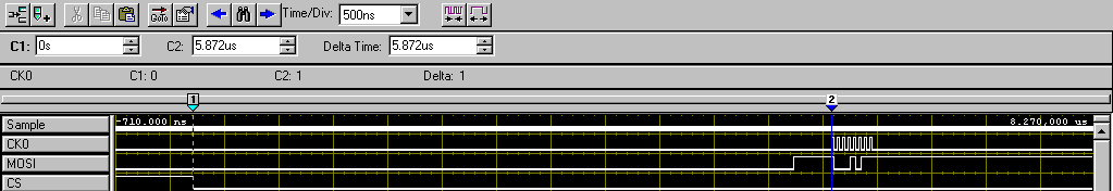
Here's the best I can do right now, as shown in my logic analyzer. Change of the SPI clock speed does not affect installation time and delays that are primary and secondary bottlenecks:
SPI read/write database-
Program: Basic Configuration followed by read/write of SPI block itself in a while loop
Main bottleneck: ~ 450 delay us into iterations of the loop (see Figure 2)
Secondary bottleneck: ~ 6 us delay between falling edge of CS and the first synchronization signal (see Figure 1)
Capture 1 - delay highlighting between CS falling and first SCLK pulse
2 delay highlighting between all iterations of the loop of capture
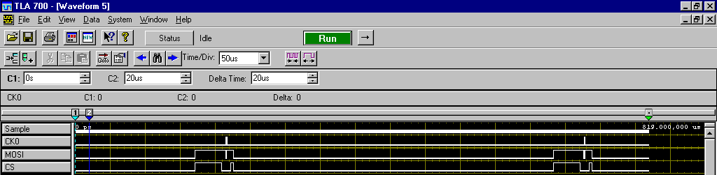
Scripts of SPI-
Program: Followed two Script blocks Basic Configuration run in a while loop (to check the two block to block and delay loop iteration)Main bottleneck: ~ 450 delay us into iterations of the loop (see Figure 3, space between the second and third images captured)
Secondary bottleneck: ~ 250 us delay between blocks of Script run consecutive (see Figure 3, space between the first and second captured images)
Capture 3 - highlighting delays consecutive run the Script and delays between while the loop iteration
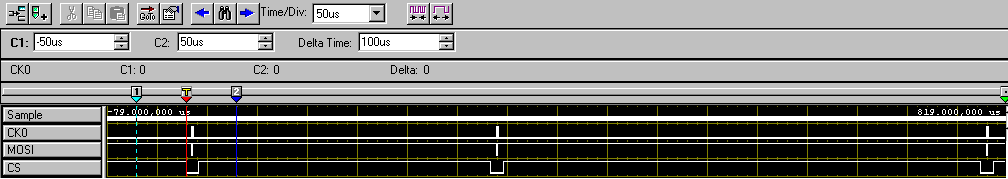
SPI in Streaming- It's the closest to achieve a fast writing speed, but unfortunately, it seems to be only useful for read operations (e.g., ADC), do not write.
Program: Configuration of the base stream followed by start of the flow block
Main bottleneck: impossible to write something else than the data value unique property "wave 1-> MOSI data." I can write a byte array to this property, but it will simply put all these bytes in an image and repeat this framework (see Figure 4) rather than go through each value.
4 - two bytes sent repeatedly using SPI capture stream. Delay of CS is finally good, but no possibility to change the MOSI image to image data.
Hi JBender1,
This show looks like what we would expect for a 8452.
If you need higher performance, I encourage you to watch using a card R or FlexRIO FPGA series for your implementation.
-
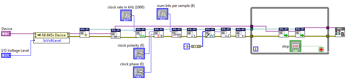
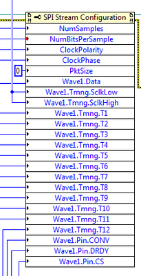
USB8452 - how to set a clock of 20 MHz SPI Stream mode?
Hi all
I can't really manage set a clock of 20 MHz SPI Stream mode.To set how often I use this property node (see image)
[for example to set a 1 MHz clock, I put:]- Wave1.TMNG.SclkLow = 50 (500ns)
- Wave1.TMNG.SclkHigh = 50 (500ns)]
And everything works fine.
When I try to put a clock of 20 MHz instead, I put:
- Wave1.TMNG.SclkLow = 2.5 (25ns)
- Wave1.TMNG.SclkHigh = 2.5 (25ns)
But, unfortunately, I receive a 25 MHz clock.
I know the USB 8452 can generate a 20 MHz signal, so I think I'm doing something wrong, but honestly, I don't know what to do.
I see that the entry for Wave1.Tmng.SclkLow/High is a U32, then perhaps it truncates my 2.5 to 2 (i.e. a 25 MHz clock), but given that the USB8452 can generate a 20 MHz signal I honestly don't see the point of this.Thanks for the advice/help,
FedericoHi Federico,.
as you can see in the image below, the number that you set is the number of clock cycle of BASIC that make SPI clock.
Base clock is 100 MHz, then the single 10ns resolution. You have to choose between 20 and 30ns or try to have 20ns high clock and 30ns low clock.
Teo.
-
Read only the SPI using the box USB-8451
I am using the NI USB-8451 box to read the SPI of a Honeywell digital pressure transducer data. The difficulty comes from that part of Honeywell uses only the SPI in half-duplex mode, meaning that it only transmits data, but does not require anything beyond the appropriate chip select signal and SCLK to start transmitting its 32-bit sensor data. To facilitate experimentation with the sensor, I bought a USB-8451 SPI Interface thinking I could easily configure the 8451 to read data from the sensor.
However, if I understand the situation, there is a problem. The 8451 considers full duplex data, i.e. a data word must first be sent to the SPI device in question before the unit will start to transmit back data of its own. And since the MOSI data writing periods, since this particular device starts transmitting immediately once a clock is applied, synchronizing the unused address data will cause the unit will return its data before the 8451 begins listening for data in return. The call used by the 8451 to write read action can be divided into the individual reading and actions of writing of any kind that I could discover.
Can someone tell me if I missed something in this operation or if there is some quick tips, that I could use to be able to use the 8451 therefor? Thank you!
Doug G.
Exactly correct. It's nice when things are easier than expected. Hope it works as easy as it sounds.
-
mcb2300 (lpc2378) SPI and external ADC
Hello
I use LabVIEW 2011 Embedded for ARM in collaboration with MCB2300 Development Council and MCP3204 12 - bit ADC chip. I try to use the base screws of SPI to communicate with the MCP3204. I enclose below the screenshot of my VI. Can someone tell me if this is a way of thinking? I would like to read the data from all 3 channels of ADC - 3 axes of the ADXL sensor connected. In addition, I have attached a few pages of the MCP3204 datasheet.
Thanks in advance
Hello
There is solution on NI Developer zone, which can help you - https://decibel.ni.com/content/docs/DOC-15231
-
Hi guys:
Sorry to post this question, but I really can't get it to work!
I can configure each SPI device and they work only, when I try to config 2 devices, I can't just two lines of CS to go up!
Note: Here is my code, I choose slave select 4 so it is easily accessible via SPI connector to the Board of Directors (PIN 14)... SS1 is pin 9!
Thanks in advance
I like your "main.vi" instrument, but unfortunately, I think the AD7476A driver was not designed with several converters a/d in mind, let's dig a little deeper.
"Declaring Slave Select" command limits the value 1-7, because the SPI device can drive directly only this amount of devices, each of them being validated in accordance with the SPI_FLAG registry. Notice that in the DMA transfer mode (case of pilot AD7476A) CPHA = 0 and SS pins are automatically selected at the beginning of each transfer: for each bit set to one in SPI_FLAG a low pulse will be generated to the corresponding pin! (These bits are set on a per activate slave select or declare slave).
He had been great if playback turn slaves, but isn't.
I'm in the island you will not wait 1 MSP for all a/d converters. The AD7476A conversion time is determined by the clock series: the pilot sets the SPI clock on the sampling frequency of 16 times. This is why must be given a higher value in the sample spent at BF AD7476A Control.vi clock:
For a system with converters a/5 n and 100 KSPS value must be 500000. Inter-channel delay is in this case 2 microseconds, so the difference in time between the first sample of the first string and 5th Channel is 8 us (almost equal to the sampling period), this could be a problem in some applications.However, more information is available in the description of the material (ADSP-BF537 Blackfin processor Hardware Reference ), documentation of device driver (C:\Program Analog Devices Devices\VisualDSP 5.0\Blackfin\docs), and drivers of source code (C:\Program Analog Devices Devices\VisualDSP 5.0\Blackfin\lib\src\drivers). Here, I would just say it seems circular buffer are not taken (see VisualDSP 5.0\Blackfin\docs \spi\adi_spi_int.pdf and adi_spi_dma.pdf) and move to solutions:
1 reconfigure the SPI to use interrupts and use reminders to go through program slaves using BF SPI Control.vi "Select/deselect"slave"(of course, each of the ointments pins must"Declare Slave Select"with BF AD7476A Control.vi or"Activate Slave Select"using BF SPI Control.vi). This will add overhead and, depending on the sampling frequency, you may lose a few samples. Also, there is a limit of only 7 slaves.
2. turn on DMA for a single word and switch slaves in the callback after each conversion result (of course, this will have the same disadvantages as #1).
3. Add a simple external hardware to automatically select the a/d converters (for example a counter + decoder clocked by one of the seven pins SS and reset using EIO). Then play with stamps to identify channels (example buffers 1 d with 5 items for converters a/5 n). This will add less overhead, reminders will trigger once a sample of all channels was acquired (or even better after n samples, if the length of the buffer is nx5, etc..)
All of these solutions, to open and close AD7476a driver only once in the 'main.vi.
#1 and #2 similar to your posted solution above but the command must be select/deselect for interruptions and toggle for DMA. The slaves should be put in exactly at the end/beginning of each word received.
-
Generation of SPI by using the b PCIe-6535
Hello
I have a data ready signal generated every 100uS or so by a SPINNAKER of slaves.
The SPI master must generate then 96 SPI clocks anhd captures data returned.
The process is repeated every 100uS. The SPI 96 clocks must be completed before the next event, hence the need for an ardware or RT system.
Would it not possible to program the PCIe-6535 b to act as the master of SPI that is to generate the clocks, store data, such as a Windows LabView program can probably pick up data without loss?
Or I'm looking for something more like a RIO?
References & code examples would be great!
-
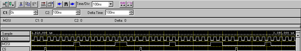
lm3s8962 - SPI and microSD memory
Hello again,
First I use LabView 2009 and its ARM corrosponding module.
I'm trying to contact the SD card on the set of the Star (yes I put an in) using the ARM SPI functions.
You need not use the SPI screws to access files.
Welcome to the universe "excerpts":Create a new project, drag the extract and... voila:
-
SPI Communication with PIC24HJ256GP210
Hello
I need make the SPI Communication with hardware PIC24HJ256GP210 in LabVIEW 2010 with NI USB 8451.I want to send 8 bytes data and receive data of 8 bytes of PIC. I'll send data byte-by-byte change the signal of the chip Select (CS). Before you send the data I will send ENQ (mark 3A) to check the status PIC, then after receiving ACK (Acknowledge as A1), I will send the data packet.
My test procedure indicated below,
- Setting clock polarity at zero (LOW idle), a second Edge clock Phase) and the clock frequency of 1 MHz to device NI USB-8451
- 3 sending data (ENQ) and followed meaningless data byte by byte, also change state Chip Select
- No explicit deadline has provided since the sending of the API takes 20msec to run
- Receive the acknowledgment of receipt (A1) of the sensor
- Send DataPacket [Eg: A5, 03, 02, 00, 00, A6, 2 c, DD] byte by byte, also changing chip select signal
- No explicit delay gave between each byte from API takes 20msec to perform sending
- Send 8 bytes , which means less data byte-by-byte, and receive byte-by-byte data PEAK
- Received all of the data of 8 bytes with an incorrect value
If please review my test procedure and give your comments if you have worked with SPI or if you have any input for my query.
Thanks in advance.
Note: Tie my code with this mail for your reference.
Kind regards
Nicolas.
Hello O_Proulx,
Thanks for your reply.
Communication SPI after sending the data we send again meaningless bytes, which equals how many bytes we would like to receive the answer System.So we cannot read the data in the same VI as you mentioned in the code.
My problem has been resolved. Byte meaningless, I need to send the file HEX .beacuse 'AB' has been developed in this way.
Kind regards
Nicolas.
-
Narrow ARM of SPI VI reference works do not for me LabVIEW 2009.
I use LabVIEW 2009 Embedded for ARM in collaboration with the Council of development of LM3S8962 and the MCP3008 10 - bit ADC chip. I'm trying to use the base screws of SPI to communicate with the MCP3008 - see the attached excerpt from VI to my current attempt. I can initialize the SPI reference, read two bytes of data from the ADC, but when I try to close the reference, the application crashes. If I am the narrow ARM of SPI reference VI in a diagram to disable, the program terminates normally, and I get to see my two bytes of data printed on the OLED. Any ideas?
Thanks in advance,
Stuart
Thank you!
Who takes care of the immediate problem. I really appreciated the quick response!
Stuart
-
Writing to SPI peripheral using the NI PCIe-6363
I'm writing a labview program to write to a simple SPI device using the DAQmx 6363. I found a library and examples of code and started using the "SPI - internal Clock.vi DAQmx".
http://www.NI.com/example/31200/en/
I believe that this is the right place to start, but I keep coming across mistakes that I can't locate.
200452 error occurred to the property Node DAQmx export Signal (arg 1) in Init IntClk Device.vi-> DAQmx SPI - internal Clock.vi
Possible reasons:
The specified property is not supported by the device or is not applicable to the task.
Property: DataActiveEvent.OutputTerm
Task name: _unnamedTask<18>
I found the vi the cause of the problem, but I'm not sure what the problem is yet. Any help is appreciated.
I believe that this knowledge base article contains the answer to your question. Follow the steps in knowledge base article to determine if the property node that you are using is supported by your card.

Maybe you are looking for
-
"use the custom settings for history" changes to "remember history" at the exit.
Whenever I change the setting of the story and the output, I come back to find that it has reset to "remember history".
-
Unlocking the phone (without access code or contact id)
iPhone 6 / ios 9.2.1 (13D15)CAN SIMPLY IGNORE THIS STEP (ACCESS CODE) LOCK the SCREEN AND KEEP HOME BUTTOM FOR TALKING WITH SIRI PRESS / ASK at WHAT TIME NOW / PRESS the CLOCK / TIMER / SELECT TONES /ACHETEZ MORES TONES / AND BACK... then the PHONE W
-
My iMac runs very slowly these days. Can someone help me with the Sub results of the EtreCheck know why this could be? EtreCheck version: 2.7.8 (238) Report generated 2016-01-28 13:17:35 Download EtreCheck from http://etrecheck.com Duration 09:04 Per
-
I can't transfer my photos from my phone to my computer. I can visualize very well on my phone, but as soon as I move into my computer the images are not all valid and I can't see more. I've only tried with pictures that I took with the camera on my
-
When will the CLIQ update the Android market?
I have an old market (grey and black). It is very annoying! I asked T - Mobile Motorola will update the market, and they referred me to the Motorola forums. Response from Detroit.