Transfer 1 d table using DMA FIFO of FPGA
I'm transferring a table 1 d of two U32, with a configured U32 FIFO for the host.
but I get the error because of the connection to different types of terminals,
It seems very simple, I found a lot of samples with a very similar treatment here, but I don't see the problem?
There is a loop of indexation of array... The write operation is therefore the element by element.
The operation of reading (on the host) can read several items at once (--> a table).
Tags: NI Software
Similar Questions
-
How is managed using DMA FIFO (target host) host matrix
Hi people,
I'm trying to pass an array of values of the host to the FPGA using DMA FIFO. Let's say 20000 items in the table. My FIFO host side can contain only 16000 items or almost. The data will be written element by element regardless of the size of the table or do I need to partition the table in small paintings before writing the FIFO method? Let's say that I write for the FIFO with berries small, 1000-element. The FIFO will read 1 element both of the side FPGA so the stream is blocked until I have at least 1000 free items on the FIFO method write, how he writes every 1000 the next setpoint at the same time? Or target values will be written permanently as soon as the individual elements are erased by the number of available items to write?
Hi Nathan,
Sorry for the late update, but I just thought that I should follow. I followed your advice and try it tested just for me (I probably should I have done it before posting). Turns out that the data table will write even if there is not enough empty elements to contain the table in its entirety. However, it always crashes until enough information is read and erased from memory on the side FPGA for the whole table. So if it's data that are constantly being played, it's always better transmitting data through in the form of smaller tables if you do not want to increase the amount of memory FIFO host OCCUPIES on your system. However, if you can afford the memory while you mentioned, you can always increase the depth of the FIFO on the host side. As I understand it, try to write more big berries to a host to target FIFO buffer does not diminish overhead costs (as is the case with a target to host FIFO) as it still passes an element at a time to the FIFO of FPGA-side without worrying.
Thanks again for your help.
Kind regards
John has
-
DMA FIFO of FPGA to host RT is full
I transfer data via DMA FIFO of FPGA to host RT.
DMA FIFO is full, I have tried everything I know:
-increases the size of the FIFO DMA up sideways FPGA
-set the depth of the FIFO DMA to 100000000
-increases the amount of DMA FIFO reading in each iteration of the loop
-use a timed with a frequency of 1 MHz, instead of a normal life all loop
Please find attached my project folder, FPGA code and code RT.
I solved my problem.
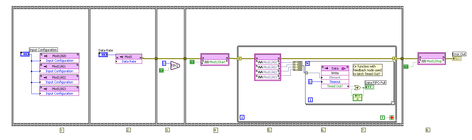
Below you will find my FPGA code before solving the problem and after resolution of the problem.
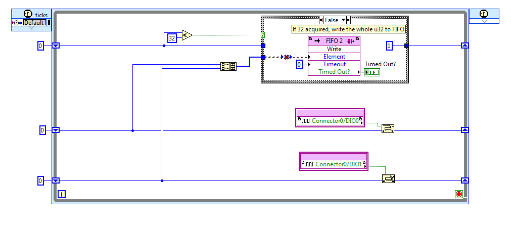
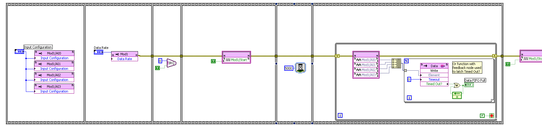
Solution: I just added a function of 5000 milliseconds (5 seconds) to wait before getting the analog input nodes samples (AI).
Before:
After:
-
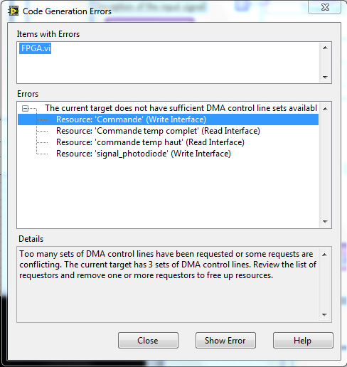
A Labview program with 4 DMA FIFO on FPGA card that can support DMA only 3
Hello
I am a beginner on LabVIEW FPGA, my internship that I work on the previous intern program, there during his internship and he published this program in its report.
On his program, it's that he put 4 DMA FIFO, but supported the FPGA (PXI of NOR-7951) map where we work me and the trainee takes only 3 DMA, so I can't run the program, I have this error:
I wonder if it's a bug or anything else, any ideas?
Sorry to answer the longer end, thank you for your response thank you for your help I could change my program, now the program run with three 3 DMA, I used a table to 2 signals in a single FIFO DMA.
I show the program, that can help someone with the same problem.
-
DMA FIFO of FPGA compilation error
Hello
I have a cRIO 9074 with FPGA. I tried a simple piece of code to learn how to acquire the data that is generated on the FPGA at a rate of 10 KHz and transfer it to the host VI to treat later in offline mode. However, I meet this compilation error when you compile the FPGA VI base containing a node to write FIFO (photo of the VI attached below). In compiling the report, it is said that there are 256 RAM Block used (the total number is 40), so an error has occurred. The error notification of exact compilation from Xilinx report is reproduced below:
# From the PAM program
# o toplevel_gen_map.ncd - intstyle xflow-calendar toplevel_gen.ngd map
toplevel_gen. FCP
#----------------------------------------------#
"Target part using" 3s2000fg456-4 ".
Design of mapping in the lut...
Guided running of packaging...
Running based on the delay of packaging of LUT...
ERROR
 ack:2310 - type compositions "RAMB16" too found to adapt to this device.
ERROR: card: 115 - the design is too large to fit the device. Please consult the Design summary section to see what resource requirements for your design exceeds the resources available in the device. Note that the number of slices don't notice it that their packaging could not be completed accurately.
NOTE: A file NCD will be always generated to allow you to examine the mapped design. This file is intended for evaluation use only and will not be processed successfully by means of BY.
Mapping performed.
See the report of map file "toplevel_gen_map.mrp" for more details.
Problem encountered during the packaging phase.
Summary of design
--------------
Error number: 2
Number of warnings: 125
ERROR: Xflow - card program returned the error 2 code. Aborting the workflow execution...
Bitstream not created
Time history analysis
What does that mean? How can I fix this error?
Thank you
Bogdan
Hey,.
Have you already tried to reduce the size of the FIFO memory?
Christian
-
Hello
can someone tell me how to stop Fifos DMA as a target host on the level of FPGA FIFO?
The node of the method 'stop Fifo' host only erases the fifo buffer on the host side. The Fpga FIFO is still running.
To reset the whole fpga is not possible, because the running code is important for control of the measure.
Thank you very much

Hi b.,.
you might stop to write in the FIFO with a Boolean control connected to a structure of matter...
-
Using TWO DMA FIFO target host
Hi, I use a unit 9004 cRIO for the purpose of data acquisition. I try to get signals analog (NI 9221) and CAN (NI 9853) modules and transfer them from the fpga VI VI in real time using DMA FIFO, that is to say, target to the host. I thought I should use 2 DMA FIFO, one for analog and CAN signals. When I tried to put them, I put the two FIFO in the same loop. I don't know if that's the only reason, but it would generate overflow error 50400. When I removed a FIFO and put the single FIFO, it worked fine. So, I thought they must perform independent while loops and implemented two while loops that would be run in parallel. And it worked. I don't know if this is how it is supposed to work? Is this that FIFO DMA should be run in parallel loops? Are they written in such a way that the FIFO function cannot be called for more of an instance in the same loop? This seems odd.
I should also mention that I reconnected it the wires on analog, digital and CAN modules before putting them in separate loops. And I know for a fact that the FIFO CAN show underflow error if the entry of the threads on the port CAN are not connected. Also, I don't use mode Scan Engine (I think that its not available in 9004)
You are right about the 9004 and Scan Engine - or the lack of support, I say... Regarding the error of underflow, this behavior is expected when you have two Scriptures DMA FIFO the same loop. What is happeing, it is that the two FIFOs write in true parallel. Thus, when you write to FIFO1, FIFO2 expected FIFO1 finish. Then, when you write to FIFO2, FIFO 1 must wait on FIFO2 and the while loop to reiterate before he can write more data. So, on your VI in real time, if you try to access one of these FIFO that has no data in there because it is waiting to write the next block of data, then an overflow error will happen.
When you separate the two FIFOs, both can run independently from each other and write at a much faster pace. In this way, your FIFO reads on the realtime VI will not be stuck in a State of negative overflow where a FIFO is waiting for data queued.
I hope this helps!
-
simple DMA FIFO reading two analog channels
Hello
I have a question on a method of data transfer between two analog inputs for a simple DMA FIFO in FPGA. The code is described here: http://decibel.ni.com/content/docs/DOC-6303. If I use this method, and I got out in a graph of my host VI, the calendar in the graph reflects the same schedule as the signals that have been entered? Or will they be phase shift between two signals?
Thank you
Grant
Grant:
Because it is not all information of timing with the signals in the FIFO, there will be no lag phase on the chart.
Hope that helps. I would like to know if I forgot something, or who does not explain very well.
Thank you!
-
Transmission of data to the host of RT to the FPGA via DMA FIFO
Hello
I try to write data from a host of RT on target FPGA using DMA FIFO and then process these data and read then return of the FPGA target to the host of the CR through an another DMA FIFO. I'm working on the NI SMU chassis 1062 q, with the built-in NI SMU-8130 RT controller and target FPGA NI SMU-7965R.
The problem I face is that I want to send three different tables, two of the same size and the third with different size, and I need one more small to be sent first to the FPGA. I tried to use encode dish with two executives in the FPGA VI. In the first image, I read and write the first table in a while loop which is finite (that is, a finite number of iterations). The second frame contains the process of reading and writing the second two tables (of the same size) in a while loop that can be finite or infinite (depending on a control). The problem is that it does not work. 2 arrays are displayed on the front panel of the RT VI host and works well, however, the table that should have been read in the first sequence does not appear on the front panel of the RT VI host. It is not sensible because if it is not passed from the host to the fpga and vice versa then the second image should not have been executed. Note that I'm wiring (-1) for the time-out period to block the while loop iterations until the passage of each item is completed. So the first while loop has only 3 iterations. Could someone help me undersdtand why this happens and how to fix this?
I enclose a picture of the host and the fpga vi.
Thank you.
If you vote for my idea here and it is implemented, you can even omit the loop FOR fully.

(I also propose the RE / IM divided inside the loop FOR and perform operations on complex table before the loop the transpose and reshape .) In this way, you only need one instance of these operations. You might even save some unnecessary allocations table in this way)
-
Use of FIFO memory on two areas of clock (Labview FPGA) block
Greetings!
I'm developing an application on the FPGA of the vector signal OR 5644R
transmitter/receiver. I have two loops single-cycle timed: a 40 MHz making a convolution
and writing a FIFO memory block and the second at 120 MHz (sample clock)
who reads from block FIFO memory and uses the following values
interpolation...Under what circumstances is it permissible to use a FIFO memory block to transfer
values of a loop from 40 MHz to a loop of 120 MHz (sample clock)?
The reason I ask the question, it is that the compilation of my code repeatedly of not
reported the error below:ERROR: HDLCompiler:69 - "/ opt/apps/NIFPGA/jobs/J9k7Gwc_WXxzSVD/Interface.vhd" line 193:
is not declared. I share for everyone's reference, screenshots of my code which is an extension of
sample 'Project streaming VST' given in NI5644R. A brief description of attachments is
given below...
1. "Top_level_FPGA_part1_modification.png": in a loop SCTL 120 MHz, a sub - vi bed FPGA
go a block FIFO memory... In fact, the reading is actually made when entry
"read_stream" is activated... (see details in read_from_fifo_true_case.png)
2. "Top_level_FPGA_part2_modification.png": a 40 MHz SCTL, wherein is a subvi FPGA
called to write the output of convolution to block FIFO memory.
3. "target_respone_fpga_block_FIFO_modification.png": an output of a convolution filter is
written in block FIFO memory each time that the convolution output is available...
'ReadBlockFIFO' VI (circled in Top_level_FPGA_part1) is invoked in a 120 MHz SCTL.
4. "read_from_fifo_false_case.png": when the input "read_stream' of this vi is false,
data transfer memory FIFO of block to a different FIFO ('generation filter") takes
place.
5. "read_from_fifo_true_case.png": when the "read_stream' is set to true, the data is read in
'Filter generation' FIFO and spent on the chain of later interpolation to the
120 MHz SCTL...
I hope that the attachments give enough clarity to what I'm doing... If we need
For more information, do not hesitate to ask...
Kind regards
S. Raja Kumar
Greetings!
I think I understand the problem... The error probably occurs because a DMA FIFO
(FPGA host) is playing at 40 MHz, and it is checked for the number of items in a loop
120 MHz... It is not captured by the "pre-processing" by the labview FPGA, but by the Xilinx
compilation phase synthesis tool.
A lesson I share, is that if you observe this kind of problem, watch if there is incompatibility
in the areas of the clock to access a FIFO...
Kind regards
S. Raja Kumar
-
Table sending via FIFO for xy charts
HI, I have data of sendig of evil from the FPGA to the UI of the host.
I want to draw 6 signals. on two XY Gratz, so for each XY graphs, I have 3 plots.
I have samples every 100µs on the FPGA and combine them into an array of 6 elements representing the values of y.
I send this table via DMA FIFO to the host.
On the host VI I devices the x values grouped into a cluster and build an array of 3 plots.
When I run the VI. I have a parcel of signals, but how the plots change all the time in another plot. Its like every time another element of the array is read. Until the current chart, I had only two plots and then it worked fine.
I hope someone can help me more.
As an attachment, you can find the FPGA VI, VI and VI of the host realtime
A few comments:
Looks like your axis x are evenly spaced (by 0.001) so you do not have an xy graph, but simply a waveform graph, which should simplify things.
I'm confused why you do your x-axis for Graphics1 to 100000 items long but just try to graph 30000 items in the feed. Similarly, for your graphics currents and Hall signals, it seems that the x-axis are long 4000 elements (although I have not your time - axis.vi to check) and want to 20000 graph items. Curve of waveform switching simplifies this.
When generating your table of 100000 elements you can simply use (i + 1) * 0.001 as output auto-indexée instead of using shift registers.
-
For a DMA FIFO running from the host to the 7976 is a data type that is optimum for PEP?
For transmission to the host 7976, I can pack my data in say U64s or break up in U8s. Y at - it a data type that will give the best rate? Maybe based on the bus (SMU) or the implementation of RIO drivers behind the scenes?
My experience is different. Once, I did a load of tests with different widths DMA FIFO for FPGA and tested the throughput and latency. If sending data via U8, U16 or U32 DMAs, I saw the same total transfer of bps. My explanation for this? Given that the width of the DMA is 32 - bit, LV little packaging in order to ensure that each part of the 32 bits is used. This means that if you have a DMA U8, it will transfer at a time, 4 to DMA 2 both U16 or U32 DMA one at a time. 64-bit is divided into two individual transfers.
Do not use FXP. Even a 1-bit FXP is represented internally as 64-bit and will require TWO DMA transfers to an FPGA.
Side fromt hat, U8, U16 or U32 makes essentially no difference because they are all packed 32-bit internally.
-
Reading and arraya thro DMA FIFO (PCI7813R)
Normal 0 21 false false false SL X-NONE X-NONE MicrosoftInternetExplorer4 / * Style Definitions * / table. MsoNormalTable {mso-style-name : « Navadna tabela » ; mso-tstyle-rowband-taille : 0 ; mso-tstyle-colband-taille : 0 ; mso-style-noshow:yes ; mso-style-priorité : 99 ; mso-style-qformat:yes ; mso-style-parent : » « ;" mso-rembourrage-alt : 0 cm 5.4pt cm 0 5.4pt ; mso-para-marge-haut : 0 cm ; mso-para-marge-droit : 0 cm ; mso-para-marge-bas : 10.0pt ; mso-para-marge-gauche : 0 cm ; ligne-hauteur : 115 % ; mso-pagination : widow-orphelin ; police-taille : 11.0pt ; famille de police : « Calibri », « sans-serif » ; mso-ascii-font-family : Calibri ; mso-ascii-theme-font : minor-latin ; mso-hansi-font-family : Calibri ; mso-hansi-theme-font : minor-latin ;}
Hello
Location:
I read 5-position encoder with PCI7813R. The position of encoder data format is I32. Following is each position encoder converted to U32 and build in a table by using "build the array function. Finally this table guided loop where I write it in DMA FIFO uses "FIFO write function. FIFO depth is equal to 16383 and Timeout to 0.
Side host I'm reading this table of DMA FIFO. The host FIFO depth is set to 1000000. I use 'Method Invoke with FIFO read' to read data from the FIFO. I read 10000 elements each time. Data output is converted to I32 and guided an extension to "decimate the 1 d array function. I use 5 indicators to represent the positions of Encoder on the host side.
And now the problem:
Position 1 Encoder shell displayed on indicator 1. But every time I close my application and run it again this position appears on the other indicator. Sometimes is the position of the Encoder 1 shown on the 1, sometimes on the indicator 5 indicator, sometimes on indicator 3... Although this position of the encoder is shown every time on the other indicator it has correct values. What I'll do as I will always receive encoder position 1 on indicator 1, position of the Encoder 2 Indicator 2...
My application has been built according to these instructions:
http://zone.NI.com/DevZone/CDA/tut/p/ID/4534
TNX,
Gregor
Normal 0 21 false false false SL X-NONE X-NONE / * Style Definitions * / table. MsoNormalTable {mso-style-name : « Navadna tabela » ; mso-tstyle-rowband-taille : 0 ; mso-tstyle-colband-taille : 0 ; mso-style-noshow:yes ; mso-style-priorité : 99 ; mso-style-qformat:yes ; mso-style-parent : » « ;" mso-rembourrage-alt : 0 cm 5.4pt cm 0 5.4pt ; mso-para-marge-haut : 0 cm ; mso-para-marge-droit : 0 cm ; mso-para-marge-bas : 10.0pt ; mso-para-marge-gauche : 0 cm ; ligne-hauteur : 115 % ; mso-pagination : widow-orphelin ; police-taille : 11.0pt ; famille de police : « Calibri », « sans-serif » ; mso-ascii-font-family : Calibri ; mso-ascii-theme-font : minor-latin ; mso-hansi-font-family : Calibri ; mso-hansi-theme-font : minor-latin ;}
Sorry Jochen, I placed the function reset at the end of my routine. L I corrected (put it on the beginning of the routine) and now it works as it is supposed to be.
Thanks a lot again!
Kind regards
Gregor
-
Number of DMA FIFO of items to read mismatch in the FPGA and RT
Hi all
I use myRIO, LV14 to run my application.
Request: I have to continuously acquire data via FPGA and host RT process once every 2000 samples are taken. I use DMA FIFO (size 8191) to acquire data, use timeout property in the FPGA to eliminate the buffer overflow. I had followed cRIOdevguide to implement this part. An excerpt of what I put in place is attached. All code runs in the SCTL at 50 MHz.
Question: Two or three times I met with this strange behavior, the FPGA FIFO gives continous timeout and the RT is unable to read the FIFO. The number of elements to set the property in the FPGA VI gives 0 showing that FIFO is full and no more can be written, but the RT, remaining items gives 0, so it is reading 0 (none) elements.
Solution: I put a case where I'll write to FIFO (under the code) and if the number of elements to write is different from zero. It seems to work fine, from now.
What confuses me, is that my FPGA VI said that FIFO is full (number of items to write 0 = FIFO) and gives a timeout error, but RT VI said that number of items remaining in the FIFO is 0 and therefore no data is read. No idea why this is so? My RT and FPGA VIs continues to run, but with no gains or to read data.
A few minutes after you run the code, I've seen this behavior. No idea why this happens? I try to reproduce the behavior, and will update if I meet with her again. Sorry, I can't post my code here, but I guess the code snippets to explain some extend.
Thank you
Arya
Edit: Even with the mentioned workaround solution, the problem persists, now that the FPGA written any of FIFO. And the RT VI is not able to read all the elements he sees 0 items in the FIFO. The FIFO continues to be in a State of timeout. So I guess that the problem is on the side of RT.
Why it looks like you read from the FIFO even in two different places in the same VI, at the same time? If the lower reading throws the FIFO, it will never trigger the reset, which could lead to the situation you describe, I think (it's hard to tell from a few screenshots).
Also, your logic seems too complicated. I immediately noticed that there is no reason to select the entry, the output of = 0 - simply use the 'equal to zero' output directly. On the side of FPGA, why you need check the number of items that you want to write? There's nothing wrong with writing in a FIFO that is already full. just the data won't get written.
-
SMU FlexRIO DMA FIFO host read the FIFO overflows broadband bandwidth/DMA issues
I'm working on an application that uses 2 modules FlexRIO, and 2 LVDS digital I/O adapters. I'm driving each of the SDC A/SDC B ports on LVDS 16-bit data at 50 MHz adapters. The FlexRIOs are expected to receive the data and write down them on four targets-to-host DMA FIFO (one per connector SDC), or two by FlexRIO. The host reads the FIFO and brings together a series of tables each FIFO output 2D. Ultimately, the individual tables (we're each a quarter of single image) will be assembled in simple images, but I haven't gotten that far yet.
The duty cycle for the data is about 80% (in other words, I'm only transmit data to the FlexRIOs 80% of the time, the rest of the time the transmitters are disabled), so the flow is about 80 Mbytes/sec/port total invasion, or 320 MB/s on the four FIFOs DMA. I find that the acquired data gaps sometimes inside that line up along the length of the material part of the DMA FIFO in FlexRIO modules. In other words, if my memory FIFO DMA are set to 65535 length, I'll see a break in the data acquired at the word of data 65536th. Data is a waveform of sight, which is essentially just a counter, so it's easy to see the break in the model. For the words of first 65535, adjoins the data, then from Word 65536 model is discontinuous and starts counting again from there, contiguously. At the beginning of the acquisition, the FIFO is erased: the beginning data read from the FIFO is always aligned correctly, so I know that the process starts at a good point.
The error is not always the case: sometimes I get continuous data through the point 65536. In addition, the error occurs independently between the four FIFO: on a particular race, a FIFO could have data of interest and some bad. Rarely, all four FIFOs have good data.
The fact that the gap of the configuration is to the point even the depth of the FIFO DMA tells me that fills the FlexRIO FIFO, the FPGA hardware without the system managing to move to read, which means that the data gets dropped during the period that the FIFO is full. Then transfer to the host comes into action, there again is the space in the FIFO, and the data is once more contiguous in FIFO memory for a large amount of data (I have not yet tried to locate a second gap in the data of a single acquisition). It seems therefore that the host doesn't have enough bandwidth between the FlexRIOs and the host of RAM to prevent the filling FIFO, or comes along some software process on the host that is temporarily stop the ability to instantly transfer.
Are at - it a specification for the SMU flow system that would indicate that we are trying to use too much bandwidth? Or are there priority controls on DMA FIFO that would allow us to raise the priority of the FIFO transfers as they are guaranteed to go in preference to other system tasks?
System Specs:
SMU-1075 chassis
SMU-8135 CPU
2 SMU-7962R FlexRIO modules
2 digital i/o modules of NOR-6585
LabView 2012 32-bit SP1 version 12.0.1
A suggestion of an applications engineer of NOR and some experimentation has solved the problem. It turns out that I was calling the method FIFO of DMA stop just before the outbreak of the transmission of the data via a control for the FPGA FPGA VI. I did this in order to clear the FIFO before you begin data acquisition, but I didn't know that this method disables also transfer data between the memory FlexRIO and host. Following this call, I trigger the FPGA code to start filling its FIFO and then begin reading. Calling the Read of FIFO of DMA apparently light up the transfer back, but it seems that the host VI has been randomly slow down enough to move to the bed such as filling the side FlexRIO FIFO and dat would be lost. I changed the host VI to insert a FIFO method call start before the trigger for the FPGA signal, and the problem is now gone.
Maybe you are looking for
-
How can I avoid that FaceTime opening automatically when I connect
Recently whenever I connect, FaceTime is active. I don't have it on my dock and does not know why he keeps coming back. Irritating to have to close every time I use my mac. All solutions?
-
I recently bought a macbook pro. Do I need to have an antivirus?
I recently bought a macbook pro. Do I need to have an antivirus?
-
Thickness of Lenovo IdeaPad Z500 HDD; Replacement of SSD
Hey guys,. I own a Z500 IdeaPad with a ST500LM012 HN-M500MBB 500 GB HDD by Samsung. I would like to do an upgrade with a 1 TB of HDD, I would put in the HARD Drive Caddy (replacement CD/DVD drive). And I also intend to get an EVO 840 Samsung SSD, I p
-
Where to find the additional templates as I have only the basic sounds of Windows now.
The selections of sound patterns, that I used to have love, but they "disappeared" after my recent restore/restart process. Can I get it for the installation of the sound patterns, such as space, Nature, & Leonardo da Vinci for free online?
-
Cannot access Smart WiFi in cascade mode
I have the following Setup. My modem ADSL ISP is the main router with DHCP and its address is 10.0.0.138 who, for some reason, I can't change. I booked 10.0.0.1 for my EA2700. My EA2700 Port 1 is connected to my wireless Internet service provider rou