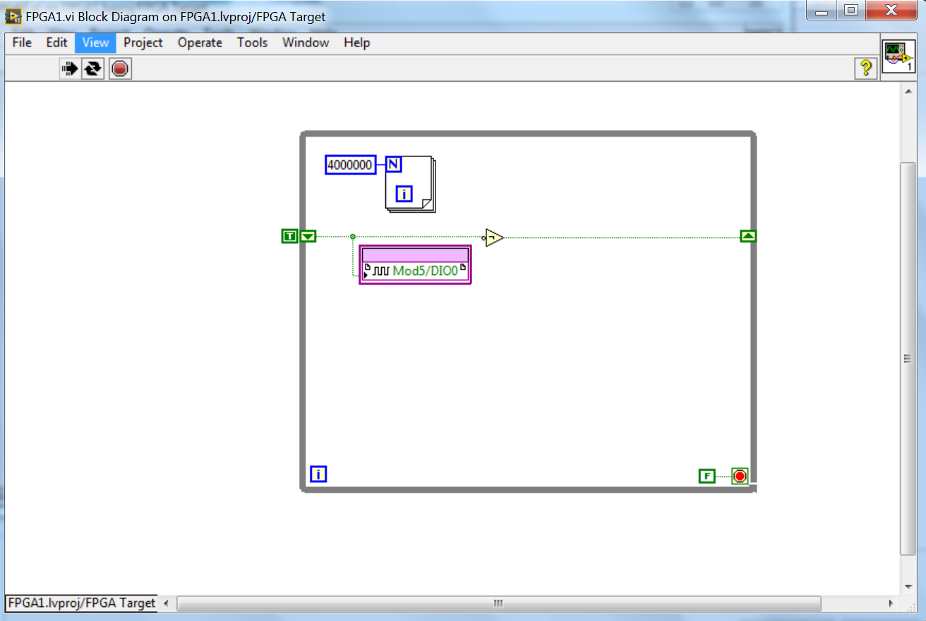
Digital speedometer on an FPGA
I'm trying to implement a simple digital tachometer on a machine. Its a proximity detector and a disc with several holes. I want to check the disk rotates and don't care (at least for now) how fast. I use a digital camera on my FPGA 9074 and just want to check for the transition to digital on a defined period of time. Can someone please show me where I can find a vi model that will accomplish this? Or does have a vi that they could share?
Thank you
Hello
Here's a DevZone with a link to the code example for the decoding of signals of tachometer. Sound using analog signals, but it should not be difficult to change analog signals into digital signals. Someone else on the forums perhaps implemented this with digital however.
See also the following Discussion forum.
Kind regards
Andrew
Tags: NI Software
Similar Questions
-
Laser digital lock with Labview FPGA?
Hello
Sorry to bother if you are not interested in this issue of digital signal processing. We are looking for a possible digital solutions to our problem locked frequency cavity closed-loop laser (see attached PDF file for more details). The goal is to flatten the PZTs transfer function (cancel the resonances and anti-resonances and their phase shift matching) in the frequency domain, in addition to the normal PID control. Input/output necessary voltage signals are small (we have our own amplifiers high power for the PZTs), and their bandwidth must be at least of 50 kHz (100 kHz would be optimal).
Among various OR hardware/software (DSP, FPGA, cRIO etc.), would anyone recommend a cost-effective solution for rapid prototyping?
Thank you!
I would like to look at the FPGA PXI cards nor 7854r. I rate of 750 kHz, 1 MHz AO. According to the involved treatment, you might expect between 200 and 750 kHz closed control loop. If the treatment is very intense, it's probably something less than 200 kHz.
That said, the key to these performance levels is not trivial and great care and attention to detail must be used in the coding of the FPGA.
Good luck
-
Digital FPGA of entry of the negative voltage
What is the maximum negative tension that the digital input on the FPGA can take without damaging it? I tried to look in the data sheet for the sRio 9636 and I can't.
Thank you
Hi, Berthe.
The sbRIO-9636 was DIO only on the OID (J502) and connectors MIO (J503). It's a bit different from the other variants sbRIO-96xx that others may have a RMC connector that has additional DIO.
Connectors IDC 50 pin DIO and MIO are 3.3V pins, but they are 5V tolerant inputs we have protection on the IDC DIO connector. VIL values and HIV are specified in the data sheet:
http://www.NI.com/PDF/manuals/373378d.PDF
These are the recommended conditions of use. If you need to know the maximum negative voltage to determine if your landing short of the runway is acceptable, this number to an absolute minimum is - 500 mV. I would recommend you choose the appropriate to your driver series termination resistors to minimize landing short of the runway, however. The absolute minimum even applies to the 3.3V RMC DIO as well.
-
exit node digital fpga Boolean realtime control
I have a system where I want to enable / disable a digital output running on FPGA.
Once I set the Boolean value on my side in real time (which turns out FPGA), I see the output turns on the CRIO, but it flickers on and OFF (do not lock?). I just want the FPGA to stay as long as the output is enabled, on the coast in real time. I can't change the mechanical action of the switch because of limitations on FPGA / RT according to labview (I get an error on compilation)
Any suggestions on how to fix this?
tman2013 wrote:
What I am doing wrong?
You reset the FPGA inside of the loop, in "Open FPGA Part.vi. You must open the FPGA reference once, outside the loop, instead of open it several times. Whenever you reset the FPGA VI, exits back to the default values.
-
myRio digital simple matter of e/s
This is probably the simplest question, you can get, but I have a requirement to the output of the digital output on the FPGA-say D0 pin on the port B. I use a switch for that and it works fine when I have a while loop with timer it contains. When I take off the whole loop and have the switch and the digital output on its own it doesn't work anymore. Why is it a while loop on this subject? the attached picture is when it works. Does not work then the while loop is deleted.
Hi tomnz,
What do you mean by "it doesn't work anymore? The loop allows the program to run continuously (when running, it will take the output command you give via the Boolean control), but otherwise the code runs only once.
-
digital output usb6009 does not switch does not correctly
Hello
I have a little problem with my 6009.
Basically, I switch the inputs of a Demux (74HC238D) (3 lines) write an address on it to select rows of data off the Demux.
The signal from the acquisition of data through an FPGA and the signal is displayed on the input pins Demux. That is the problem.
(It is worth noting that the FPGA is well programmed (coz if it was'nt then the signal would not get the demux in the first place.))
When I connect the inputs of the FPGA to 3 digital lines of data acquisition and scroll lines (turning each one WE and OFF), the signal appearing at the Demux pins is not a proper logic level. (the voltage I measured the scope is about. less than 1.1 V). For this reason I choose any line, Demux output will always be on the first channel and will not select the other channel.
I tried the same test 7 connect supply of 5V data acquisition (each line) and after having programmed the FPGA, the correct voltage level is available on the DEMUX pins. The problem occurs when I try to scroll through the entries via the software.
I'm not which is the cause. My belief is the acquisition of data.
What are your suggestions?
Thank you
Labmat
Hi Labmat,
The first thing that jumps out to me is the fact that you use these signals to interface with an FPGA. Outputs digital USB-6009 are 5V or 3.3V TTL and commonly FPGA i/o is 3.3V. Just to double-check, as FPGA did you use?
Q: When I connect the inputs of the FPGA to 3 digital lines of data acquisition and scroll lines (turning each one WE and OFF), the signal appearing at the Demux pins is not a proper logic level. (the voltage I measured the scope is about. less than 1.1 V). I tried the same test 7 connect supply of 5V data acquisition (each line) and after having programmed the FPGA, the correct voltage level is available on the DEMUX pins. The problem occurs when I try to scroll through the entries via the software.
A: This no doubt hits the nail on the head. First of all, I'd be inclined to not use program any software directly and instead use some of the tools for debugging I/O connectivity that come with the Driver NOR-DAQmx. You can get these from the measurement and Automation Explorer (MAX).
' ' ' ' 'Start-up' all programs ' National Instruments ' measurement and automation.
Expand the tree of devices and Interfaces in the left pane, and then select your USB-6009. Using the Test panels button on the right pane, you can quickly perform digital i/o with the device.
Our best bet is to first take a multimeter and see if we can measure the correct voltage is distributed by the correct pins on the USB-6009 case.
Now, by checking the box USB-6009 Datasheet, we can see that, on Page 17, there are a couple of different ways that we can configure the method by which the output signal is driven out of the unit; We have Drive open and active collector mode. It will assure you that since you are trying to send a signal to the FPGA, the unit must be set to active training mode, in order to generate signals from 0V to 3.3V . Output open collector allows the generation of signals from 0V to 5V . This can be done through property OR DAQmx nodes in LabVIEW.
In terms of current...
The + 5V line that you used for the FPGA Nailer is evaluated to 200 my. General DIO lines on the USB-6009 case can generate a current up to 8.5mA. This limitation fits the specifications of digital input of your FPGA?
-
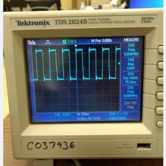
Can FPGA peak hold as the drawing attached.
The pulse of the Moose is all 0.3us wide. The scale of the hold of the tip is 20us.
The peak amplitude is 0.8V.
Thank you.
The faster module input analog cRIO is the 9201, that samples at 500 kHz, which equals 2 us intervals. It wouldn't be fast enough to take your pulse.
Fastest card of the R series is 750 kHz, which is still not fast enough.
If you've built a simple comparator circuit that would turn your pulse to a TTL level signal, you can connect to a digital input on the FPGA (probably R series only) and read pretty quickly. You can use this signal to activate an exit market and stop right analog time. It wouldn't exactly be a hold of the tip, but it would be close enough.
I hope to get an answer to your question.
Bruce
-
Fortunately the cRIO merger two time real screws: analog and digital output
Howdy,
I need help with a cRIO code. The purpose of the code is to acquire an analog input from the NI 9234 c series module and be able to send a "signal of pulse" digital camera (first low for some time, t1, then high for some time, t2) from a NI9401. Separately, I wrote the code to perform both tasks. However, when I add the code of RT digital output pulse pulses to analog input RT code, the DMA FIFO overflows because of the way that my digital pulse output code works. Currently, there are two reasons which overflows of the FIFO:
- The digital output code is pending for a while loop (pending "Send Pulse" become a true), the loop I can't empty the buffer FIFO
- The FIFO is not enough, quickly emptied depending on how long the pulse (t1 and t2) times are. The way I keep the pin high or low for a defined period of time is by issuing a sleep command, which blocks the loop I empty the FIFO. (Is there a "best" way to sleep?)
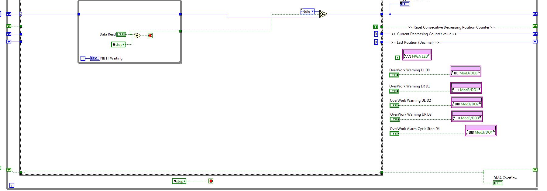
I have attached photos of my codes FPGA and RT. Please give me a suggestion on how to marry my two loops of RT for the use of happy resources! Thank you.
I found a quick way to solve this problem. I moved the timing of the Digital pulse on the FPGA. So whenever I have a Boolean value, the FPGA generates a waveform with the settings I put (a pulse in my case). This works because the FPGA loops run in parallel, I think. That's why, when I run a pending order in the loop of FPGA digital output, it does not prevent the FPGA of analog input loop to run. I have attached a picture of the code.
-
Do I need other Anti-Aliasing before resampling
Hi all
Just thinking how this resampling works.
Basically, it's just a standard resampling with dynamics of the frequency. This means he could the high frequency alias noise down in the region of interest.
The analog inputs have smoothing filters that will filter the signals to (-3dB) 24.56 kHz who works for the IO module because the nyquist frequency is 25 kHz.
However we then re - sample up to (for 50 Hz) rated 12.8 kHz. This means a nyquist of 6.4 kHz for everything from 6.4 to 24.56 kHz can alias downwards.
This can be solved by introducing a digital filter in the FPGA with a better cut-off frequency (to handle variation so probably want a bandwidth of at least 7.04 kHz 55 Hz) but I've not seen this in any of the examples.
Am I mistaken, or nobody ever bothered?
See you soon,.
James
Decided to take the experimental approach!
Generated a wave of 50 Hz with a 5% 10 kHz imposed on this topic and it doesn't come through.
Dig deeper into the resampling, there seems to be a FIR filter in it which I think is taking care of him.
See you soon,.
James
-
Digital electronics FPGA Board Hardware Driver for Windows 10
My son just made me aware that his school has a dozen of National Instruments Digital Electronics FPGA boards, but they have never been able to get them to work or actually use them in the curriculum. It seems that he has left his instructor know that I worked with FPGA Xilinx for more than 10 years and now everyone counting on me to get these maps work. The issue seems to be the USB driver. According to the manual, I tried DEFB2012_5_2.exe which simply refused to run on this machine Win 10 x 64. DEFB_4_3.exe ran, but complained that LabView components have not been installed and that it would not continue. Could someone tell me please how to install USB driver ONLY so that we can download files of bits with IMPACT? In terms of a school budget, the investment they have in these maps is not negligible. Thank you.
Hello Dave and TGregor,
I hope I can clear some things here. I'm sorry that you run in so many questions with your boards OF FPGA.
First of all, direct responses:
The LabVIEW FPGA 2015 driver should install the components needed to use the Board with Xilinx tools on WINDOWS 7, it will not work on any system more recent that the pilot has been developed before the release of Windows 8 and 10.
http://www.NI.com/download/NI-Digital-Electronics-FPGA-Board-driver-software-2015/5857/en/
My recommendation for Windows 8 or 10 is rather install Xilinx ISE you find on Xilinx website or on the downloads page OR:
https://www.Xilinx.com/products/design-tools/ISE-design-suite.html
http://www.NI.com/download/LabVIEW-FPGA-Module-2016/6231/en/
The difficulty that you face here is that tool Xilinx ISE is officially supported only on Windows 7 and below. So even though I think it will work (and it will move to the difference in the link of the above driver OF FPGA) for Windows 8 and 10, you can continue to deal with certain issues.
Now you are all looking to program the FPGA using an HDL, Multisim and LabVIEW? If you just use an HDL, you should be all set to go and in the dev environment, you had planned using the program. Circuit design of Multisim 'S simulation tool which includes a complete library of graphic digital components. A digital circuit can be built using the graphical logic gates in Multisim then downloaded directly on the FPGA without first having to learn VHDL or Verilog. It is quite popular among the logical classes digital introduction and we can help you by establishes that as well if you are interested.
For anyone else who might stumble upon this page, I want to make sure you are all aware that, while the Board of Directors OF FPGA is still supported and sold, it has been developed a number of years and has recently been replaced by the Council for development of the digital system (DSDB)that uses a 7020 architecting and has much periphrials more to the program than the FPGA OF. So I know that it is not useful for the current issue, but anyone looking for if they would like to buy more OF FPGA boards, I recommend watching the DSDB instead.
Thank you!
-
24 v digital signal of the event from the host to the fpga power on/off
Hello forums or
Sheet material
cRIO-9074
module or 9472 digital module 24 V output c series
To expand on the topic described,
I want to be able send a trigger to alarm the fpga digital 9472 out that lasts 30 seconds using the operating system time real clock time on the host computer
The way I approached this problem is that
In the loop where the event occurs, if the event trigger is defined then the fgv has a time stamp when the event occurred is sent.
In the loop that communicates with the control of fpga, I write to the control based on the condition that the difference of the current time checked and fgv time is 30 seconds or less, then it will send the value true, otherwise send fake and wait for the next occurrence of the event.
The main problem after implementation of this is that 9472 led does not turn off when the false value is sent to it.
cordially Mzamanstl
Timer Keeper SD is a FGV so that it is written for her, once the event occurs
So if the event occurs so timestamp is stored and then the difference of the timestamp result is<30>
then a true value will be sent to the module of 9472
So basically I want the light and I want to do the 24 v output for 30 seconds then turn off and wait for the next occurrence
I think the method that I test it with is not very good, because I realize other factors that may contribute to this problem, so I think I found another way to test
and I will try it but its will take time.
cordially Mzamanstl
-
FPGA CRio do not give good digital outputs
I'm working on a project with the compact RIO fpga. I tried following the youtube tutorials and written tutorial, but I get no similar results in scanning FPGA interface.
I have attached my project. Here's the signal that I get from the Basic VI, which is a digital IO defined as output in a while loop. Alongside this, there is a loop for fundamentally changing the frequency of the digital signal from the top down. But whatever number I put in the loop for, it gives me the same frequency.
My thought process goes like this: If the CRio has a processing time of 40 MHz to a loop that cycles 400 times should give me a swing of 100 kHz output, which is not any number, I put in.
Any help is appreciated.
Thank you.
LabVIEW is almost certainly that compile to loop out like dead code (nothing happens so LabVIEW gets rid of it). I advise to use the loop timer function if you are looking to change the frequency or put everything in a timed loop. All in a timed loop will execute a tick.
-
sbRIO-9631 digital inputs/outputs using e/s node FPGAS and FPGA of i/o method node
Hello, I'm trying to configure my SBRio-9631 for the first time. I try to use the on boards to inputs and digital outputs. The following code will work? This is a simple "read the entries, 'or' some inputs and pass ' exits." I have to add "E/s method nodes FPGA" between my 'FPGA of i/o nodes"to get"modes of State of sorting for the input and output lines? Also, I can't simulate/test it works, by adding 5 VDC at the entrances, and not have any source of voltage output. Thank you for your time.
Hey, Spex,.
I really, really appreciate your help. Your follow up information was exceptional.
Thanks again for your help and your time.
gjmm
-
Hi all
We have NI 9421 digital input and digital output NI 9472 Modules. We can run these modules into a VI under the 9073 cRIO chassis. While we have added the FPGA target under the same chassis, we cannot use the modules. We also install the scan engine.
How can we use FPGAS and i/o Modules at the same time?
Once you add a target FPGA in CompactRIO chassis, when you deploy the code, the cRIO is configured for the FPGA mode, which requires a bitfile compiled to connect with the C Series modules. Remove the target FPGA or changing the mode of chassis in the project and by redeploying must reconfigure the cRIO for scan Mode, which allows you to use the IO module directly from the RT VI.
For more information, see this post.
-
Entered digital high frequency to the FPGA could not be detected OK
Hello
We want to connect the CMOS camera with PCIe-7842R with SCB68 box to analyze the image in the FPGA. There are PCLK (pixel clock) signal (36 MHz) and 8 bits of data.
On the 1st, we write a test program to ensure that we can detect the PCLK correct which is attached as program.png. The program is very simple there is a loop timed with 80 MHz, which should be enough take 36 MHz signal. If the value of 8000 "Digital 2", we should have 3600 (+ -1) like "digital." The reason why we (+ -1) is that we have no synchronization, is supported in this test program. And we can get the right result in this configuration.
2nd part, connect us data to 8-bit on FPGA and we get a wrong result of PCLK. Even connect us only 1 bit (which is labeled as DIO1 program) data, the PCLK is disturbed, and we can't find out why. The configuration of the connector is attached as connector.jpg.
We tried to make 2 very distant digital signals, but are still not. We tried to change the cables connected between SCB68 and FPGA of SHC68-68-RDIO cable for SHC68-68-RMIO cable because we think she may have better armor. We have a better result but still bad.
Now, we put "Digital 2" 8000 and we have about 3400 ~ 3500 as 'digital."which is false.
Does anyone have advice or commands on this problem? I'm very appreciate your kind help.
Thank you.
Maybe you are looking for
-
Botton on toolbar fades in an out and tabs load slowly when opening up the blank tab
When you open a tab it slowly forward stretch his load. For toolbar buttons, you must click on them, and then they fade slowly and then disappear slowly. When you click on the button to display the bookmarks it loads instantly for the button options
-
After a one-hour FF starts using up to 1.6 GB of CPU
This has happened for a long time, but it's really annoying. I have to restart firefox all the time. If I don't it will just crash. The cpu usage goes up to 1.6 GB and be generally more then 2 tablets, it is really slow [even with the low use of the
-
My satellite P10 554 seems does not have a wireless network,Device Manager does not have any problem with the network card. I have dsl internet wired connection works without any problem. but laptop have wireless.Thank you for your advice
-
Is my week old Lenovo H50 dead?
Hello After working OK for a few days since my H50 Lenovo now seems dead. When I turn it on: I see the word Lenovo on the monitor and a small spinning wheel. After 10 seconds, the screen turns white for a few seconds. The Lenovo Word then reappears o
-
Several errors, CAPI2 event on 2 Vista Home Premium PC from July 11, 2010
IS this a Microsoft problem? Until today, my two PC has reported no problems with CAPI2 updates. July 11, 2010, I have CAPI2 errors as below. The manual download of the file and extraction, he said "the certificate trust list is not valid. The certif