E/s FPGA node
Hi, I was wondering if the next i/o FPGA node acquires Mod1/AI0 Mod1/AI1, AI2/Mod1 and Mod1/AI3 simultaneously.
I mean I don't know if they are at the same time or not.
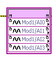
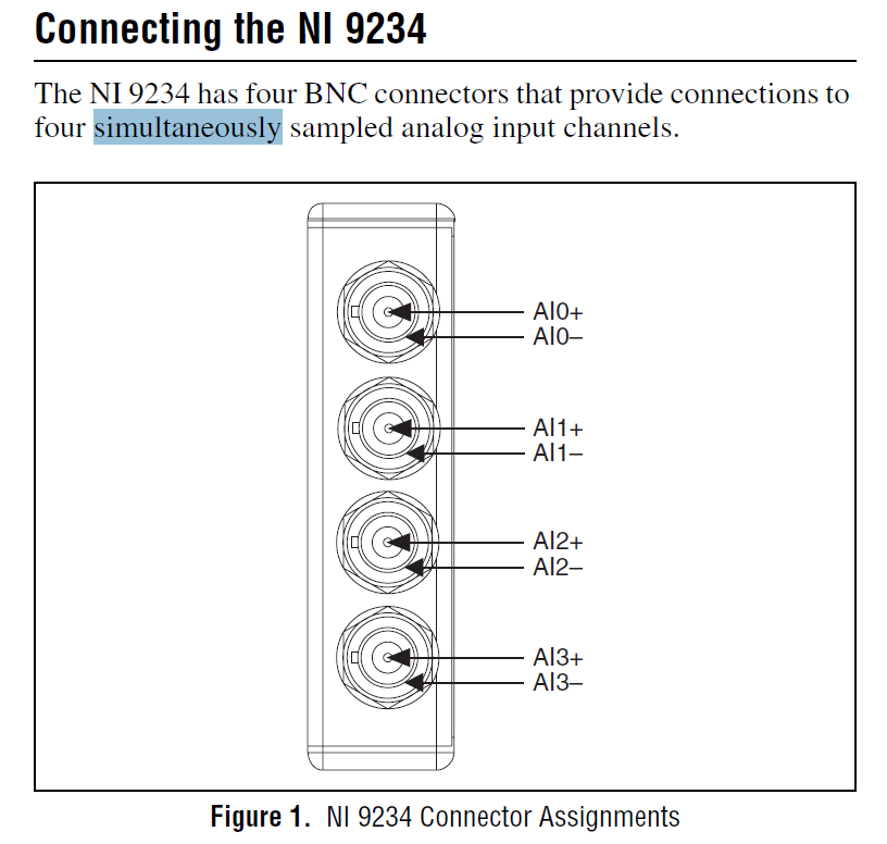
I checked the specifications of the NI 9234 module, as shown in the following figure.
As shown, for this module, all four channels are sampled simultaneously.
Now, I'm sure!
I think for each module, we should check the specifications to make sure.
Tags: NI Software
Similar Questions
-
Do not understand why "the node fpga Audio IN Terminal is 16-bit signed integer"?
Hello
I work with myRIO 1900 for my project of ANC.
Audio IN of the fpga node gives its type terminal data as integer signed 16-bit. So, finally the exit on the nodes of the fpga is fluctuating between two values - 1 and 1. But I want the actual values of the audio data, I did not understand how to address this problem.
Audio In on the side of RT gives type of terminal of data such as actual values, but I did not understand why the terminal of Audio In FPGAs is 16-bit integer. ??
Please help me solve this problem.
Thank you.
If your analog range of +/-2.5 V. 32768 then--would be the equivalent of-2.5 V. 32767 would be + 2, 5V.
If you get + /-1 V, then you should see somewhere between + / 13 107 on the analog input of the number I16.
Basically, take the n ° I16, divide by 32767, multiply by 2.5. You will have your analog input in volts.
I don't know why you thing it's just rounding up to the-1 to + 1. Something must be wrong with your code or configuration.
-
error 1136 When adding FPGA in SysDef
I have a PXI-7854R multifunction RIO installed in my SMU-1075 chassis. When I add it to the system under the FPGA node definition file, the RIO node is created with all its subnodes - as expected - but the attached dialog pop error. Whenever I highlight the node newly created Rio the same error appears. Everyone knows this?
I have an SMU - 6341 Multifunction DAQ designated as master hardware device Synch on the Bus 2 and moved to PXI_Trig0 through all three bus.
Also, I use Veristand 2011 SP1.
Thank you
Yes we have seen. Fortunately, it's just aesthetic. This happens when you have a DAQ master that is hidden in the tree and click devices FPGA. We hope to solve this problem in 2012. Sorry for the inconvenience
-
FPGA VeriStand personality is late? and latent FPGA data processing
I use a FPGA 7853 (only) in a SMU 1071 chassis with a controller 8135 and run VeriStand 2013 SP1. At the end of my test, I want to ensure the integrity of the test, which includes the audit of the FPGA interface is never late.
I first thought to expose the terminal 'Is?' late as a channel, but then I noticed it isn't really an account, it's just a flag. In addition, it seems that this flag is not locked, it does report by iteration of loop interface. This makes me think that I alarm an VeriStand on the later is for VeriStand FPGA interface design? channel. Am I correct, and if not, how NOR have I use East late? terminal?
As the DMA in the FPGA nodes then never expire, there no sense watching the Timed Out? terminals on the FPGA. But the effect of a timeout will appear in the East towards the end? Terminal Server. I'm tempted to change the end is? U64 to a real number in the number of late? the defined indicators synchronize to the host VI. is there a reason to not do this?
How VeriStand manages a FPGA end? If the RT side of the DMA buffer became more complete, data from the FPGA would be more latent, which could lead to the instability of the system. Hopefully the VeriStand engine should purge the latency of the data, but I don't see anything in the FPGA interface which would facilitate this.
Thanks for your help,
Steve K
Hey Steve,
If the PCL NIVS reads this flag as true, it incrememnts the County of HP system channel.
For the question of FIFO depth: The PCL is always expected to read and write a # fixed packages each iteration (as defined by the XML) and FPGA always reads and writes the same number of packets of each loop of comm iteartion and since the timeout is set to-1... orders may not be combined. Packets act as a handshake.
-
Terminal double knot of FPGA NI 9213
Hello
When I run the Sub - VI for the Started.lvproj get NI 9213, "NI 9213 Gettting Started (FPGA) .VI, get an error statitng that the FPGA node has duplicated the terminals. When I look at the terminals I don't see all those duplicate... I can't change this VI also. What could be causing this error and how can I solve it?
Thank you
Jose
Hi Jose,
You should be able to remove incorrect backplane of the project, and then you add in your basket under the cRIO controller. It is important that backplane in the project actually matches your hardware like FPGA chips are different in all of our basket funds.
Kind regards
Doug B
-
Try to compile some simple FPGA screws in my myRIO, but often get the error attached to the compiler. I got parts of vi works temporarily by manually of programming everything from scratch again (without copy - paste other vi), but now the simplest things (two while loops, one with e/s FPGA node with node of property of FPGA, stuff really really Basic) also give this error. This is getting frustrating. What I am doing wrong?
Best regards
Soeren
Hi new ppl
Now I came with a 'solution '. It turns out that if I create a new vi and manually (.. Yes manually) start placing blocks and make loops I can actually compile the FPGA vi. Sort of loops to copy - paste from one to the other vi makes a malfunction.
If someone else have experienced this?
.. .anyway to programming
Soeren
-
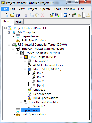
NEITHER 9870 on the NI 9144 NI 3110-controlled
I have the following Setup: A NI 3110 industrial controller acts as EtherCAT master. A NI 9144 slave is connected, having a single NI 9144 inserted in slot 1.
Can someone tell me please how to get this system running? I tried adjusting the NI 9870 examples with cRIO-90xx from the example with mechanisms DMA and interrupt but no job finder (I get lots of errors saying THAT DMA/interruptions are not available).
Any help is appreciated.
/ Christoph
Hi Christoph,
your system in the project should look like this.
The 9870 should be programmed into FPGA LV (using FPGA nodes as in the example of cRIO).
The issue is between 9144 and 3110, you can use DMA for transferas it data as happen using a simple cRIO system.
You must get your data in FPGA and the transfer to the controller using the user-defined variables as explained in the following link.
Getting started with distributed i/o systems deterministic
http://zone.NI.com/DevZone/CDA/tut/p/ID/7392
I hope it can help you.
Best regards
Andrea P.
-
I use a property of e/s FPGA node to get the serial number and the ID of the Module for each module in my cRIO-9081. The serial numbers match exactly what I thought, it was in my cRIO. The ID of the Module, however, makes no sense. I thought that the ID of the Module would have been 9201 for a module OR-9201. I got a number: 21754370963.
What should be the ID of the Module?
Hello Paul,
The module ID returned by the property ID of Module is not the name of the actual module (e.g. 9201). It returns an ID that you can then associate with a specific module as described in the link below.
C Series Module IDs:
http://zone.NI.com/reference/en-XX/help/370984R-01/criodevicehelp/module_ids/Kind regards
j_bou
-
I'm reasonably sure that all C series in a cRIO modules should be able to input/output simultaneous however, I want to confirm this and there are several models that not explicitly said in their data sheets. These models are the NI 9213 Thermocouple, NI 9402 and NI 9403 DIO cards. I guess they should all allow concurrent access on all channels, but I would rather confirm this with people who have used them before ordering devices.
Hi Michael,
I read your question in two different ways...
I CAN input and output at the same time on these modules?
The 9213 has no output, so it's a moot point. For the DIO 9402 and 9403 modules and most, then Yes, you can make entry and exit at the same time. You can confirm that open a project, add the module in the series C for a project, then go to the properties of this module. If you configure the channels separately, then Yes. Some modules to define both a whole port or module inputs/outputs, and these all would not O capabilities and I at the same time.
These modules sample at the same time?
Very few of our analog modules sample at the same time and they are usually called Dynamic Signal Acquisition (DSA) module - 9233, 9234, 9237 are examples. They have an ADC dedicated for each channel, so we can draw a measure of each of them at a time. Most of the other modules, as the 9213 you mentioned, have a single ADC and a multiplexer to analyze each of the channels one after the other, although very fast. So even if you can ask a FPGA node to read 8 channels both module, samples are actually slightly out of phase due to multiplexing. For digital modules, without multiplexing is required.
-
Detect voltage 9237 programmatically?
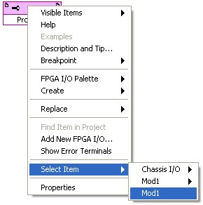
I'm using four 9237 complete Modules of bridge on a device of crio with interface FPGA and Labview 8.6. I'm trying to find a way to detect the voltage at runtime to include in the PDM file and be kept with the data. I was not able to find a way to do it. There seems to be no ownership of e/s FPGA option allows you to set or detect this side FPGA or RT of things. I find this curious because I feel that I should at least be able to know what properties and parameters the FPGA was compiled for.
Does anyone know how to do this?
Hello Rex 1030,
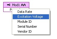
With a property of e/s FPGA node, you should be able to click on the node and select the 9237 Module as the property reference. See below for more details:
It does not appear that this property can be set to read directly from the module. If this property node should be implemented in the FPGA VI, FPGA Read/Write control could read the value set for the control assigned to the excitement on the FPGA target voltage.
Please report any additional question, if this process is not clear.
See you soon!
-
sbRIO-9631 digital inputs/outputs using e/s node FPGAS and FPGA of i/o method node
Hello, I'm trying to configure my SBRio-9631 for the first time. I try to use the on boards to inputs and digital outputs. The following code will work? This is a simple "read the entries, 'or' some inputs and pass ' exits." I have to add "E/s method nodes FPGA" between my 'FPGA of i/o nodes"to get"modes of State of sorting for the input and output lines? Also, I can't simulate/test it works, by adding 5 VDC at the entrances, and not have any source of voltage output. Thank you for your time.
Hey, Spex,.
I really, really appreciate your help. Your follow up information was exceptional.
Thanks again for your help and your time.
gjmm
-
FPGA IO node and loop Question of Timing
I'm having a lot of trouble to compile a very simple FPGA VI for a system for the acquisition of data on my cRIO (9075, using a single module 9205 cRIO, labview 2012 dev suite, xlinx13).
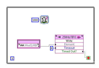
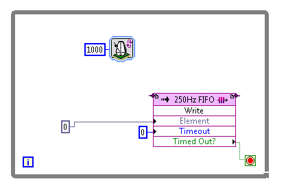
At the end of compilation, the error occurs if and only if I use a block of i/o node FPGA. This picture shows my very simple VI which fails to a compilation:
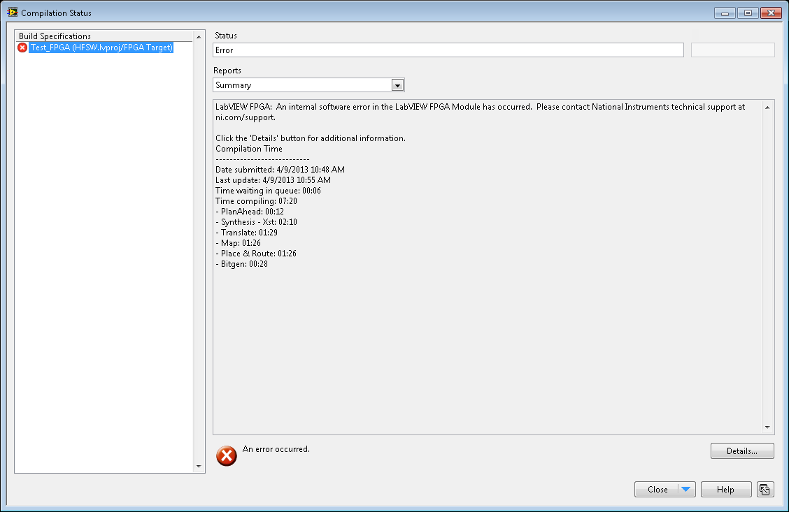
When I compile, I get this error at the end:
And here are the details of the error:
It is also interesting to note that the 'Timing' summary says I need a clock of 80 MHz, when the on-board clock of 40 MHz.
For comparison, when I remove the FPGA of e/s node and replace it with a constant, the compilation succeeds:
The need of a clock of 80 MHz disappears also, according to the report of timing.
Is this a problem with how loops work in FPGA? I've been reading about "single-cycle timed loops" that guarantee a performance per clock cycle. I don't have that kind of acquisition rate, and I guess the structure of loop, I created is not related to a single cycle because of the block of metronome, that I inserted. I guess correctly? Are there structures of loop for FPGA which is not related to a single clock cycle?
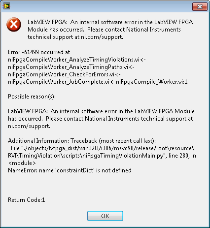
I also wonder if this error is not to do with my code, but is rather an internal error of the software compilation NOR, in particular the 'niFpgaTimingViolation.py' script mentioned in the summary of the detailed errors. I got labview 2011 and xlinx 12 installed on this computer before, but they uninstalled before the upgrade. This is my first project in 2012.
I appreciate the comments of the community NOR. Let me know if my question needs further clarification.
-Andrew
I solved the problem.
In case that someone looking for it later (error 61499 niFpgaTimingViolationMain.py that constraintdict is not defined).
I did a complete uninstall and reinstall my entire LV 2012 dev suite. Then the same VI used to compile failure began to pass compilation. Apparently, I had a corrupt file somewhere.
-
LabVIEW FPGA: Integration node clock wrong
Hello
I'm having some difficulties to understand how the clock is part of the node IP for LabVIEW FPGA and was hoping to get some advice.
What I try to do is to set up a digital logic circuit with a MUX feeding a parallel 8-bit shift register. I created the schema for this Xilinx ISE 12.4, put in place and can't seem to import the HDL code into an intellectual property node. When I run the VI, I am able to choose between the two entries for the MUX, load the output in the shift register, clearly the shift register and activate the CE.
My problem is that when I switch to the entrance of THIS, he should start 1 sec shift (Boolean true, SCR, High, what-have-you) in the registry once each clock period. Unfortunately, it instantly makes all 8 bits 1 s. I suspect it's a question of clock and here are some of the things I've tried:
-Specify the input clock while going through the process of configuring IP nodes.
-Adding an FPGA clock Constant as the timed loop.
-Remove the timed loop and just specifying the clock input (I'm not able to run the VI that I get an error that calls for a timed loop)
-Do not specify the clock to enter the Configuration of the IP node and wiring of the FPGA clock Constant to the clock input (I can't because the entry is generated as a Boolean).
-Remove an earlier version of the EC who had two entries up to a door and at ISE.
-Specify the CE in the process Configuration of the IP nodes.
-Not specify this in the process of setting up nodes IP and wiring it sperately.
-Various reconfigurations of the same thing that I don't remember.
I think I'm doing something wrong with the clock, and that's the problem I have. Previously, when I asked questions to the Board of Directors on the importation of ISE code in LabVIEW FPGA, a clock signal is not necessary and they advised me to just use a timed loop. Now, I need to use it but am unable to find an explanation online, as it is a node of intellectual property.
Any advice would be greatly appreciated, I'm working on a project that will require an understanding how to operate clocks the crux of intellectual property.
Thanks in advance,
Yusif Nurizade
P.S. I have attached my schematic ISE and the LabVIEW project with one of the incarnations of the VI. The site allow me to add as an attachment .vhd file, but if it would help I could just paste the body of the code VDHL so just let me know.
Hello Françoise,.
I spoke to the engineer OR this topic and it seems that it was sufficient to verify that your code works, by putting a wait function of 500 ms on the while loop to check that the registers responsible and clear. I'm glad that it worked very well!
-
Move from LabVIEW FPGA block of ram address to node CLIP?
Hello
I need to pass an index memory RAM of LabVIEW FPGA block to a CLIP node to the node CLIP to have access to the data in the BRAM. The node of the ELEMENT contains an IP address that we developed and the IP address is the use of Xilinx BRAM driver to access data. I guess that we need to move the physical address of the BRAM to the ELEMENT node.
Is this possible? If so, how? If this is not the case, what would be an alternative?
Thank you
Michel
If I understand you correctly, Yes, you should be able to use the memory block of the Xilinx pallet Builder in LabVIEW FPGA and in the loop of the single Cycle, connect the ports of this block signals CLIP exposed by the IP of your colleague. You may need to tweak/adapt some of the signals slightly to the LabVIEW data flow.
-
Integration of IP node: VHDL + LAVIEW FPGA
Dear members
can I use a library set by the user or a parcel inside the IP integration node?
for example library that contain a function for fixed operations in comma?
As
Library IEEE;
Use IEEE. STD_LOGIC_1164.ALL;Use mustafa... pkg
Unfortunately, there is no way to directly access a block of memory of LabVIEW FPGA and an IPIN node. You will need to file a read/write memory next to your IPIN node node and manage lines of coordinates and data of your IPIN node as ports.
Maybe you are looking for
-
In addition to messages on Flash Player that can be dangerous, when I click on the message I get redirected to the page about Java. I have the add-on Java last installed and active as well. I have not checked to see if this affects the content, but I
-
Acer Aspire One D270 does not turn on!
Have an Acer Aspire One D270. I've had for about 4-5 months now. Today it suddenly has stopped and it won't turn on. I left for a few hours but nothing yet. I thought it was a battery problem but the charging light does not turn. I know for sure, it
-
If you experience any of these issues, you can download and run the print and Scan doctor to help solve your problem.
-
Why can I not see a picture? n
I saved a picture in my "Images" file and I see an icon of the white page instead of the photo that I saved. I opened with Windows Photo Gallery and then could see the photo and I recorded it. The image still does not appear. Y at - there a trick
-
How to use PersistentBitmap in the version 5.0 or any other method?
I am completely unaware of an example of use of PersistentBitmap and am also not sure if it can be used in 5.0 but anyway, I extract the code next, I received, could someone advise me on how to use it? I have several images I want to stay put on the