Integration of IP node: VHDL + LAVIEW FPGA
Dear members
can I use a library set by the user or a parcel inside the IP integration node?
for example library that contain a function for fixed operations in comma?
As
Library IEEE;
Use IEEE. STD_LOGIC_1164.ALL;
Use mustafa... pkg
Unfortunately, there is no way to directly access a block of memory of LabVIEW FPGA and an IPIN node. You will need to file a read/write memory next to your IPIN node node and manage lines of coordinates and data of your IPIN node as ports.
Tags: NI Software
Similar Questions
-
Integration of IP node evil in LabVIEW FPGA
Hi all
I am having trouble with the integration of LabVIEW FPGA IP option and was hoping someone could shed some light here.
I use a simple VHDL code for a bit, 2: 1 MUX in order to familiarize themselves with the integration of IP for the LabVIEW FPGA.
In the IP properties of the context node, the syntax checking integration says:
ERROR: HDLParsers:813 - "C:/NIFPGA/iptemp/ipin482231194540D2B0CC68A8AF0F43AAED/TwoToOneOneBitMux.vhd", line 15. Enumerated value U is absent from the selection.
but I'm still able to compile. Once the node is made and connected, I get the arrow to run the VI but when I do, I get a build errors in Code Pop up that says:
The selected object is only supported inside the single-cycle Timed loop.
Place a single cycle timed loop around the object.
The selected object in question is my IP integration node.
I add a loop timed to the node, but even if I am able to run the VI, it nothing happens. the output does not illuminate regardless of the configuration.
I would say that I tried everything, but I can't imagine would be the problem might be at this point given that everything compiles and the code is so simple.
I have attached the VI both VHDL code. Please let me know if any problems occur following different boards of the FPGA.
Would be really grateful for the help,
Yusif Nurizade
Hey, Yusif,.
Looks that you enter in the loop timed Cycle and never, leave while the indicator of Output never actually is updated. Try a real constant of wiring to the break of the SCTL condition. Otherwise, you could spend all controls/indicators inside the SCTL and get rid of the outside while loop. You can race in the calendar of meeting bad in larger designs without pipeling or by optimizing the code if you take this approach, however.
-
Hi guys!
I am writing here after many days of attempts without success...
My request is 'simple', send data from the Panel of Labview RT within a DMA FIFO target host. Then the FPGA core receives data and imported through a knot of VHDL processes, and then after the data is pointing to the Labview RT through a target to host DMA FIFO.
I tested my node VHDL simulation mode in Labview FPGA where data sent by a target scope THAT FIFO and just work fine.
But when I try to run the node VHDL in the real target with data from the RT by DMA FIFO basis, it won't. I already do some checks:
-Data are properly sent through the host target DMA FIFO;
-The data are correctly received in the FPGA base;
-The data are correctly sent to the node VHDL;
-Result of the node VHDL are correctly sent to the heart of the RT through the target to host DMA FIFO;
-Result are correcly received in the heart of the RT, , but the result is false and absurd. But I have proof that my node is semanticly correct with my mock test
So my question: are there reasons to see my work VHDL nice knot in simulation mode and not in mode real target with data from the base RT by DMA FIFO taking into account data Transfer between DMA FIFO work well in both sides? Is there some sample available with data send RT FPGA-based via DMA and data processing with a knot of VHDL and returned to the RT kernel to inspire me?
I can't post my screw here because I work for a company, I use a MyRIO with Labview FPGA 2014 target.
Thank you guys! I am available for some details on my implementations.
Afghow.
Hey!
Thank you for your answer but I solved my problem. Indeed, at first, I tried to make a knot of Combinatorics (without clock) pure, but the problem seemed to come from that.
I modified my node in order to incorporate a clock, according to the prescriptions of this white paper: http://zone.ni.com/reference/en-XX/help/371599K-01/lvfpgaconcepts/ipin_prepare_ip/ . And now, every thing seems to work well.
The question remains why the combinatorial node has worked in simulation mode en not in the actual target?...
But for people with the same problem, I suggest add them a CLK and check an edge of entry with rising_edge (CLK) and if it does not, add an input signal to check if the input signals are valid or not.
Afghow.
-
Problem importing HDL node VHDL
Hi everyone, I'm using the HDL node in LabVIEW 8.6 for trying to import a VHDL design created using the of Matlab Simulink HDL coder. The problem I encounter is that design includes a state machine that HDL Coder created a separate VHDL file that the high-level VHDL to reference. At present, I found no way to tie the knot of HDL correctly this listing.
I have attached the files VHDL, both "as generated" by the HDL coder and a version that I modified to make it compatible with the HDL node (as for change of clk_enable to enable_in). The QEI.vhd is top level refers to the State in FSM.vhd machine. If someone could suggest a way to integrate the latter into the HDL node then it would really help my (very) limited VHDL.
Thank you
Andy
p.s. An idea that I think might work, but I'm not able to do (due to lack of knowledge of VHDL) would be to take the contents of FSM.vhd and include it in QEI.vhd. If someone could suggest a way to do that, then I'm pretty sure that would also solve the problem.
I managed to do a rather rough work-around to combine the two files that I'm pretty happy with for the time being.
-
What is the difference between abandonment and reset in Laview FPGA module
Hello
I used Abort in Labview FPGA e-mail trying to stop the running program in FlexRIO while I got an unexpected behavior.
After replacing the demolition of the reset all goes well.
What is the difference between these two functions?
Thank you
Fang
Hello Fang,
If this answers your questions, then please indicate that answers your question by clicking on "accept as a Solution.
If that doesn't answer your questions, so please let me know.
-
[Labview FPGA]: block of memory use Xilinx HDL integration node
Hello
In my project, I would be developed my own VHDL module and integrated in my project of LV FPGA with a knot of integration.
But for an evolution of my code, I wonder if it is possible to use in my own code VHDL, Xilinx library (as a block of memory).
Thank you.
You can use any Xilinx IP (or IP and others) in your external code. For example, if you generate a block of memory using block memory generator you can instantiate this IP in your own VHDL.
-
Do not understand why "the node fpga Audio IN Terminal is 16-bit signed integer"?
Hello
I work with myRIO 1900 for my project of ANC.
Audio IN of the fpga node gives its type terminal data as integer signed 16-bit. So, finally the exit on the nodes of the fpga is fluctuating between two values - 1 and 1. But I want the actual values of the audio data, I did not understand how to address this problem.
Audio In on the side of RT gives type of terminal of data such as actual values, but I did not understand why the terminal of Audio In FPGAs is 16-bit integer. ??
Please help me solve this problem.
Thank you.
If your analog range of +/-2.5 V. 32768 then--would be the equivalent of-2.5 V. 32767 would be + 2, 5V.
If you get + /-1 V, then you should see somewhere between + / 13 107 on the analog input of the number I16.
Basically, take the n ° I16, divide by 32767, multiply by 2.5. You will have your analog input in volts.
I don't know why you thing it's just rounding up to the-1 to + 1. Something must be wrong with your code or configuration.
-
Detection of contours in the HDL node
I used a knot of HDL to interface vhdl code in labview. The code should simply turn an led 'on' and 'off' when a button is pressed or relased, respectively. But when I run the code, the LED will remain off despite pressure on the button or not.
I'm not good in VHDL PROGRAMMIN but I need to demonstrate how to use the node VHDL to my presentation. Can someone help me with the button (or latch releasing proportionally) edge detection. ?
I use sb - RIO and Labview 8.6 FPGA module.
-
HDL is not showing node do not
Experience of other posts about it and have not yet understood what I am doing wrong. I can't find the node of HDL in an FPGA VI. I described the steps that I did below. Seems to me all FPGA modules installed as well. The only work around I could find was I open the sample project "with the help of HDL in Timed loop - R series' and copied and pasted the HDL of this VI block diagram node in mine. This seems to be a pain for what I want to do - anyone have any ideas on what could be the problem? Here are my Palette of programming to show you what I see:
STEPS TO FOLLOW:
- Create the empty project
- Right-click on my computer and select new-> objectives and devices...
- Click new target or device and select FlexRIO-> SMU-7966R
- Right-click on the FPGA target and choose new-> VI
- On the block schema do a right click and search for "HDL" or just look at the programming for Advanced-> HDL node Palette
Thank you
Bill
Hi Bill,
What version of LabVIEW are you using? The crux of HDL is obsolete for many years now, and thats why he is more so on the pallets. To import the external IP address, we now recommend the integration of IP node (IPIN) or component-level IP (CLIP). For your information, a valuable information on how to use each can be found in the Help of LabVIEW FPGA.
I DO NOT recommend that you use the HDL node for all new code development. The reason for which he still works, it's that support us because it is about so that we don't break upgraded code. If you absolutely must have the support of your application, you can do the following:
- In LabVIEW, go to Tools > advanced > Edit Palette put in...
- In the palette Editor window, select the palette you want than the HDL node to appear (I recommend Favorites, but what you are comfortable with is fine)
- Right-click and select Insert > VI (s)
- In the window that appears, switch to show all files
- Go to the browser window "C:\Program Files (x 86) \National 2012\vi.lib\rvi\HDLNode" or equivalent for your computer
- Select "nirviHDLNode.xnode", and then click Open
- Save your changes to the palette
Yet once, a continuous development with the HDL node is not recommended, and the API has been deprecated for several years now.
-
[FPGA] Question on the test on dev computer
I have an FPGA vi which I want to test on my development computer with the method presented here:
http://zone.NI.com/reference/en-XX/help/371599G-01/lvfpgaconcepts/test_bench_tutorial/
Very well so far, but a problem - the "custom FPGA of e/s" is actually replace my host VI if I understand correctly, but as well as simply to write data in the nodes of the FPGA, the host VI contains also some functions (not written by me but by NEITHER) who are called upon to interact with the FPGA vi and implemented. Is there any way I can call him these screws as I would on the host and have their place FPGA code when it running in mode of simulation on PC, or do I have to do something more intelligent?
Hi ToeCutter,
What kind of format are functions to your host vi?
The best way to call these vi of while still using the testbed would probably be to add automated execution host (described at the end of the document) vi, either before, during or after the while loop, according to their functions.
-
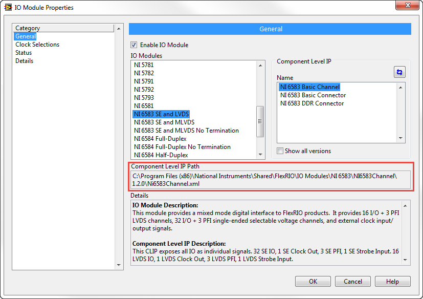
Hello
I am currently using SMU-7966R with module of e/s-6583.
For my application, I need to access IO with imported vhdl design FPGAS. As a result, I try to use a CLIP half bridge.
Following the tutorial process NOR, I imported a CLIP half-bridge (for example Ni6583ConnectorDdr.xml). But I can't find a way to instantiate this CLIP I heard the message:
"This statement of the CLIP is a CLIP half bridge and it cannot be instantiated in a socket."
Documentation OR I haven't found example for customizable CLIP but not how instantiate a socket, and then a half-bridge CLIP. You can define more precisely this procedure?
Thanks in advance,
Roman C
Hi Roman,.
To CLIP half bridge, it means that it must replace one of the sections CLIP material in the project, in this case the module. This means that when you choose which module you are using, you choose your CLIP instead.
I think that he can come in the entry, it must be stored in the right place on the disk to appear in lists in the dialog box. You can see the path of the existing CLIPs from the dialog box:
See you soon,.
James
-
Strange problem with my FPGA Code
Hello
I am running the following program, but I am facing a strange problem:
-I can read all analog and digital input and write on the outputs analog (I measure the tension that I write on the map of the AO)- But the valves I have connected to the analog output, flashes a red light (which, according to the data, sheet means the electrical signal I send to them via the module AO is incorrect)
-However, if I delete the ms and RMS block and do not make any average samples, but let all even (still two loops and two of the nodes separated from FPGA to e/s), the valves are operational and flash not a red light.
I have a cRIO with four modules:
-1. The (Mod1) AO cards
-2. Map of HAVE it (2)
-3. DI/O card (Mod 3)
-4. Map to HAVE secondary (Mod4)I currently have two loops on the fpga all-in:
-' Hand Loop (ML)': reads and writes I/O cards 1-3, with an expectation to 300us
-'Top pressure sensors Loop (PACKAGE)' reads two HAVE the fourth module (Mod4), with no waitingThese two loops are indicated in "fpga - part 1.png" and "fpga - part 2.png".
The settings for the ms and RMS measures VI, as well as the façade are indicated in "fpga - part 3.png".
The second loop uses 12002 ticks to run, the first loop use 160 ticks to run
Previously, I had a similar problem which was fixed by setting the initial values indicated on the front cover for the analog output to the valves.
Currently, I have not any target VI race and I'm only using fpga VI
Any suggestions? Thank you!
-
Installation integration broker
Hello
I'm trying to implement messaging between two systems HRMS 8.9 with the version of the tools for both being 8.48
I have a service operation is trying to generate a message on a fieldchange event. Routing out this service received:
the sender node: PSFT_LOCAL
Receiver node: TARGETNODE
the connector used for nodes that the above is PSFTTARGET (delivered connector)
On the bridge, when I try to ping the nodes, PSFT_LOCAL ping is successful;
However, by trying to ping TARGETNODE, it gives the following error:
Service integration Broker: Destination node does not match the local node. (158 506) +
This exact error is also received when I try to generate messages through the fieldchange peoplecode as well.
appreciate any input!
VikasIt should at least contain your fixed IP address also localhost servername directive.
Nicolas.
-
Xilinx Coregen does not appear in the palette
I would like to you can generate FIFO for my LabVIEW FPGA Xilinx Coregen project. The help file says to look on the palette of programming within an FPGA VI, but I did not. I have the node IP integration and all the functions the FPGA but not Coregen. The application itself is installed on my computer. Is there an installation option that I missed? How can I get this appears?
Rgds,
Nick
The .ngc file IS the netlist. It must be built next to the file .xco in the process of Coregen. It must have the same name (for mine, I named the generated_fifo component) If you want to see generated_fifo.xco, generated_fifo.ngc, and there should also be a generated_fifo.vhd. The .xco file is essentially a list of coefficients and build the basic settings. The .ngc file is a synthesized version of the kernel that used the file .xco for the generation. The .vhd file is a simulation of the core model. Usually, it won't not synthesized, but can be used for the simulation.
Thus, the only file you need to add in the configuration of the node would be the .ngc file (which is the netlist). You will then need to configure the behavior of simulation to use the corresponding simulation .vhd file or use a post-synthese model.
-
Target to host DMA FIFO - actual number of items
Hello
I have a target of FIFO of DMA host using memory block. Under FIFO properties, "the actual number of elements" is indicated as part of 1023.
But when I wire a remaining indicator to the 'elements' of FIFO in the host of VI, said 16384 elements. And I read a lot of part of the FIFO.
Why is the actual number of items that much more?
The data type is 32. And I have a high-7965R FPGA.
See you soon.
There are two different buffers for the FIFO: one on the host, the other on the FPGA. Data is copied from one to the other. It may be more space allocated on the host, because there are more memory available here and the loop of the host, probably runs more slowly than the FPGA. You can set the host using a node to invoke FPGA FIFO set the buffer size value.

Maybe you are looking for
-
How to import vcards to iCloud con contacts in outlook
Given that Microsoft has decided to stop using iCloud for office, how can I get my contacts to iCloud to Outlook on my pc?
-
I always get the error message E and empty flashing cartridge light after installing new black cartridge.
-
I finished the installation of a new KDL60EX701 TV and the network adapter USB UWA-BR100 to connect to my network wireless home successfully. As noted, I went to the network icon to activate the features improved and found my registration code. Yet o
-
PIXMA MX882 stopped scanning on WiFi
I have a printer all-in-one PIXMA MX882 worked as a champion of the last of the last years until I had to have my hard drive erased and a new operating system installed (long story). I re-installed the printer software and drivers (including the new
-
HP Officejet Pro 6830: How can I turn off Auto Save function before printing
I recently bought a new printer HP 6530 and configured using the wizard. Now whenever I try to print anything it forces me to save as a PDF doc before printing. I checked my settings and there is no 'save the doc' feature in advanced features. How