FPGA: IO node
Under my FPGA target, I have a module 9485. I have all 8 channels in my project, and I have a channel called 'CH7:0 '. ». What is c? I guess I can choose anyone of the channl with whom? How to use it?
It's the U8 integer you want to write for all bits 0 to 7 channels at the same time. For example, to activate all the bits, you must write 255 which corresponds to FF hex and binary 1111 1111.
Tags: NI Software
Similar Questions
-
FPGA IO node and loop Question of Timing
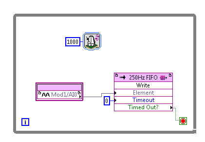
I'm having a lot of trouble to compile a very simple FPGA VI for a system for the acquisition of data on my cRIO (9075, using a single module 9205 cRIO, labview 2012 dev suite, xlinx13).
At the end of compilation, the error occurs if and only if I use a block of i/o node FPGA. This picture shows my very simple VI which fails to a compilation:
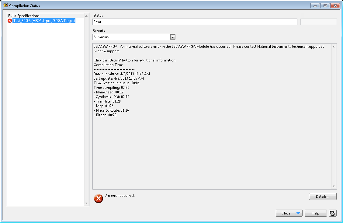
When I compile, I get this error at the end:
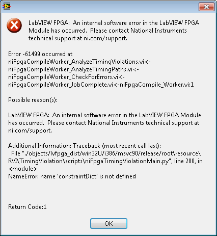
And here are the details of the error:
It is also interesting to note that the 'Timing' summary says I need a clock of 80 MHz, when the on-board clock of 40 MHz.
For comparison, when I remove the FPGA of e/s node and replace it with a constant, the compilation succeeds:
The need of a clock of 80 MHz disappears also, according to the report of timing.
Is this a problem with how loops work in FPGA? I've been reading about "single-cycle timed loops" that guarantee a performance per clock cycle. I don't have that kind of acquisition rate, and I guess the structure of loop, I created is not related to a single cycle because of the block of metronome, that I inserted. I guess correctly? Are there structures of loop for FPGA which is not related to a single clock cycle?
I also wonder if this error is not to do with my code, but is rather an internal error of the software compilation NOR, in particular the 'niFpgaTimingViolation.py' script mentioned in the summary of the detailed errors. I got labview 2011 and xlinx 12 installed on this computer before, but they uninstalled before the upgrade. This is my first project in 2012.
I appreciate the comments of the community NOR. Let me know if my question needs further clarification.
-Andrew
I solved the problem.
In case that someone looking for it later (error 61499 niFpgaTimingViolationMain.py that constraintdict is not defined).
I did a complete uninstall and reinstall my entire LV 2012 dev suite. Then the same VI used to compile failure began to pass compilation. Apparently, I had a corrupt file somewhere.
-
LabVIEW FPGA: Integration node clock wrong
Hello
I'm having some difficulties to understand how the clock is part of the node IP for LabVIEW FPGA and was hoping to get some advice.
What I try to do is to set up a digital logic circuit with a MUX feeding a parallel 8-bit shift register. I created the schema for this Xilinx ISE 12.4, put in place and can't seem to import the HDL code into an intellectual property node. When I run the VI, I am able to choose between the two entries for the MUX, load the output in the shift register, clearly the shift register and activate the CE.
My problem is that when I switch to the entrance of THIS, he should start 1 sec shift (Boolean true, SCR, High, what-have-you) in the registry once each clock period. Unfortunately, it instantly makes all 8 bits 1 s. I suspect it's a question of clock and here are some of the things I've tried:
-Specify the input clock while going through the process of configuring IP nodes.
-Adding an FPGA clock Constant as the timed loop.
-Remove the timed loop and just specifying the clock input (I'm not able to run the VI that I get an error that calls for a timed loop)
-Do not specify the clock to enter the Configuration of the IP node and wiring of the FPGA clock Constant to the clock input (I can't because the entry is generated as a Boolean).
-Remove an earlier version of the EC who had two entries up to a door and at ISE.
-Specify the CE in the process Configuration of the IP nodes.
-Not specify this in the process of setting up nodes IP and wiring it sperately.
-Various reconfigurations of the same thing that I don't remember.
I think I'm doing something wrong with the clock, and that's the problem I have. Previously, when I asked questions to the Board of Directors on the importation of ISE code in LabVIEW FPGA, a clock signal is not necessary and they advised me to just use a timed loop. Now, I need to use it but am unable to find an explanation online, as it is a node of intellectual property.
Any advice would be greatly appreciated, I'm working on a project that will require an understanding how to operate clocks the crux of intellectual property.
Thanks in advance,
Yusif Nurizade
P.S. I have attached my schematic ISE and the LabVIEW project with one of the incarnations of the VI. The site allow me to add as an attachment .vhd file, but if it would help I could just paste the body of the code VDHL so just let me know.
Hello Françoise,.
I spoke to the engineer OR this topic and it seems that it was sufficient to verify that your code works, by putting a wait function of 500 ms on the while loop to check that the registers responsible and clear. I'm glad that it worked very well!
-
LabVIEW FPGA CLIP node compilation error
Hello NO,.
I work on an application for my Single-Board RIO (sbRIO-9601) and faced with a compile error when I try to compile my FPGA personality via the ELEMENT node. I have two .vhd files that I declare in my .xml file and all at this point works great. I add the IP-level component to my project and then drag it to the VI I created under my FPGA.
Within the FPGA personality, I essentially have to add some constants on the indicators and entries CLIP to my CLIP out and attempt to save/compile. With this simple configuration, I met a compilation error (ERROR: MapLib:820 - symbol LUT4... see report filling for details on which signals were cut). If I go back to my VI and delete indicators on the output (making the output pin of the CLIP connected to nothing), compiles fine.
I've included screenshots, VHDL and LV project files. What could be causing an indicator of the output of my VI to force compilation errors?
Otherwise that it is attached to the output ELEMENT, a successful compilation...
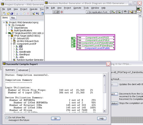
After that the output indicator comes with CLIP, compilation to fail...

NEITHER sbRIO-9601
LabVIEW 8.6.0
LabVIEW FPGA
Windows XP (32-bit, English)
No conflicting background process (not Google desktop, etc.).Usually a "trimming" error gives to think that there are a few missing IP. Often, a CLIP source file is missing or the path specified in the XML file is incorrect.
In your case I believe that there is an error in the XML declaration:
1.0
RandomNumberGenerator
urng_n11213_w36dp_t4_p89.vhd
fifo2.vhd
This indicates LV FPGA to expect a higher level entity called "RandomNumberGenerator" defined in one of two VHDL files. However, I couldn't see this entity in one of two files. If urng_n11213_w36dp_t4_p89 is the top-level entity, edit the XML to instead set the HDLName tag as follows:
urng_n11213_w36dp_t4_p89 Also - in your XML, you set the 'oBits' music VIDEO for output as a U32, however the VHDL port is defined as a vector of bits 89:
oBits: out std_logic_vector (89-1 downto 0)
These definitions must match and the maximum size of the vector CLIP IO is 32, so you have to break your oBits in three exits U32 output. I have added the ports and changed your logic of assignment as follows:
oBits1(31 downto 0)<= srcs(31="" downto="">
oBits2(31 downto 0)<= srcs(63="" downto="">
oBits3(31 downto 0)<= "0000000"="" &="" srcs(88="" downto="">Both of these changes resulted in a successful compilation.
Note: The only compiler errors when you add the flag because otherwise your CUTTING code is optimized design. If the IP is instantiated in a design, but nothing is connected to its output, it consumes all logic? Most of the time the FPGA compiler is smart enough to get it out.
-
Broken thread - FPGA Interface Node error
Hello
I am programming my application of RT and I get this weird error:
As you can see, I'm trying to set the value of a FPGA control (which is a typedef enum) and I get this strange cut wire
for me, error.
I was looking for a solution in the forums but I luckily able to get a... Could someone help me?
Thank you!!
PS: The error message was "the type of sink is zero" that is false, as already defined in the FPGA vi.
Solved.
To the right, it was like if I've changed some of typedefs and who did not have in mind. Recompiling solved the problem.
-
Pin configuration of e/s for an FPGA
Hello
I have a 7830R FPGA which has "DIO" pin on this subject. I would like to cofigure some of these pins to be entered and others to be taken out. Where to define what they must be configured as?
Cheers, AlecThere's FPGA IO nodes property that you can use to "activate the output.
-
I have a PCI-7833R. The FPGA is programmed so that it would provide two digital high constantly. We had a power outage and the FPGA was forced to power down. When I turn on the power, the FPGA provided is no longer the digital high two. I have the following questions:
-It seems to me that the FPGA VI did not at all after power off. The FPGA should not always run?
-For example, I have a new FPGA, and I run an application with bit, VI and VI FPGA host files. After that, I let the FPGA headlessly tracks. I guess that the FPGA has taken on the personality of the bit file of the application that I ran before. If this is the case, what part of the application he associated the file bit for the FPGA?
-If I don't have in my LabVIEW FPGA module and I get a bit of my colleague file, how can I associate the file bit my FPGA and FPGA works headlessly?
-After what a FPGA is configured with the personality of a bit file, what are all the means to clear that or corrupt that?
-If I have an FPGA that is running headlessly, and I want to do a reset, so that the FPGA runs again from the beginning. Is power cycle an option for this? Are there other options? Can I reset an FPGA without power cycling it?
Thank you!
jyang72211 wrote:
-It seems to me that the FPGA VI did not at all after power off. The FPGA should not always run?
N ° the FPGA loses its configuration when it loses its power and must be recharged again. In most of the FPGA systems (not just NO), this is done by keeping a copy of the configuration in an EEPROM or similar and load at startup. Some FPGA OR cards allow you to download a bitfile to flash memory built-in so that it will be loaded at startup, see downloading an FPGA VI to the Flash of a target FPGA.
jyang72211 wrote:
-For example, I have a new FPGA, and I run an application with bit, VI and VI FPGA host files. After that, I let the FPGA headlessly tracks. I guess that the FPGA has taken on the personality of the bit file of the application that I ran before. If this is the case, what part of the application he associated the file bit for the FPGA?
I don't know what you're asking here. Within your program of LabVIEW you specifically load a bitfile on the FPGA and run. You can also stop the FPGA and load a new bitfile within the same host application - this is useful when you want to perform several tasks without overlapping on the FPGA and there is not enough space to fit all of them in the same design.
jyang72211 wrote:
-If I don't have in my LabVIEW FPGA module and I get a bit of my colleague file, how can I associate the file bit my FPGA and FPGA works headlessly?
See "using LabVIEW FPGA Interface without the FPGA Module". When you do headlessly, you mean with no applications running at once, LabVIEW or something else?
jyang72211 wrote:
-After what a FPGA is configured with the personality of a bit file, what are all the means to clear that or corrupt that?
-If I have an FPGA that is running headlessly, and I want to do a reset, so that the FPGA runs again from the beginning. Is power cycle an option for this? Are there other options? Can I reset an FPGA without power cycling it?
There is LabVIEW FPGA method nodes to abort and reset the FPGA, so you can write a simple LabVIEW application for this. I can't say that's the only way, but it's the only one I know. I don't know of anyway to clear the FPGA without turning off, but the reset method can be close enough.
-
writing in an array of FPGAs for application of the rt
When you use the control to write in an application of rt to write to a table fixed fpga is it requires to perfectly fit the sizes of battery? I am assuming that you can write an array which is less than or equal to the size of table fixed fpga with no penalty.
You can write any table size to the FPGA IO node; It will be resized to the correct length. If you write a shorter range, however, I don't know if the remaining elements will be filled with 0 or something else.
-
I want to use some of my modules in scan mode and others in the FPGA mode. Although I could create a hybrid project, I can't do a VI implementation of two of them. I get an error as in the diagram I have attached. I want to read the analog inputs using NI 9239 scan interface mode and put out through 9269 mode of fpga. Is this possible? I'm kinda new to this.
Thanks in advance!
Of course, you can do what you were trying to here. You must at least two screws for this application. You will need a VI running under the FPGA target who can read and write the purple (FPGA IO nodes) nodes. You will need a VI running under the controller RT who can read and write variables, like the yellow node in your image. To talk between two screws, use the palette FPGA Interface to read and write controls and indicators on your FPGA VI of your RT VI.
This information gets you take off a little at the moment?
-
MicroBlaze soft core with Spartan-3F kit
Hello guys,.
Is it possible to implement a Microblaze soft core with kit-LABVIEW FPGA and Spartan-3E? Examples?
In addition, examples of executing a Picoblaze soft-core on Spartan-3E and using LabVIEW FPGA CLIP node kit? Thanks in advance!
This link points to a generation on the Virtex 5 FPGA platform. In principle, the process is the same for Spartan...
-
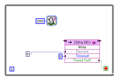
Target to host DMA FIFO not compensation when they are arrested
I use a PXI-7841R (Virtex5) and 32-bit data to the host via DMA FIFO transfer. When you read the FIFO on the host for the first time, the data are "stale" (which means that it is not what is currently coming in the FPGA, but what came in a few seconds ago stale). I tried both a stop and a configuration for clear memory FIFO before I use them. Documentation on one or both of these so-called clears the target and host the FIFOs. Does not help in both cases. With readings of the second and the following, FIFO has then 'valid' (same data as it appears on the FPGA entry node). What is curious is that each reading exactly the same thing:
- Stop the FIFO (must erase all data)
- Elements of reading 375 of the FIFO. (repeated playback of the FIFO)
Also interesting: FPGA FIFO is implemented for 255 elements. The first 255 items host-side contain the data "stale" on the first reading. It reminds me of the never erased FPGA FIFO.
Answered by support OR. The documentation for the FIFO, stop and configure FIFO is in error. Cars of documentation will be written against them.
Solution:
These methods remove only the FIFO on the side host. Data FPGA FIFO must be read following until no element.
-
Strange behavior of pines sbRIO DIO
Hello
I use a SHT7X temperature/humidity sensor which gives the digital output. The sensor has two digital lines, clock line and line data. The data line is bidirectional. A pull upward resistance 10 kohm through the data pin is used to excite the high data (voltage level = 3, 3V). The sensor works on an I2C (sort of) Protocol.
The digital pin (in this case the data PIN) drops sbRIO-9633 "bass" when a high is sent through the program and remains "high" (due to the lift) when a 'hollow' is sent to the PIN in the program. What is the explanation? What happens when a PIN is already high (in reason to pull it upward) and the user also sends a top to it?
If it falls to zero? Why?
Note: In the program FPGA, the data pin is configured accordingly. In other words, the output (enable and disable) parameter is set up according to its bidirectionnalite operation.
kdm7,
I can't answer with 100% confidence that your code snippet is out of context, but yes, it seems that you should swap the case of the structure of the case. (The true case should write 'F' Set out allow and the Fals case should write "T" Set out allow).
In addition, it is probably not necessary to repeatedly write 'F' to DIO26. Once you write 'F' DIO26 once, logic will persist until you write to DIO26 once again, no matter what happens outside on the line, DIO and determine if the output driver is enabled or disabled.
You must also understand that by using the node IO FPGA to write 'F' to DIO26 time written 'F' and allows the output. If you want to separate the Act of writing the value of the output, then you must use the method "Set the output data" to write to the DIO line without impact on the output enable.
If you notice in the preceding two paragraphs, you can eliminate the structure case completely and just write inverted logic to "Activate the Set output" rather than having the two cases of additional logic. You just initialize the DIO data false line before arriving at your logic.
This page of the help of LabVIEW has the best game of documentation that explains how the FPGA DIO nodes work compared to methods "Activate the Set output" and "define the output data:
-
Cause first observation of broken deployed RT VI
I made the mistake of writing a LabVIEW RT application according to the nodes property of façade. It works perfectly in the development environment. The deployed VI will not run. When recalled in the remote debugger it shows a broken vi, i.e. it does not work.
It is a cRIO9068 (linux) with two hearts. Development environment is LV2014 (NO sp1) on Windows 7.
I try so now disable things for just her broken vi go away regardless of the functionality of the application. I did the following things:
- Configured the vi depolyed to strip all the typedefs.
- Disabled link to typedef option in the open FPGA reference node.
- Drawn diagram turns around anything that uses the nodes property of façade.
The development version still shows a white arrow of execution, but the deployed vi is still broken. So, I have these questions:
- Is it possible to use local variables to read the values of controls on the front panel?
- Is it possible to use local variables to set the value of the controls on the front panel?
- If the nodes property of façade are enclosed in a box to disable the diagram is sufficient for the vi to compile?
- Because the debugger is looking at the RT system, hovering over the broken arrow shows a ToolTip "Show Errors" just as usual, except that this trick is not active (i.e. selecting does nothing). Is it possible to get the RT system to tell me where are the problems? Blin King LED is not an option, because the VI is just broken, it won't work at all.
I have more than 3 months of development in this time. The Application Builder was not available for me during the development, otherwise that have stumbled on this much faster. Any help appreciated.
Best regards
Bill
I think that you are looking for the solution in the wrong place. Property nodes will not properly work on the objectives of the RT, but they do not cause the VI must be broken (in my opinion, they must break the VI, but that is a separate discussion). Have you checked the error log? Right-click of the target in the Project Explorer and see if there's something useful. If the VI is defined as the start, and it does not work, it will probably record some kind of error here. My guess is that you're missing a VI that somehow does not appear in the compiled application.
If the error log does not help, then start to eliminate the other parts of the code, but don't focus on the interaction of the façade.
Here are the comments on questions. Note that none of them, a VI that is not broken in the development environment to break when integrated into an application.
billtrib wrote:
The development version still shows a white arrow of execution, but the deployed vi is still broken. So, I have these questions:- Is it possible to use local variables to read the values of controls on the front panel?
- Is it possible to use local variables to set the value of the controls on the front panel?
- If the nodes property of façade are enclosed in a box to disable the diagram is sufficient for the vi to compile?
- Because the debugger is looking at the RT system, hovering over the broken arrow shows a ToolTip "Show Errors" just as usual, except that this trick is not active (i.e. selecting does nothing). Is it possible to get the RT system to tell me where are the problems? Blin King LED is not an option, because the VI is just broken, it won't work at all.
1 - 2. Local variables normally work in RT, but their use, as usual, is deprecated - especially in RT where there is no front panel.
3. as indicated above, property nodes will not cause a VI must be broken (they won't work right), and this will not affect the box disable diagram.
4. check the error log.
-
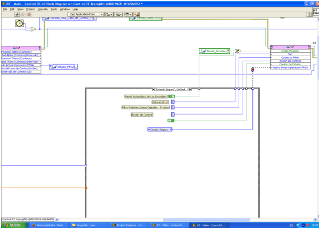
sbRIO-9631 digital inputs/outputs using e/s node FPGAS and FPGA of i/o method node
Hello, I'm trying to configure my SBRio-9631 for the first time. I try to use the on boards to inputs and digital outputs. The following code will work? This is a simple "read the entries, 'or' some inputs and pass ' exits." I have to add "E/s method nodes FPGA" between my 'FPGA of i/o nodes"to get"modes of State of sorting for the input and output lines? Also, I can't simulate/test it works, by adding 5 VDC at the entrances, and not have any source of voltage output. Thank you for your time.
Hey, Spex,.
I really, really appreciate your help. Your follow up information was exceptional.
Thanks again for your help and your time.
gjmm
-
Do not understand why "the node fpga Audio IN Terminal is 16-bit signed integer"?
Hello
I work with myRIO 1900 for my project of ANC.
Audio IN of the fpga node gives its type terminal data as integer signed 16-bit. So, finally the exit on the nodes of the fpga is fluctuating between two values - 1 and 1. But I want the actual values of the audio data, I did not understand how to address this problem.
Audio In on the side of RT gives type of terminal of data such as actual values, but I did not understand why the terminal of Audio In FPGAs is 16-bit integer. ??
Please help me solve this problem.
Thank you.
If your analog range of +/-2.5 V. 32768 then--would be the equivalent of-2.5 V. 32767 would be + 2, 5V.
If you get + /-1 V, then you should see somewhere between + / 13 107 on the analog input of the number I16.
Basically, take the n ° I16, divide by 32767, multiply by 2.5. You will have your analog input in volts.
I don't know why you thing it's just rounding up to the-1 to + 1. Something must be wrong with your code or configuration.
Maybe you are looking for
-
Last location lost or stolen iPad
Hi all I lost my iPad two weeks ago, and no hope, I can't really find I tried to located using "find my iPhone" but the camera has no battery (or the person who 'found' cleared to zero my iPad) My question is: is there a way to access the "history" o
-
Hello, since I've updated for Firefox 27.0.1 on Windows 7, I have a problem with Reporting Services on a Sharepoint site. It is a site of Sharepoint 2010 with SQL Server Reporting Services 2012 Sharepoint integrated mode. I was already on Firefox ver
-
In Mac OS 10.6, why doesn't the shortcut command-n opens a new window of firefox?
Since Firefox 3, n command opens a new window. I'm on a Mac OS 10.6
-
Satellite A100-784: need XP drivers
HelloPlease, can u help me with drivers for A100 XP - 784? All I have is just the video & sound driver... no LAN no wirelles, no bluetooth etc :( I won't use Vista on this machine.Can U give me the links to get the drivers?The model is: PSAANE - 02L0
-
Vista - I'm trying to move a shortcut from my Dropbox one folder my a My Documents folder.
Original title: help I'm trying to move a shortcut from my Dropbox one folder my a My Documents folder. I tells me I need permission to perform this action. I am the administrator then who do I ask? David Ashby