FPGA ni922 24 bit?
I am trying to acquire data from a ni9222 located in the chassis-9014 9114, cRIO.
But for some reason, the output data type is used as a 24-bit fixed point number?
However the 9222 is module of the ADC 4 channels 16-bit 500ks/S.
I want to run the data via a fifo (target scoped) to power a 2 channel FFT module (coregen), which accepts fixed point 16-bit numbers.
I seem to be anyway to change or correct the accuracy.
I increased the fifo to 24 bits to try to work around the problem, but then I can't seem to massage the 16-bit required format (that it should have been originally)
All this in the area of the chassis/FPGA
In another section of my main FPGA vi, I 16 bits of the data of NI9215 quite happily was sent down a DMA FIFO for the time real cRIO and connected to a USB key without any strange problems.
PS are the example any screws available for the use of the FIFO coregen and the 7.1 FFT coregen?
I use the labview 11
In my view, that the data is being multiplied by a scale factor to convert the entry to volts instead of charges. I think it's so when you mix different modules with different resolutions of data acquisition, the outputs are in volts and can be compared, etc.. I know that I changed the properties of some modules for the former counties old-fashioned, but I don't remember exactly how I did it.
Bruce
Tags: NI Software
Similar Questions
-
Do not understand why "the node fpga Audio IN Terminal is 16-bit signed integer"?
Hello
I work with myRIO 1900 for my project of ANC.
Audio IN of the fpga node gives its type terminal data as integer signed 16-bit. So, finally the exit on the nodes of the fpga is fluctuating between two values - 1 and 1. But I want the actual values of the audio data, I did not understand how to address this problem.
Audio In on the side of RT gives type of terminal of data such as actual values, but I did not understand why the terminal of Audio In FPGAs is 16-bit integer. ??
Please help me solve this problem.
Thank you.
If your analog range of +/-2.5 V. 32768 then--would be the equivalent of-2.5 V. 32767 would be + 2, 5V.
If you get + /-1 V, then you should see somewhere between + / 13 107 on the analog input of the number I16.
Basically, take the n ° I16, divide by 32767, multiply by 2.5. You will have your analog input in volts.
I don't know why you thing it's just rounding up to the-1 to + 1. Something must be wrong with your code or configuration.
-
Card FPGA and data acquisition synchronization
Hi, we are control and data acquisition of several hardware devices (including Photodetectors and translational stages). Until last week, we used all the controls and acquisition using a PCIe-7852R FPGA board. However, we decided to move the acquisition part to a PCIe 6363 DAQ card to improve the sharpness of the tension. During the test, I found that the internal clocks in the FPGA and the DAQ cards are slightly inconsistent (not just a phase delay, but a difference in the period).
I know because I have generated a square wave (period = 20) using the FPGA and gains using the data acquisition card (at a rate of 200 kHz, that is, 1 taste every 5). I have observed acquired place shifts 5 every 5 seconds approximately. Such a change does not occur if the production and acquisition is done using the same Board. Therefore, the only explanation is that the data acquisition and FPGA cards clock frequencies are different. According to my calculations, the percentage difference between their time clock must be 5/5 s = 0.0001%.
Therefore, I wonder if there is anyway to synchronize clocks between them. Or, is it possible that I can drive the FPGA clock-based DAQ hardware, or vice versa? Also, please let me know if there is something trivial as I fix.
Thank you very much.
Kind regards
Varun
Hi Varun,
my post was only one solution...
Your data acquisition card may take an entry to control sampling of trigger. In this mode, samples draw on a rising edge of the external clock signal. As long as you stay within the limits of the DAQ (100 MHz for your card) material sampling works perfectly. There are even examples coming with LabVIEW explaining how to program your data acquisition card...
This mode use you your FPGA as clock source sampling for data acquisition. Both will run on the FPGA clock in sync. When the FPGA is a bit out of 40 MHz, so it won't matter because both devices are triggered on the same clock signal...
-
Question for LabVIEW FPGA DRAM
Hi all
How can I correctly address the 128 - bit DRAM memory? I have the Bank DRAM 0 set as a memory of 128 bits, set up in my design as a CLIP. I realize it's a wide RAM on 32-bit. I had a National Instruments AE do the original design I've been adding to. He said that the addresses needed to incrementing by four with each entry. Example: if I had to write in consecutive addresses, I would write to the address: 0, 3, 7, 11, 15 etc, and I would like to send 128 bits to each address. My address is calculated as: (number of pixels in a line of video + line * (number of pixels per line) for a picture of the video). So I take my calculated address and add 4.
However, I checked an example in the finder example: example of integrity hardware flexRIO/IO/external memory/memory. In this example, 128-bit data is sent to the memory and the address is incremented by 1 (instead of 4) each cycle clock as valid data.
Who is this? Section of the help for this function is ambiguous.
Sets the address in external memory for reading or writing. The physical data bus for external memory is 32 bits wide (4 bytes). Each unique address value represents 4 bytes of data. Therefore, the total number of unique addresses in external memory is equal to (Memory Size in bytes)/4.

Note  The memory interface exposed to LabVIEW FPGA is 128 bits wide. As a result, each memory write or read operation accesses four different address locations in memory. The memory controller latches this signal value only when you issue a new memory write command by asserting the Command_Write_Enable signal.
I'm confused by the 2nd paragraph "every Scripture memory or read operation four access address locations of memory." Does that mean I increment the address by 1 to get 128 consecutive bits 'locations' (Yes, I know, that's 4 words of 32 bits in memory), or do I increment the address by 4, in the order of words of 32 bits 4 by 128-bit single transfer?
Thanks for your help.
-J
Hello J,
I want to clarify my previous post. There are two ways to access memory DRAM, CLIP (that you have described is what you do) and using the memory node. As noted before, the DRAM is 128 bits wide. When you write to the CLIP you basically write pieces that is the width of the databus (in this case 32-bit). Therefore, when you write a total of 128-bit DRAM, you place 32 bits in each address. The address being the width of the databus, then you write with a writing & the address 0, 1, 2, 3. Then the next write will be 4, 5, 6, & 7 and then address 8, 9, 10, & 11 and so on. In this case, you must increment your address by 4 whenever you write. Note that you start at 0, then 4, then 8, etc 12. In your previous post, you were out of a figure.
There is also another way to write in the DRAM memory, and it is through the node of memory, which is what is used in the example that you are pointing out. Here, LabVIEW takes on some of the thought, and instead of being the width of the databus address, they are the width of the entire segment of 128 bits. So when you write to DRAM here, you only increment 1 whenever address because they refer to any segment of memory. This contrast with the CLIP, address 0 of the memory node interface match the addresses 0, 1, 2, 3 in CLIP mode & and address 1 of the memory node would correspond to 4, 5, 6, 7 in CLIP mode addresses &. If you do not write an integer of 128 bits for the memory node, then the remaining addresses in the data block are filled with "junk" so that the address remains constant.
As I mentioned previously, it is the most effective writing in chucks of 128 bits so that you don't waste all of the DRAM. I hope you find this explanation clearer.
Brandon Treece
Technical sales engineer
National Instruments
-
How to use a map series R w Teststand?
You put the 'Host' vi in Teststand as said that tests a numerical limit? The host load the FPGA VI in every time his name in TS? The FPGA VI have to compile each time so that the user must wait?
Thank you
You must compile the FPGA in a bit file. You can then load the file bit into the host of VI. This load should only occur when the host VI is executed.
10 minutes to compile? It's fast! I had one that took 2 hours and I've heard stories of some take much longer.
The architecture of producer/consumer is the closest thing that I can compare my configuration. Yes, I use the queues, because the host VI is constantly running. You must use some kind of e-mail in order to pass data in the host VI. I used a driving force to keep my queues in order, but you could probably just use named queues to accomplish the same task.
-
Help! Life or death question :(
Hello guys
IM in the last week of a college project and I need to do some things in labview.
I am receving of a french series FPGA communication. The transmission works OK I will receive the im of data send from the FPGA. With that, my fpga sends 8 bits packets.what I need to to East of put them is a matrix or table is a specific medium.
Sorry if it's not very understandable. Here is a picture of what I'm looking for.
the matrix or table has 4 columns (1 to 4 from right to left) and 16 lines (1 to 16 from top to buttom). the first package of 8-bit should be placed on the column 1-line 1. package, next to colum2-rank 1 and so on. When it gets to 4-row1 colum, the next packet should be placed in row 1 column 2 and so on.
I really hope that someone could give me some suggestions.
Initialize an array of 1 d of 64 items
Each new packect need to replace the element next to the table from 0.
OR
Expand a table with table to build with each new package.
Reshape the picture in 2D.
-
I installed 32-bit and 64-bit LabVIEW 2012 SP1 on Windows 7 X 64 computer. After that, I installed SP1 FPGA Module. While module FPGA completely installed in the 32-bit version and could develop projects fpga, FPGA interface has not installed the 64-bit version. Anyone had this before question?
The document 5WMF8NQ2 knowledge base says it's doable.
I have tried to repair the installed module, remove and then reinstall the module. Nothing helped me to get the FPGA interface on a 64-bit host VI. Any suggestions? Addition of the individual screws through the range of editing functions like a tedious process and the palette is not completely functional.
I solved the problem. Had to repair each driver separately for LabVIEW 2012 SP1 64 bit installed on the default drive. You may need to copy paste files to the folder that it installed in function.
-
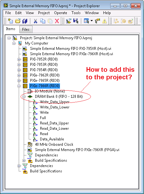
How to add a FIFO 128-bit DRAM to the FPGA project?
How can I add the DRAM FIFO - 128-bit memory Interface to an SMU-796XR RIO module?
Above project is examples of projects. I know how to add DRAM but not how to set as FIFO 128 bits as shown above.
Any guidance is appreciated.
Right-click on the FPGA target-> properties
Select Properties DRAM on the left side of the Popup.
Change the mode of the two shores to CLIP nested LabVIEW FPGA memories.
Click OK.
The project will be auto-updated with new DRAM memory, it will be empty.
Right-click on the DRAM-> properties
Enable
Select FIFO 128 bits
-
64-bit driver for LabVIEW FPGA Xilinx SPARTAN 2009 3rd starting Board
My dear I need this add-on
We I install the module i hava, it seems
Support for LabVIEW for Spartan-3E (incompatible with the 64-bit platform)
is their a supprt 64-bit version?Best regards
Hello mangood,.
There is unfortunately no way to use the driver on 64-bit Windows. You will need to use the 32-bit operating system to use the Spartans drivers. Sorry for the inconvenience.
-
FPGA DDS phase 64-bit register
Hello!
I have some difficulty in updating the code below to use a registry of phase 64-bit instead of just 32-bit or link. I can change the value of control to 64-bit data types, as well as pass the fancy addition with wrap vi to 64-bit. I'm not sure, but how should I change change of logic-5.
Thanks in advance!
http://www.NI.com/example/31066/en/
When you split a U64 you get two U32. The Subvi expected U16 (you see the points of constraint due to incorrect data types).
I suggest shifting the U64 3 bits, then divided in two U32, divide the top once again to the two U16. Since you staggered 3-bit the first 3 bits are 0, resulting in a 13-bit address. The lower U16 is for interpolation.
-
Band bandwidth SMU for FPGA chassis
I'm specing on material for an FPGA FlexRIO system. The module FPGA and adapter, we will use has already been defined, a 7975R and a 5782. For our application, we will be streaming 2 inputs analog on a RT controller attached. From my understanding, these samples will be single precision floating point numbers, each of which is a piece of 4 bytes. Assuming that the 5782 max sampling rate is used, 250 MECH. / s, I think that I will need 2 GB/s of bandwidth on my SMU chassis.
Here my question, then, what SMU chassis should I consider? The SMU-1082 has "up to 2 GB/s per-slot dedicated bandwidth", but it is a real or theoretical number? Normally, I would just get the next thing that high, just to be sure, but there is a significant price difference on the way to the SMU 1085, which is also much larger I need. So I would like to save space and several thousands of dollars if I could get away with a 1082. Sampling does not quite to the max modules of adaptation would be acceptable, but I would be interested to know where about my maximum sampling speed would be.
Thanks in advance for your help.
The 1082 has more than enough bandwidth to stream data at a time to the analog inputs of a 5782. The 5782 has a 14 bit ADC with two channels that sample to 250 ms/s. These samples are returned as an I16 with the two least significant bits filled with zeros.
So assuming that you transfer all I16, rather than packing the 14 bits of data, you would have the following bandwidth requirements.
2 channels x 2 bytes/sample x 250 mega-samples per second = 1 GB/s
The 1082 a 2 GB/s of throughput dedicated per slot. The 7975 accommodates up to 1.6 Gbps streaming. I would recommend calling chat with someone, if you are looking for a recommendation on what type of chassis to purchase, but based on the requirements of streaming that you're fine with the combo 7975 and 1082, you thought. Just make sure you get a controller which can accommodate streaming speeds you're looking for. The 8840 is a good candidate.
-
Digital electronics FPGA Board Hardware Driver for Windows 10
My son just made me aware that his school has a dozen of National Instruments Digital Electronics FPGA boards, but they have never been able to get them to work or actually use them in the curriculum. It seems that he has left his instructor know that I worked with FPGA Xilinx for more than 10 years and now everyone counting on me to get these maps work. The issue seems to be the USB driver. According to the manual, I tried DEFB2012_5_2.exe which simply refused to run on this machine Win 10 x 64. DEFB_4_3.exe ran, but complained that LabView components have not been installed and that it would not continue. Could someone tell me please how to install USB driver ONLY so that we can download files of bits with IMPACT? In terms of a school budget, the investment they have in these maps is not negligible. Thank you.
Hello Dave and TGregor,
I hope I can clear some things here. I'm sorry that you run in so many questions with your boards OF FPGA.
First of all, direct responses:
The LabVIEW FPGA 2015 driver should install the components needed to use the Board with Xilinx tools on WINDOWS 7, it will not work on any system more recent that the pilot has been developed before the release of Windows 8 and 10.
http://www.NI.com/download/NI-Digital-Electronics-FPGA-Board-driver-software-2015/5857/en/
My recommendation for Windows 8 or 10 is rather install Xilinx ISE you find on Xilinx website or on the downloads page OR:
https://www.Xilinx.com/products/design-tools/ISE-design-suite.html
http://www.NI.com/download/LabVIEW-FPGA-Module-2016/6231/en/
The difficulty that you face here is that tool Xilinx ISE is officially supported only on Windows 7 and below. So even though I think it will work (and it will move to the difference in the link of the above driver OF FPGA) for Windows 8 and 10, you can continue to deal with certain issues.
Now you are all looking to program the FPGA using an HDL, Multisim and LabVIEW? If you just use an HDL, you should be all set to go and in the dev environment, you had planned using the program. Circuit design of Multisim 'S simulation tool which includes a complete library of graphic digital components. A digital circuit can be built using the graphical logic gates in Multisim then downloaded directly on the FPGA without first having to learn VHDL or Verilog. It is quite popular among the logical classes digital introduction and we can help you by establishes that as well if you are interested.
For anyone else who might stumble upon this page, I want to make sure you are all aware that, while the Board of Directors OF FPGA is still supported and sold, it has been developed a number of years and has recently been replaced by the Council for development of the digital system (DSDB)that uses a 7020 architecting and has much periphrials more to the program than the FPGA OF. So I know that it is not useful for the current issue, but anyone looking for if they would like to buy more OF FPGA boards, I recommend watching the DSDB instead.
Thank you!
-
With the help of NOR-5641R with FPGA and the instrument driver
Hi Ran,
I don't think what you describe is possible for two reasons.
- You cannot run the pilot bitfile instrument at the same time as a user defined FPGA bit file
- AO ports are AC coupled, so you will not be able to generate a DC bias on them.
-
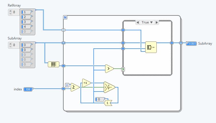
changing/variable index of an array on FPGA
Hi all
I have a question about indexing an array on FPGA. Concretely, I have a constant size 1 M table and want pieces of index of size N of it. Unfortunately, when you try to compile I get the error message: the tables with variable sizes running are not supported. Is there a work-around nice for who?
See you soon
Hello
Well, I don't have first play dynamicaly with the Index of the Array of subset function entry.
This is not supported in a SCTL, so that the planned behavior.
There are several workaround solutions to do this, depending on how you design your design.
1 point by Point approach (as usually made it in FPGAs), using a function table of Index on the RefArray and with the use of counters to keep track of the Index, and evantualy count each sample collected.
This means that every cycle, you have an example that needs to be addressed, you don't work with a tableau more out.
2. same as 1, but using a BRAM I32 element as an interface in the screenshot gave you, I understand that your table with a value of several KBs, which can be a problem in the long term for your design.
3. using a FPGA IP, you could build something like this:
You can use a loop in the context IP FPGA that auto-index the RefArray, to pick up the samples you want, in your sub-table.
This means that you can always work with a table in the output, but the cost will be that you can not leave the subarray in each clock cycle. (use the estimate feature to see the actual flow rate)
4. you can explicitly implement a big MUX, using a box structure. In each case, you provide the desired sub-table.
This is indeed what LV FPGA would do if you where using a standard while loop. Yes, ugly, but no way around it if you want a sub-table, at every clock cycle.
5. the BRAM/DRAM can work with an interface of up to 1024 bits, 32x32bits elements for ex, then you might have used up to 32 items in you case (using the loose I32)
So! In your case, I recommend that you use option 5 if possible:
-Think of BRAMs, your table is starting to get impatient on slices
-Use up to an interface of 1 024 bits on BRAM for a sub-table, do you really need more of 1024 bits a sub-table?
If you don't see how to go from there, I would need more information on what you try to do + all necessary and upstream of the stored data and their data type
Good bye
-
Looking myRIO Xilinx architecting-7010 SoC I am bit inntrested in the workflow for the GS. How does the bennifit myRIO use a system on chip instead of a regulare CPU and FPGA not in the same chip.
4 way could there be to manage a VI?
With FPGA and RT (CPU)
Only of FPGA
Only RT
only the windows
I am comfused, is it any good article/doc describing this?
I found the image in a PowerPoint on the www. -What the task split like this betwheen the CPU and FPGA?
Hello
Please see this link. This can help you understand the architecture of RIO, and there are many whitepapers available in ni.com
Maybe you are looking for
-
The wrongly cloned HARD drive recovery
Hello everyone, Instead of using a third-party cloning software, I tried to clone my drive with disk utility. After restart my laptop, I went into recovery by using the command-R and used disk utility menu in this menu. However, I accidentally chose
-
I have an original Iphone and I try to spend all my photos of her to the Icloud.
I have an original Iphone and I'll try to get all my pictures of it to the Icloud so I can get rid of the phone, but it is not allowing me to do? The phone is Plug and connected to WiFi. But it will move all the photos. Can someone please?
-
Hello Let me first just say, you guys REALLY need phone to do this... like yesterday. In any case, I recently created my online number and he was paid for the year. From my understanding, I was able to receive AND make calls to the United States. Rec
-
The ipad on-air garage band 2 is awesome, finally
I have just download the update on ipad, the new Go is awesome. Finally
-
How can I email photos from my computer? I have a h.p.pavillion and windows vista.
I have windows vista and I downloaded some pictures on my computer. Now, I want to send them a mail and I get a message that it cannot locate my email address. I was told that I have to send via outllook express or msn mail but I was not able to do