FPGA U16
Hello
I have a controller PXI with a PXI-7833R and a PIN of SCB-68 shielded. The entrance of 7833R is - 10 v to 10 v with 16 bit resoluation. Is it possible for me to acquire data from 0V to 10V with the U16 data format? If possible, how to configure the software and hardware.
Thank you very much.
Hello Xiao,
It is not possible to adjust the parameters for the series R ADC. They are set to measure at 09:50, you cannot rotate to measure 0-10 with full resolution. The only options you have change is to say measurement mode, reference signle finished, etc.
So you must either front-end packaging to enjoy more bits, or just the resolution you have.
Hope this helps,
Adam
Tags: NI Hardware
Similar Questions
-
cRIO-9082 DMA bandwidth between RT and FPGA
Hello
I would like to know the bandwidth the cRIO-9082 between FPGA and RT DMA? How many MB/s? I can't find the answer on the web page of NOR.
I know that there are 3 DMA channels, but how fast I could send data from FPGA to memory RT?
What is the optimum size of the element in the DMA channel? U8, U16, U32, or U64?
Material: cRIO-9082 RT
Software: LabVIEW 2012, 2012 LabVIEW FPGA
Best regards
Peter
CLA
-
MODBUS U16 to simple, back from setting in the form
Hello everyone, I am working with a couple inverters Kollmorgen that give and receive data via MODBUS. Using the LabView user's library, I had no problem in the reading and writing of data on their part (assuming I do not more often than 10 times per second). However, I am having some problems with the data format. Kollmorgen has not settled exactly according to the standard and therefore some values are 32-bit registers, some are 64-bit and to initiate, some are signed and some are not; they are all however, delivered in 16-bit of size segments by the function 'read record keeping. Right now I'm only interested in the 32-bit signed value variety.
While I am able to read and I am sure I read the values I want (I can change the value of Kollmorgen workbench and LabView reflects the change of value), the output does not much sense. For positive values, it is fairly intuitive, like the first U16 (I read an array of 2 values U16) is always a zero, and the other is a x 1000 of what positive real value is. So if I read for example a current 3.5 amps, the first U16 is a zero, and the second is 3500; If I read 1.23 amperes is zero and 1230, and so on.
However, when reading negative values, I failed to see a pattern, so that it almost always go to a pretty high value (65 324 or something) in the two registers in low as - number 2. I already tried several data manipulation of the methods listed here, including:
-Conversion of type one in 2 U16 table, then return via join numbers
-Convert the number in binary, binary table then back to number
-Force in single, then using convert in I32 and divide those
So far, no luck, anyone had a similar experience or has worked with these players in the past? Also can't find much information on the documentation of Kollmorgen and their website States that the MSB is sent as the first registry on 64-bit size records. No doubt the positive data format gives a clue, but so far no chance on guessing it.
Convert an I32 U16 table. Divide by 1000.
In the opposite direction. Take your floating point number. Multiply by 1000. Constrain to a U32. Convert to an array of U16.

EDIT: Don't mess with the fixed Point. This is for very special cases, usually involving the FPGA.
-
LabVIEW FPGA: Problem compiling look-up Table
Current versions of software:
LabVIEW 2014 SP1
LabVIEW FPGA 2014
Xilinx Vivado
I'm having a huge problem in trying to compile my LabVIEW FPGA code.
Some recall of the code:
It's all in a SCTL.
I am streaming in a FIFO DMA and comparing it with the values previously stored in the shift registers (which are initialized to 0 at the start of the loop) in the SCTL.
The results of the comparison are then piled into a U16 and loaded into a lookup table (I use the LUT - 1 d), and I'm so help this LUT to decide what value will be charged to travel to record for the next iteration of the loop, which, in any case, would be either the current values of the flow, or the post previous registry value.
(It's a triage loop)
I am able to run very well in simulation mode code, but when I try to compile, I get this error:
"The selected object has a built-in shift register that makes the output on a particular loop iteration correspond to the entries in the previous iteration."
Connect the outputs of the object directly to a minimum number of nodes of Feedback or uninitialized shift registers. You cannot connect the outputs to another object.
See using LabVIEW for more information on the objects with registers embedded offset. »
Someone at - it ideas why this happens, and what might be the possible solutions?
I'm tempted to break it down into separate loops, but I prefer not to because it is now a loop (and working in my simulation).
I found my problem.
Any time that a LUT is in a chain shift register, it cannot:
1. be part of a string of shift register that has a variable initialized
2. follow-up to no decisive structure, like a box structure.
I just moved the position of LUT and it works.
-
Read 1 k samples of 2 bytes each FPGA by UART
Hello
I'm designing a system composed of a board FPGA based (NEXYS4 DDR) which read high speed ADC via the parallel interface. Now, I programmed the FPGA for 1000 samples and send it to a LabVIEW GUI questioned by GUI via UART. Each content sample data 2 bytes so the finals will be 2000 bytes on UART.
At the moment I have not a syntax of separation between samples (to each 2 bytes), do I need? Then when I hit the LabVIEW acquisition he will show me the samples without separation between them.
How is the best way of? To make a separation in the FPGA firmware to each transmission of the sample, or to work with data in LabVIEW and do a syntax with a stacked sequence which will allow me to read 2 bytes and increment an index that will allow me to go to the next 2 bytes.I hope that I was clear where I have my doubts.
In this message, you will find a screenshot that show you how the data looks like when I receive the FPGA. In this screen printing indicator are defined to display the codes and hex display display and 028F is the value of the sample.Thank you in advance,
Vlad
Looks like you are doing things correctly. Just use Unflatten string to convert to a table of U16. I recommend using the Unflatten of string so that you can choose the endianness if necessary.

-
The most effective way to the U16-> U32 Array pack for DMA data transfer?
I have a RT controller who wants to send data to an FPGA using DMA. In LabVIEW 8.2, I have no choice but to switch to the low blocks of data however U32 my my input data is an array of U16. This leaves me two choices: 1) wire U16 table directly into the DMA node that will be rude to U32 but I lose 16 bit * #of table 2) Pack the U16 elements in a U32 table before sending it to the bottom. I have #2 and I have a method that works (and seems to be quite effective) but I have the feeling that I'm doing the hard (or roundabout way). Is their a simpler (but equally effective) way to do this procedure? Thank you
Here's a solution that swaps the bytes and key elements the same. There are several ways to do so.

(for efficiency, you can place the table 'remodel' inside a case structure then, it happens only if necessary)
-
Possible to use the main clock FPGA as a basic Source of time for the NI 9234?
Hello
I am running a NI 9234, and NI 9222 module on a cRIO-9114 chassis with a real-time 9022 controller, data acquisition on the 8 channels on the full sample rate, using the FPGA.
My problem is the synchronization of the data, where the NI9234 is usually a late acquisition, compared to the NI9222. I tried manually delay the NI9222 to take the first samples, but so far without success.
To solve this problem and also to ensure a rate of data more comparable on both cards, I was wondering is it possible to create a Source of time Base master for the NI9234 WITH THE FPGA (opposite to import from another NI9234 or similar module)? The NI9222 I already provide with sampling of the impulses from the FPGA (as expected with this module).
Another issue would be the characteristics of the exact chronology of the two modules, including in terms of synchronization between the beginning of the acquisition and the first samples of data. I couldn't find any information about it...
Thank you in advance,
O Hoppe
Hello!
I've never heard of a possibility to use a time base FPGA with a module of Delta-Sigma.
But I think that the question should be what has not worked to delay the signal and how you did it. Have you read this article?
How can I compensate for delays of different group with the C Series Modules in LabVIEW FPGA?
http://digital.NI.com/public.nsf/allkb/74EB238E1BCADD528625735300681A7DCan you give a more detailed description of your trial to delay acquisitions? Can you provide a code example?
Best regards
Christoph
-
LabVIEW FPGA SPI accident - SPI OR IP address for example - R series OR
Hello
I am trying to run the series R - sample project NI SPI FPGA Simulation.lvproj that comes with the SPI IP OR on a real FlexRIO FPGA SMU-7976R target with an attached digital adaptation NI 6581 B Module. The example is for a PCIe-7841R but I wore during my target FPGA, follow these steps and made additional changes to try to make it work with my set-up. I learned that FlexRIO FAMs CLIPs do not work with nodes in office had so I know I can't simulate the project originally planned so I will try to use FPGA to e/s node host side (open FPGA vi reference) to implement the actual hardware.
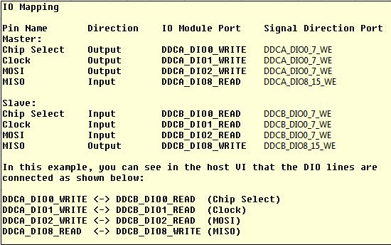
My first question concerns my configuration of the adapter module e/s and selection. I added the IO Module (NI 6581 B: NI 6581 B channel) for my project and selected the channels as shown in the table below. I have a real physical hardware connection as described below using two NI SHC68-C68-D4 cables and a break-out Board.
I changed the names as well:
I selected these DIO channels because I wanted the DDCA connector to be the master and the DDCB connector to be the slave. In addition, in this CLIP every eight channels of i/o has a write enable signal. I have not used the Port configuration because I needed 4 available DIO channels and I saw DIO0-3. Is my logic of selection of channel vs correct Port here?
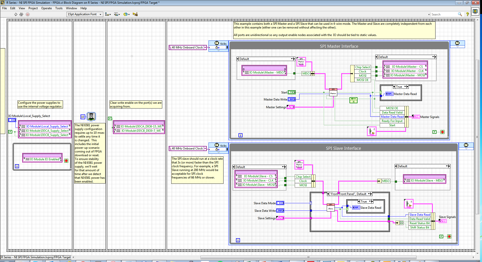
Following the same strategy that examples FlexRIO/NI6581B, I changed the FPGA.vi to include initialization outside of timed loops:
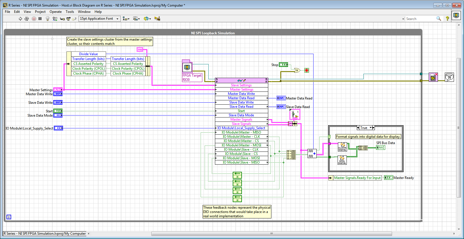
And in the Host.vi I have a node reference FPGA and wired loops of feedback accordingly:
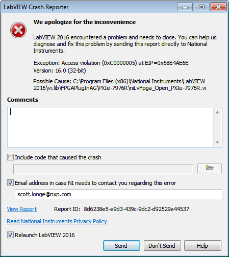
When I compile the FPGA and try to run Host.vi LabVIEW inevitably crashes with Crash Reporter below and must restart:
Does anyone know what I'm doing wrong here? My guess is that it has something to do with the CLIP/IOModule. Any help is appreciated.
Thank you
Scott
Hi Scott,.
I suspect that the problem might be related to the fact that your node open FPGA VI reference is in the while loop and trying to open a new FPGA reference at each iteration.
If you move outside of the while loop, it does not solve the crash?On channel vs port question, your logic seems reasonable to me, but I recommend to try it since this feature could depend on device.
-
I'm looking at the SMU 7857R. I would use the 8 analog inputs and the FPGA to do some annalysisy and DIO based on the best data. I was wondering if it is possible to also define a DAQ task so that all analog data will be made available to the host. Using a data acquisition task would be easier for me to have to write code fpga for use a DMA fifo to send back data.
Hi bcat!
A data acquisition task is only for devices Data Acquisition product supported by driver DAQmx as X-, M-, S-, maps E-Series. The boards of the R series are only supported by the driver OR RIO.
If you don't need pre-treatment on the FPGA so that you can distribute simple data through DMA on your host. If you are looking for an API for the comparable FPGA with the DAQmx API then please check the NI CompactRIO waveform reference library. You can also use the library for R Series boards. -
FPGA/FPGA adapter creates 250 mV voltage offset
I use a high-7971R FPGA in a chassis SMU-1073 with the adaptation Module 5782 (DC coupling) and 2016,08 device drivers. When I turn on the chassis and my computer, nothing strange happens. When I try to run something on the FPGA, however, things get weird. Each piece of code works exactly as it should, but as soon as that 'open FPGA reference' finishes running the adapter begins to produce a voltage mV to 0 to + 250 Ai and AI 1. It doesn't go to AO 0 or 1 AO. This shift of power disappears temporarily as long as 'Reference FPGA open' or "Close FPGA reference" are running, but the only way to get rid of the tension of offset entirely is to restart the chassis. Can someone explain to me why this is happening and how to fix it? The FPGA code, I am running can handle a small shift, but this shift seems to be to saturate the signal.
To see the shift: branch I HAVE 0 and AI 1 directly in a 1 M complete oscilloscope.
It is planned. CDA on this FAM (and more high-end a/d converters) have a range of sampling which is not centered around zero. The front end of the compenstates of the FAM for this by applying an offset from the signal which would appear to the user that the range of the ADC is centered around zero. What is different between this FAMILY and other instruments, is that it is not an additional circuit preventing that this lag observed a user of height of the output of the analog input.
You see the shift happen to reference open FPGA is because that's when power to the GPA is activated. The shift should not have an effect on reading which provides the analog input. Just make sure you have impedance corresponding to the source of the signal at the analogue input and you should be good.
-
Band bandwidth SMU for FPGA chassis
I'm specing on material for an FPGA FlexRIO system. The module FPGA and adapter, we will use has already been defined, a 7975R and a 5782. For our application, we will be streaming 2 inputs analog on a RT controller attached. From my understanding, these samples will be single precision floating point numbers, each of which is a piece of 4 bytes. Assuming that the 5782 max sampling rate is used, 250 MECH. / s, I think that I will need 2 GB/s of bandwidth on my SMU chassis.
Here my question, then, what SMU chassis should I consider? The SMU-1082 has "up to 2 GB/s per-slot dedicated bandwidth", but it is a real or theoretical number? Normally, I would just get the next thing that high, just to be sure, but there is a significant price difference on the way to the SMU 1085, which is also much larger I need. So I would like to save space and several thousands of dollars if I could get away with a 1082. Sampling does not quite to the max modules of adaptation would be acceptable, but I would be interested to know where about my maximum sampling speed would be.
Thanks in advance for your help.
The 1082 has more than enough bandwidth to stream data at a time to the analog inputs of a 5782. The 5782 has a 14 bit ADC with two channels that sample to 250 ms/s. These samples are returned as an I16 with the two least significant bits filled with zeros.
So assuming that you transfer all I16, rather than packing the 14 bits of data, you would have the following bandwidth requirements.
2 channels x 2 bytes/sample x 250 mega-samples per second = 1 GB/s
The 1082 a 2 GB/s of throughput dedicated per slot. The 7975 accommodates up to 1.6 Gbps streaming. I would recommend calling chat with someone, if you are looking for a recommendation on what type of chassis to purchase, but based on the requirements of streaming that you're fine with the combo 7975 and 1082, you thought. Just make sure you get a controller which can accommodate streaming speeds you're looking for. The 8840 is a good candidate.
-
Hello
I would like to smooth out motion of my linear motor. For example, I would like to start a program on the cRIO in scan mode Let's say 1ms interval scan and then perform the interpolation between the points of output (for example, the wave of fishing) on the scan interval 100us. FPGA I wrote programs little but my linear motor does not move. I can't find where I made a mistake or / and something is missing.
Any help would be approciated.
I put in the attachment of my FPGA file, but also the host file I have on the cRIO.
Thank you.
Kamil
Dear Alex,
Thank you interested in my topic. I just understood how do. I went by this example: http://www.ni.com/product-documentation/3598/en/. However I have modyfied somewhat FPGA interpolation method. One described is nove myself smooth enough movement. I have attached files if anyone will need one day. I think that the case is closed.
-
Hello
I use card FPGA 7966R with Module of e/s 6587. I have two sets of screws FPGA, one that uses 6587 mode series (Serdi channel) and the other in parallel mode (Serdi connector). I'm trying to select one of the FPGA VIs via the host VI and I don't know if it's possible.
Some things to note:
- All IOs have the same names, FIFO has the same data type and name.
- Because they use the IO 6587 controller in a different configuration, I can't parallelize them and combine them into a single VI.
Thank you
MILIN
You should take a look at the function of Bitfile dynamic reference opened .
-
Control of read/write of FPGA Interface
I need help on control of FPGA read/write Interface. I would like to connect data TCP Read (String) directly to VI FPGA Read, but the entrance is an FXP... How can I do this?
Then change your FPGA control to be a byte (U8). On the side of your host, use the array of strings of bytes, then Index Array to get the specific byte you want to write on the FPGA.
-
Digital electronics FPGA Board Hardware Driver for Windows 10
My son just made me aware that his school has a dozen of National Instruments Digital Electronics FPGA boards, but they have never been able to get them to work or actually use them in the curriculum. It seems that he has left his instructor know that I worked with FPGA Xilinx for more than 10 years and now everyone counting on me to get these maps work. The issue seems to be the USB driver. According to the manual, I tried DEFB2012_5_2.exe which simply refused to run on this machine Win 10 x 64. DEFB_4_3.exe ran, but complained that LabView components have not been installed and that it would not continue. Could someone tell me please how to install USB driver ONLY so that we can download files of bits with IMPACT? In terms of a school budget, the investment they have in these maps is not negligible. Thank you.
Hello Dave and TGregor,
I hope I can clear some things here. I'm sorry that you run in so many questions with your boards OF FPGA.
First of all, direct responses:
The LabVIEW FPGA 2015 driver should install the components needed to use the Board with Xilinx tools on WINDOWS 7, it will not work on any system more recent that the pilot has been developed before the release of Windows 8 and 10.
http://www.NI.com/download/NI-Digital-Electronics-FPGA-Board-driver-software-2015/5857/en/
My recommendation for Windows 8 or 10 is rather install Xilinx ISE you find on Xilinx website or on the downloads page OR:
https://www.Xilinx.com/products/design-tools/ISE-design-suite.html
http://www.NI.com/download/LabVIEW-FPGA-Module-2016/6231/en/
The difficulty that you face here is that tool Xilinx ISE is officially supported only on Windows 7 and below. So even though I think it will work (and it will move to the difference in the link of the above driver OF FPGA) for Windows 8 and 10, you can continue to deal with certain issues.
Now you are all looking to program the FPGA using an HDL, Multisim and LabVIEW? If you just use an HDL, you should be all set to go and in the dev environment, you had planned using the program. Circuit design of Multisim 'S simulation tool which includes a complete library of graphic digital components. A digital circuit can be built using the graphical logic gates in Multisim then downloaded directly on the FPGA without first having to learn VHDL or Verilog. It is quite popular among the logical classes digital introduction and we can help you by establishes that as well if you are interested.
For anyone else who might stumble upon this page, I want to make sure you are all aware that, while the Board of Directors OF FPGA is still supported and sold, it has been developed a number of years and has recently been replaced by the Council for development of the digital system (DSDB)that uses a 7020 architecting and has much periphrials more to the program than the FPGA OF. So I know that it is not useful for the current issue, but anyone looking for if they would like to buy more OF FPGA boards, I recommend watching the DSDB instead.
Thank you!

Maybe you are looking for
-
Broken hard drive and no Windows 8 sticker
Hello I have a Toshiba laptop, * the HDD is broken * and when I bought did not have recovery disk. Nobody told me that I had to make a copy on the disc when the phone still worked. Now I have a new hard drive but does not have the recovery partition
-
ProBook 450 G2: SD ard drive does not
Hi there, it anyone have a driver for ProBook 450 G2 for card reader. 8.1 to win. 64 bit Have installed all the drivers page from HP, all the works of material however, support SD card driver does not work. Thank you
-
macBook Pro 10.5.8 does not update Safari Firefox Google. Why? What should do?
macBook Pro 10.5.8 does not update Safari Firefox Google. Why? What should do?
-
When I try to connect to my Windows 2003 domain controller server, I get the following messdage: The DOMAIN CONTROLLER FOR THE DOMAIN (DOMAIN NAME) cannot BE CONTACT. How CAN I SOLVE THIS PROBLEM?
-
Intermittent slow internet connection
I've been running windows 7 (64 bit professional) for several months now and at first, everything was great. However in the last few weeks (maybe even as long as 2 months) I've known internet connection problems. All started with my computer randomly