SMU 7857R FPGA and DAQ task
I'm looking at the SMU 7857R. I would use the 8 analog inputs and the FPGA to do some annalysisy and DIO based on the best data. I was wondering if it is possible to also define a DAQ task so that all analog data will be made available to the host. Using a data acquisition task would be easier for me to have to write code fpga for use a DMA fifo to send back data.
Hi bcat!
A data acquisition task is only for devices Data Acquisition product supported by driver DAQmx as X-, M-, S-, maps E-Series. The boards of the R series are only supported by the driver OR RIO.
If you don't need pre-treatment on the FPGA so that you can distribute simple data through DMA on your host. If you are looking for an API for the comparable FPGA with the DAQmx API then please check the NI CompactRIO waveform reference library. You can also use the library for R Series boards.
Tags: NI Hardware
Similar Questions
-
Looking myRIO Xilinx architecting-7010 SoC I am bit inntrested in the workflow for the GS. How does the bennifit myRIO use a system on chip instead of a regulare CPU and FPGA not in the same chip.
4 way could there be to manage a VI?
With FPGA and RT (CPU)
Only of FPGA
Only RT
only the windows
I am comfused, is it any good article/doc describing this?
I found the image in a PowerPoint on the www. -What the task split like this betwheen the CPU and FPGA?
Hello
Please see this link. This can help you understand the architecture of RIO, and there are many whitepapers available in ni.com
-
NOR-5781 Baseband Transceiver and OR SMU-7962R (FPGA)
I'm looking for an example of code to transmit videos using OFDM in LabVIEW between two different units of the PXI. I have two different sets of NOR-5781 Baseband Transceiver and NI SMU-7962R (FPGA) installed in two PXIs. One is the sole issuer and another is to be alone receiver.
Are there examples of code to trasnmit video with the help of these above mentioned devices preferably via OFDM in LabVIEW.
Thanks in advance.
Hey Joseph,.
If you look at the 5781 start-up project, you will see that the analog input and output of the sections of the code are separated. You will want to remove the section of code of analog output of the side Rx and remove the analog input on the side of Tx section. At this point, you would have a functional code that would send signals to a chassis to another, you simply add this necessary to the wave before you write it on the device of modulation and demodulation subsequently shape wave after receipt.
The examples are intended to be a starting point, and I think that you can access your ultimate goal without much change (remove unnecessary parts of the code and the addition of modulation).
-
Band bandwidth SMU for FPGA chassis
I'm specing on material for an FPGA FlexRIO system. The module FPGA and adapter, we will use has already been defined, a 7975R and a 5782. For our application, we will be streaming 2 inputs analog on a RT controller attached. From my understanding, these samples will be single precision floating point numbers, each of which is a piece of 4 bytes. Assuming that the 5782 max sampling rate is used, 250 MECH. / s, I think that I will need 2 GB/s of bandwidth on my SMU chassis.
Here my question, then, what SMU chassis should I consider? The SMU-1082 has "up to 2 GB/s per-slot dedicated bandwidth", but it is a real or theoretical number? Normally, I would just get the next thing that high, just to be sure, but there is a significant price difference on the way to the SMU 1085, which is also much larger I need. So I would like to save space and several thousands of dollars if I could get away with a 1082. Sampling does not quite to the max modules of adaptation would be acceptable, but I would be interested to know where about my maximum sampling speed would be.
Thanks in advance for your help.
The 1082 has more than enough bandwidth to stream data at a time to the analog inputs of a 5782. The 5782 has a 14 bit ADC with two channels that sample to 250 ms/s. These samples are returned as an I16 with the two least significant bits filled with zeros.
So assuming that you transfer all I16, rather than packing the 14 bits of data, you would have the following bandwidth requirements.
2 channels x 2 bytes/sample x 250 mega-samples per second = 1 GB/s
The 1082 a 2 GB/s of throughput dedicated per slot. The 7975 accommodates up to 1.6 Gbps streaming. I would recommend calling chat with someone, if you are looking for a recommendation on what type of chassis to purchase, but based on the requirements of streaming that you're fine with the combo 7975 and 1082, you thought. Just make sure you get a controller which can accommodate streaming speeds you're looking for. The 8840 is a good candidate.
-
Synchronize PXI-8512/2 and DAQ, PXI-6220 CAN
Hello
I read some examples and other posts on the topic "sync", but I need more information.
I'm using a PXI-8512/2 with an older application, based on the API of frame. Several frames are transmitted and received periodically, and I need to enter a unique ID of arbitration which has a cycle of ~ 5 ms.
At the same time, I need a task of data acquisition (analog input) with a sampling frequency of 1000 Hz.
The challenge is, I need to have the same time base for the analog input and CAN.
As far as I understand, the timestamps CAN are created in the PXI-8512. The timestamp of the start of the DAQ tasks is based on the time of OS (Windows).
Transmission/reception CAN must be running still (to perpetuate the ECU), and the data acquisition task will be triggered manually.
I found the example '\nican\Frame - base with NI - DAQmx.llb\CAN Frame entry API DAQmx Input.vi'. It fits my needs? There is a comment saying: "the departure of AI uses the same sampling as CAN. What it means? The sampling frequency of my CAN is fundamentally different from DAQ. But I have to be able to associate each sample DAQ for a CAN of armature (same time base).
Thank you for any information helping to clarify.
Concerning
Hello
Sorry, I don't know why I thought you had an X-Series. There is also an example for the other series with the XNET driver:
Synchronize PXI - CAN with analog DAQmx of entry (using the PXI-Clk10) .vi
Kind regards
Heinz
-
Card FPGA and data acquisition synchronization
Hi, we are control and data acquisition of several hardware devices (including Photodetectors and translational stages). Until last week, we used all the controls and acquisition using a PCIe-7852R FPGA board. However, we decided to move the acquisition part to a PCIe 6363 DAQ card to improve the sharpness of the tension. During the test, I found that the internal clocks in the FPGA and the DAQ cards are slightly inconsistent (not just a phase delay, but a difference in the period).
I know because I have generated a square wave (period = 20) using the FPGA and gains using the data acquisition card (at a rate of 200 kHz, that is, 1 taste every 5). I have observed acquired place shifts 5 every 5 seconds approximately. Such a change does not occur if the production and acquisition is done using the same Board. Therefore, the only explanation is that the data acquisition and FPGA cards clock frequencies are different. According to my calculations, the percentage difference between their time clock must be 5/5 s = 0.0001%.
Therefore, I wonder if there is anyway to synchronize clocks between them. Or, is it possible that I can drive the FPGA clock-based DAQ hardware, or vice versa? Also, please let me know if there is something trivial as I fix.
Thank you very much.
Kind regards
Varun
Hi Varun,
my post was only one solution...
Your data acquisition card may take an entry to control sampling of trigger. In this mode, samples draw on a rising edge of the external clock signal. As long as you stay within the limits of the DAQ (100 MHz for your card) material sampling works perfectly. There are even examples coming with LabVIEW explaining how to program your data acquisition card...
This mode use you your FPGA as clock source sampling for data acquisition. Both will run on the FPGA clock in sync. When the FPGA is a bit out of 40 MHz, so it won't matter because both devices are triggered on the same clock signal...
-
I found a few larger images (986 x 1024 and 2420 x 2514) I'd like to see on the entire screen. Is there a way to do this by enabling / disabling (then restore it later) of all toolbars - including the status bar and the task bar? Or is there an FF extension that will make perhaps even easier?
Press F11 or select "full screen" in the menu. (If there is still floating toolbars around after that, do a right-click on the toolbar and remove the checkbox.)
-
Hi all
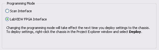
We have NI 9421 digital input and digital output NI 9472 Modules. We can run these modules into a VI under the 9073 cRIO chassis. While we have added the FPGA target under the same chassis, we cannot use the modules. We also install the scan engine.
How can we use FPGAS and i/o Modules at the same time?
Once you add a target FPGA in CompactRIO chassis, when you deploy the code, the cRIO is configured for the FPGA mode, which requires a bitfile compiled to connect with the C Series modules. Remove the target FPGA or changing the mode of chassis in the project and by redeploying must reconfigure the cRIO for scan Mode, which allows you to use the IO module directly from the RT VI.
For more information, see this post.
-
Where can I find list of pins for connectors 68 pins on the SMU-8430/8 and the SMU-8431/8
We need to build new cables for the SMU-8430/8 and 8431/8 interface cards series.
I can't find pinout information or other connectors 68-pin on the front of these cards.
Can someone point me in the right direction to find this information. Thank you.
The design of the system requires new cables we don't need a list of the pins.
After a few more watching on the web site of NOR, I found the information I need here:
http://digital.NI.com/manuals.nsf/WebSearch/F5A76AD1B0C3B1FE86257B59006A9EAD
Thanks for the reply.
-
What is the use of FPGAS and how it differs from the IO Modules
Hi all
Maybe it's a silly question for most of you. But I have very less knowledge about the basic concepts of electronic (FPGA, real-time) to cRIOs. I know that FPGA
can be used to generate circuits within the chip that helps by some logical functions.
I've just started working in the cRIO. My question is that we have Modules e/s making it outputs all the application entry. So, what is the purpose of e/s in the FPGA.
Lets consider that we entered for an application of RTD. In this case the module NI 9217 itself exits 24 bits of data from the RTD measurement which may be the process of the LabVIEW VI. What will be this FPGA between the i/o Modules and the processor will help in? Also I want to know what type of communication is used to send data between the FPGA and host modules.
Thanks in advance
Ajay HI:
Sorry, you do not have an answer to your original question. However, you are right about the benefits of the FPGA. You said, if you build pre-processing in the FPGA, you can unload a lot of potentially CPU calculations out of the host processor. In addition, the program running on the FPGA is highly deterministic and can run the code very quickly. So if you build a kind of guard or evanescent dog part of your application, the FPGA is a good place to put it.
To answer your other questions, communication between the modules and the FPGA is generally above the SPI and the data can be transferred between the FPGA and host via DMA FIFO operating on the PCI bus or single point save access using read/write in the FPGA host Interface controls. You can also use interruptions in signal of disputes between the FPGA host.
I hope this helps, but let us know if you have any other questions.
-
Number of DMA FIFO of items to read mismatch in the FPGA and RT
Hi all
I use myRIO, LV14 to run my application.
Request: I have to continuously acquire data via FPGA and host RT process once every 2000 samples are taken. I use DMA FIFO (size 8191) to acquire data, use timeout property in the FPGA to eliminate the buffer overflow. I had followed cRIOdevguide to implement this part. An excerpt of what I put in place is attached. All code runs in the SCTL at 50 MHz.
Question: Two or three times I met with this strange behavior, the FPGA FIFO gives continous timeout and the RT is unable to read the FIFO. The number of elements to set the property in the FPGA VI gives 0 showing that FIFO is full and no more can be written, but the RT, remaining items gives 0, so it is reading 0 (none) elements.
Solution: I put a case where I'll write to FIFO (under the code) and if the number of elements to write is different from zero. It seems to work fine, from now.
What confuses me, is that my FPGA VI said that FIFO is full (number of items to write 0 = FIFO) and gives a timeout error, but RT VI said that number of items remaining in the FIFO is 0 and therefore no data is read. No idea why this is so? My RT and FPGA VIs continues to run, but with no gains or to read data.
A few minutes after you run the code, I've seen this behavior. No idea why this happens? I try to reproduce the behavior, and will update if I meet with her again. Sorry, I can't post my code here, but I guess the code snippets to explain some extend.
Thank you
Arya
Edit: Even with the mentioned workaround solution, the problem persists, now that the FPGA written any of FIFO. And the RT VI is not able to read all the elements he sees 0 items in the FIFO. The FIFO continues to be in a State of timeout. So I guess that the problem is on the side of RT.
Why it looks like you read from the FIFO even in two different places in the same VI, at the same time? If the lower reading throws the FIFO, it will never trigger the reset, which could lead to the situation you describe, I think (it's hard to tell from a few screenshots).
Also, your logic seems too complicated. I immediately noticed that there is no reason to select the entry, the output of = 0 - simply use the 'equal to zero' output directly. On the side of FPGA, why you need check the number of items that you want to write? There's nothing wrong with writing in a FIFO that is already full. just the data won't get written.
-
How to use the target FPGA and co. on the same chassis cRIO?
I have a cRIO system consisting of a master chassis 9074 with several modules IO and EtherCAT 9144 slave unit.
I want to run a CIE (see: http://zone.ni.com/devzone/cda/epd/p/id/5333) on the chassis of the master, this uses the analytical engine. At the same time I have to do some very urgent measures if I want to use the Board in hybrid mode, using analysis and FPGA engine at the same time (as described here: http://digital.ni.com/public.nsf/allkb/0DB7FEF37C26AF85862575C400531690.)
But as soon as I add the FPGA target at one of the chassis, the feature of the ice on this chassis stops working. After some research, I found that the CIE can initialize is no longer the modules belonging to the frame that has the target FPGA on it. Error in the method Init of the CIE is: 65700 (indeterminate). This occurs when you try to use "for a more specific class' on the modules configured with a target FPGA on it.
Someone knows what can cause exactly this problem and perhaps provide a solution/work around?
Many thanks in advance.
Hybrid mode requires you to have a bitfile compiled running on the FPGA to be able to read the Scan Interface IO Variables. Move the target FPGA at the RT target module will allow Interface of scanning for this module, but the frame will always mode Interface of LabVIEW FPGA.
To get fair access to the scan mode for the frame, right click on the chassis in the project, and choose Properties. Then, modify the Scan Interface programming. If you want to continue using the programming of FPGA and the Scan Interface set (hybrid mode), you will need to compile a bitfile (empty if you do not want programs on the FPGA again or containing your FPGA code). By compiling, the support of the module scan mode for the modules under your RT chassis is compiled in your custom bitfile. Then, on your VI RT, you need to use reference FPGA VI open to your newly compiled VI. Once this VI is deployed and ongoing implementation, you get the data from you are the CIE.
For more information, see this knowledge base article and Reference Interface of Scan CompactRIO and procedures.
-
LabVIEW FPGA and real-time communication module
Hi all
I created a small program in labview FPGA which gets continually distance from the HC - SR04 ultrasonic sensor. The rest of the robot program is written in the time module real Labview. Is it possible that the distance calculated by FPGA module to read in time real module.
I used the FPGA just because there micro-deuxieme counter, which helps me get the distance from the ultrasonic sensor.
Thanks in advance.
There are many ways this can be done, according to your needs.
See the help article transfer of data between the FPGA and host (Module FPGA) for a breakdown of each method.
-
What are the differences between LabVIEW and LabVIEW FPGA and LabVIEW RT
I need a comparison of LabVIEW, LabVIEW FPGA, and LabVIEW RT
Sorry, I misunderstood.
LabVIEW RT (LabVIEW Real-time) combines graphical LabVIEW of programming with the power of a real-time operating system, allowing you to create applications in real time.
-
While the closure of the pc I got the message: "1 program still needs to be closed: (pending of) task host window's task to stop execution and stop tasks that are already running".but there is no program running and I have to force it to close.how to solve?
Hello
Thank you for contacting Microsoft Community.Windows, then closing, checks all open programs. If there is, it sends a request for the program to close and wait until the program closes safely, to avoid any loss of data. But, Windows is waiting for some specifiedIf you are sure that none of the programs are obviously open, you can try the following steps:Press Windows key + r, Type regedit and pres enter. If UAC prompts, click Yes. Go to HKEY_LOCAL_MACHINE-> expand System-> expand CurrentControlSet-> click on command (exapnd no do this). When you click (or select) control, you can see WaitToKillServiceTimeout. Double-click it to change the value. Set the value to 500 or less than that. Click Ok, and then close the registry editor. Now, restart the PC. If the problem persists, stop and try again and check.Be careful with registry access as incorrect values or remove the unknown keys can prevent Windows to start and it will fix it.Response if the issue is not resolved.
Maybe you are looking for
-
just installed Firefox V8; It is supposed to be a bookmarks button, but I did not!
I have the front/back arrows, area URL, a search box Google, the Adblock plus button and the home button. And nothing more... Where is the favorite button announced? Or how can I create it myself?
-
Good evening everyone, I recently had my 8.1 Windows reinstalled on my laptop through a 3rd party shop. As you know they wipe everything what there including programs initially on the laptop to buy. I wasn't ready to pay the price, they cited for all
-
rtil20.BPL not installed using programs.do block I need to this and what I do?
start a Sunrise I have a CSA Board .exe pop saying I need to install rtil20.bpl which is not on my computer.What is c? what I install and how?Help, please.
-
WndOws 10 on Stream 7 5709 wll not install
Although many people on this site of the Community said that they were able to load Win 10, feel for the mistake that wll Win 10 statng load not because I am usng an OS compressed. Any help would be wonderful - thank you for your time!
-
Windows Update Error 80070020 cannot install updates.
I was not able to install updates 12/06/2012 when the Update window 7.6.7600.256 Agent has been installed. When I try to update I get - install new Windows software update: to check the updates, you must first install an update from Windows Update.