Interpolation on the FPGA
Hello
I would like to smooth out motion of my linear motor. For example, I would like to start a program on the cRIO in scan mode Let's say 1ms interval scan and then perform the interpolation between the points of output (for example, the wave of fishing) on the scan interval 100us. FPGA I wrote programs little but my linear motor does not move. I can't find where I made a mistake or / and something is missing.
Any help would be approciated.
I put in the attachment of my FPGA file, but also the host file I have on the cRIO.
Thank you.
Kamil
Dear Alex,
Thank you interested in my topic. I just understood how do. I went by this example: http://www.ni.com/product-documentation/3598/en/. However I have modyfied somewhat FPGA interpolation method. One described is nove myself smooth enough movement. I have attached files if anyone will need one day. I think that the case is closed.
Tags: NI Hardware
Similar Questions
-
Error-63101 when executing the FPGA Interface C API Generator in LabVIEW 2012
I'm using LabWindows CVI 2012 and 2012 LabVIEW FPGA module. I try to use the FPGA Interface C API generator and I get the following error from a freshly generated .lvbitx bitfile. I use the local server compiles on my PC.
Error-63101
NOR-RIO: A valid .lvbitx bitfile is required. If you are using a valid .lvbitx bitfile, the bitfile maybe isn't compatible with the software you use. Determine which version of LabVIEW was used to make the bitfile, upgrade your software to this version or later, and then try again.
The problem occurs when executing CVI or LabVIEW. I was able to do this earlier when I was compiling the FPGA in LabVIEW with the API generator 2011 downloaded from the Web site.
A bit of weirdness in my setup, it's that I charged it off downloads from the website (latest files after 2012 NIWeek) rather than the normal distribution DVD. I installed LabVIEW, so NI RIO, then the Xilinx tools compatible with 2012. It works very well when you talk to the FPGA to a LabVIEW vi running on my Windows PC to the host.
Any suggestions?
Problem solved. I had to download FPGA Interface C API generator 12.0. It works now.
I would have thought that if a product was called on the menu in LabVIEW 2012, it would be prompted to upgrade to a compatible version, when I installed LabVIEW. The old version is not compatible with version 3.0 bitfiles, as identified on the following lines at the top of the .lvbitx file:
3.0 -
24 v digital signal of the event from the host to the fpga power on/off
Hello forums or
Sheet material
cRIO-9074
module or 9472 digital module 24 V output c series
To expand on the topic described,
I want to be able send a trigger to alarm the fpga digital 9472 out that lasts 30 seconds using the operating system time real clock time on the host computer
The way I approached this problem is that
In the loop where the event occurs, if the event trigger is defined then the fgv has a time stamp when the event occurred is sent.
In the loop that communicates with the control of fpga, I write to the control based on the condition that the difference of the current time checked and fgv time is 30 seconds or less, then it will send the value true, otherwise send fake and wait for the next occurrence of the event.
The main problem after implementation of this is that 9472 led does not turn off when the false value is sent to it.
cordially Mzamanstl
Timer Keeper SD is a FGV so that it is written for her, once the event occurs
So if the event occurs so timestamp is stored and then the difference of the timestamp result is<30>
then a true value will be sent to the module of 9472
So basically I want the light and I want to do the 24 v output for 30 seconds then turn off and wait for the next occurrence
I think the method that I test it with is not very good, because I realize other factors that may contribute to this problem, so I think I found another way to test
and I will try it but its will take time.
cordially Mzamanstl
-
Broken the FPGA VI but the empty error list
Hello!
I'm trying to run a vi which includes a 'Open FPGA VI Référence' function. However, an error and it says that "not compiled FPGA VI. When I try to compile the FPGA VI a message saying "The VI is broken". I try to run the FPGA and when appears in the error list, there is no error or warning in the list, although the name on the fpga includes the Red 'X' ('show warnings' is checked). Any help?
I'm using Labview 2013.
Pablo
Hi Pablo.
Sorry for my delay in responding, you managed to get the respected FPGA.vi yet?
To answer your questions, if the project is ok with an empty FPGA.vi, then in theory, your hardware is configured ok. However, due to the vi being blank, you haven't tried to use one of the modules on your system, so it can introduce errors. The most common mistake is differentiation of mode Scan Mode/FPGA by installing the project in the first place. Also be aware that not all FPGA targets supports everything, for example some dislike for the rows that have an index to calculate the number of iterations, rather than a constant wired at the entrance to "n".
Out of curiosity, why you place every measure in the DMA separately and also specify address? Is there a reason you don't just place all the measures in a table and put everything in the DMA, then divide the table on the other side?
Generally speaking I don't think that incorrect programming should never cause LabVIEW crashing and you should always report the problem to the OR in order to take a look and see if they can fix it.
Hope that you managed to get your problem sorted and again sorry for the late reply.
Darren.
-
Areas of clock in the FPGA examples
I was looking through some examples of LabVIEW FPGA and I fell on the example of Crossing Clock domains.
In this example, there are 4 screws; FIFOs.vi; Global Variables.vi; Local variables.VI; and Registers.vi. In each of these screws, there is a timed loop which runs at 160 MHz.
How is that possible? Since the clock on the FPGA is only 40 MHz. did I miss something?
On the FPGA target, you can right click on the clock of 40 MHz and create a derived clock which can be a multiple where for a fraction of the base clock (40 MHz).
160 MHz is a trivial example of 4 times the base clock.
-
Why get error during execution the FPGA VI?
Hello world
I have a lot of sense of wrong during execution of a program that has been correctly executed previously. I don't know what I did wrong.
Now, whenever I run this FPGA VI, I get an error (in the attachment). And, then runs the FPGA VI, but it does not give the data required those he supposed to give as output.
Any help or recommendations would be appreciated also.
Thank you.
Hi auree123,
There are a few reasons for this error
may occur. Could you tell us more about what's going on?You are
I get this error when you compile and if so, at what stage?It looks like
as you may be running it in Interactive Mode, which means that you are viewing
the front of the FPGA VI on the development computer that you are running - is
that correct? If so, you could try to create a VI on your host
Open a FPGA reference and communicate with the FPGA programmatically rather than interactively.Thank you
Morgan S
Technical sales engineer
-
Can damage the FPGA module if I connect accidentally two pins writing together.
My current configuration has a PXI chassis with two FPGA modules. Each FPGA module has an adaptation Module 6581 on that. I would like to test the signal through my system path by having the user to move some cables that would be a reason for a return to the other looping FPGA.
I fear, however, the risk of the user is not correctly as shown and somehow a channel available in writing that connects to another channel write-enabled. This damage to the FPGA or adaptation modules?
Hi Brian,.
Your concerns are correct. We never want to connect two pins that are output voltage. If two pins are outputs digital mistakenly connecting them together may damage one or both nodes in output since there is nowhere to flow the potential.
It is well to connect to two pins that read a voltage. If both pins running entry digital (reading of the pins), as there is no risk, nor pin would be likely to be damaged.
-
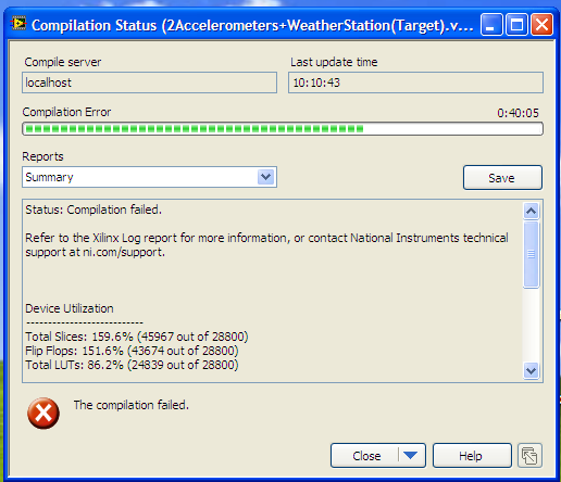
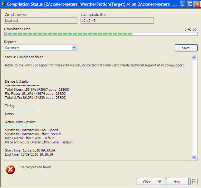
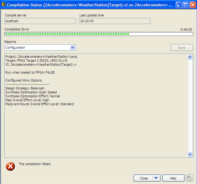
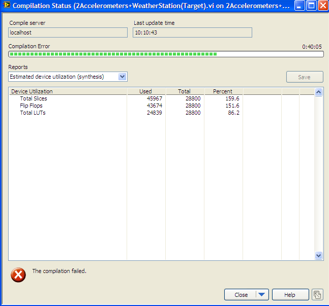
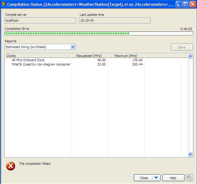
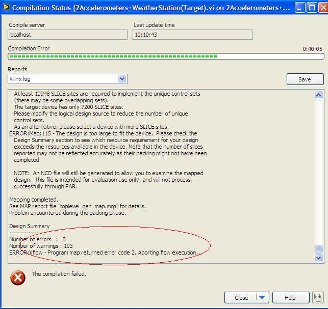
ERROR: TclTasksC:process_077: in the FPGA Compilation
Hi all
I use for my application in which I am facing following error when compiling my fpga code compact rio 9072:
Compilation failed due to an error of Xilinx.
Details:
ERROR: TclTasksC rocess_077: did not finish. Please, look in the newspaper and report files.false
When running
"process run"card.
(file "C:\NIFPGA\jobs\XI64xG6_My449tj\map.tcl" line 6)ERROR
ack:2310 - type compositions "SLICEL" too found to adapt to this device.
ERRORack:18 - the design is too large for the device and package.
Please see the Design summary section to see the cost estimates for
your design exceeds the resources available in the device.
NOTE: A file NCD will be always generated to allow you to examine the mapped
Design. This file is intended for assessment use only and will not be processed
successfully through NOMINAL.
This NCD mapped file can be used to assess how the logic of the design has been
mapped in FPGA logic resources. It can also be used to analyze
preliminary to the level logic (route pre) calendar with one of the static electricity of Xilinx
analysis of synchronization (PRHT or Timing Analyzer) tools.
Summary of the design:
Error number: 2
Number of warnings: 69
Use of logic:
Number of slice Flip Flops: 7 886 on 15 360 51%
Number of 4-input lut: 16 104 on 15 360 104% (OVERMAPPED)
Distribution of logic:
Number of slots occupied: 8 744 7 680 113% (OVERMAPPED)
Number of slices only related logical container: 8 744 100% 8 744
Number of slices that contains no logical relationship: 0 to 8 744 0%
* See NOTES below for an explanation of the effects of unrelated logic.
Total number of 4 input lut: 17 400 on 15 360 113% (OVERMAPPED)
Number used as logic: 15 998
Number used as a middle way: 1 296
Number used as Rams 16 x 1: 82
Used number recorded the shift: 24
The logical Distribution report slice is not significant if the design is
too mapped to a resource not slices or if Placement fails.
Number of IOBs servile: 183 on 333 54%
BIO flip flops: 74
Number of RAMB16s: 1 24 4%
Number of MULT18X18s: 2 on 24 8%
Number of BUFGMUXs: 4 to 8 50%
Number of DCMs: 1 on 4 25%
Fanout of the Non-horloge nets on average: 3.38
Peak Memory use: 361 MB
Total in time REAL in the completion of the card: 1 dry 12 mins
Time CPU until the end of the total map: 1 dry 12 mins
NOTES:
Related logic is defined as logical that share connectivity - for example two
Lut are "related" if they share common inputs. During Assembly of the slices.
Card gives priority to combine the logic that is related. Generates so
best performance of synchronization.
Without logical report does share no connectivity. Card will start only packing
logic not related in a slice once that 99% of the slices are held through
logical packaging partners.
Note that once the logical distribution reaches the level of 99% by related
logical packaging, this does not mean the device is completely used.
No logical report package will begin, continuing until all usable LUTs
and FFs are busy. According to your timing budget, an increase in the concentrations of
logical packaging unrelated can adversely affect the performance of timing set
your design.
Mapping performed.
See the report of map file "toplevel_gen_map.mrp" for more details.
Problem encountered during the packaging phase.
Failure of the process 'Map '.Start time: 18:29:23
End time: 18:44:42
Total time: 00:15:19Can someone tell me why this error came?
Thank you best regards &,.
Vipin Ahuja
Vipin Hello,
It seems that your code requires more resources that are available on the FPGA. Optimizing your code can help to solve your problem:
You may have noticed some "Overmapping", mentioned in the newspaper:
Number of 4-input lut: 16 104 on 15 360 104% (OVERMAPPED)
Distribution of logic:
Number of slots occupied: 8 744 7 680 113% (OVERMAPPED)Take a look at this article:
http://digital.NI.com/public.nsf/allkb/060BA89FE3A0119E48256E850048FFFE?OpenDocument
And this:
http://digital.NI.com/public.nsf/WebSearch/311C18E2D635FA338625714700664816?OpenDocument
Kind regards
Navjodh
National Instruments
-
Transmission of data to the host of RT to the FPGA via DMA FIFO
Hello
I try to write data from a host of RT on target FPGA using DMA FIFO and then process these data and read then return of the FPGA target to the host of the CR through an another DMA FIFO. I'm working on the NI SMU chassis 1062 q, with the built-in NI SMU-8130 RT controller and target FPGA NI SMU-7965R.
The problem I face is that I want to send three different tables, two of the same size and the third with different size, and I need one more small to be sent first to the FPGA. I tried to use encode dish with two executives in the FPGA VI. In the first image, I read and write the first table in a while loop which is finite (that is, a finite number of iterations). The second frame contains the process of reading and writing the second two tables (of the same size) in a while loop that can be finite or infinite (depending on a control). The problem is that it does not work. 2 arrays are displayed on the front panel of the RT VI host and works well, however, the table that should have been read in the first sequence does not appear on the front panel of the RT VI host. It is not sensible because if it is not passed from the host to the fpga and vice versa then the second image should not have been executed. Note that I'm wiring (-1) for the time-out period to block the while loop iterations until the passage of each item is completed. So the first while loop has only 3 iterations. Could someone help me undersdtand why this happens and how to fix this?
I enclose a picture of the host and the fpga vi.
Thank you.
If you vote for my idea here and it is implemented, you can even omit the loop FOR fully.

(I also propose the RE / IM divided inside the loop FOR and perform operations on complex table before the loop the transpose and reshape .) In this way, you only need one instance of these operations. You might even save some unnecessary allocations table in this way)
-
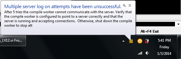
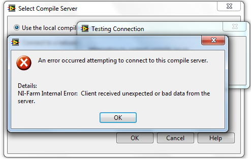
Internal error OR-farm - impossible to compile the FPGA VI
Hello!
When I try to compile any FPGA VI with LabVIEW2013 or 2012 SP1, I get the following error:
"Year error occurred trying to connect to this server compilation."
Details:
Internal error OR the farm: Client Server received unexpected or bad data. »
Intermediate files are not generated, the error message appears immediately after I have select build of build specification or I click the run arrow.
I use the local server for compilation.
The equipment I use: CompactRIO Evaluation Board - SbRIO9636, DELL laptop, Intel core2 Duo T5800, 2 GHz, 3 GB RAM, Windows 7 Ultimate 64-bit, SP1.
The intermediate files CAN be generated without any problems if I select in the menu. If I run the FPGA application compile worker, a ToolTip message specifying that "FPGA compile runs", but after a few seconds, another message appears: newspaper several attempts were unsuccessful - please see attached images.
At first, I thought that my firewall (Comodo 6.3) is the reason for this, so I disabled it but nothing changed. Then I tried to fix LabVIEW FPGA and XILINX tools with the firewall disabled but din do not solve the problem. I tried with LabVIEW SP1 of 2012 and 2013.
If you have any suggestions, please let me know! Thank you!
We would like that you try to reset the NIAuth database by following these steps:
1. go to Windows Services (Bring up Windows with Ctrl + Alt + Delete Task Manager, click the Services tab, click the Services button at the bottom right of the window.
2 stop the NI Application Web Server and NI System Web Server services in this order (right click, stopping service and select).
2 backup, and then delete all the files under %PROGRAMDATA%\National Instruments\NIAuth: registry.bin and commitmark.
3. run NI System Web Server and NI Application Web Server services in this order.
4. navigate to http://localhost:3580 / connection of an IE on the local computer and try to log in with username "admin" and password empty. Succeeds, the server will return one signed in as: message from the admin.
After you follow these steps, try and connect to the FPGA compiler, and then let me know what are the results.
-
Cluster for the FPGA reference constraint
I have a cluster of clusters. One of the internal piles went 25-29 items, but I forgot to update several of my Subvi reflect. I remember before when I did, I got a broken line not executable VI, but now the result is a constraint. You can really force a cluster with multiple items to a cluster with fewer items? My outdoor group consists of some FPGA with clusters of register references.
Hi Adams,
FPGA reference is the special data of type "FPGA dynamic reference", which includes a cluster of records, elements, and associated with the referenced FPGA personality FIFO dynamically. Dynamic data types do not follow the same rules of coercion expected of them a defined data type statically to follow. The dynamic nature of reference FPGA son allow wire any FPGA reference in the entry of an order of read/write, regardless of whether the control of read/write was created explicility for the FPGA reference. This makes it much more practical FPGA programming.
-
Hello
I'm developing an app for the compactRIO systems. I want to implement a heartbeat in the FPGA code that detects if the host vi gave up. I also want the FPGA vi at the stop with a stop of the host vi command.
I implemented the heartbeat signal within the host vi and the heartbeat counter is located in a loop of the single cycle timed (SCTL) in the FPGA vi. However, I have other loops while in the FPGA vi (b/c I/o analog are not compatible with the SCTL) and so I need to stop several multiple loops with a stop order from the inside of the loop cycle timed (by opposition from a user input, what you can do with a local variable).
As I have now, when I download and run the code to my compact goal of RIO, and I abandoned the host vi (and not by pressing the stop button), the code in the SCTL stops, but on the other the loop is not. Can anyone help?
Greetings Andrew P.
I took a quick look at your code, and while I'm not completely sure of the cause of the behavior that you are experiencing, I noticed a few things in your FPGA code. First of all, it seems that you use an appropriate method to report the other loop the SCTL is stopped due to the delay of heartbeat. Secondly, it seems that the logic around the heart rate monitor can be a bit off. Currently, you are taking the current value of the entry of Heartbeat/command and comparing it to the value returned by the shift register using a not equal to vi comparison. This allows to detect a change in the status of this entry if the shift register is providing the value of previous to this entry. However, it seems that you take the value of the comparison is not equal to to fuel the shift register, rather than the current value of the control of heart rate. What happens if you change?
Kind regards
Michael G.
-
The FPGA IO corresponds to which C-series e/s?
I have a PXI-7813R with connectors 0 and 3 connected to a chassis with modules of series C in them (9474, 9205, 9206 and 9423). I want to know that I/O corresponds to what e/s on these chassis.
As far as I know my FPGA project (which was written not by me) are the channels of each module of the series C are used, but I don't know what DIO channels they correspond with on the FPGA. For example, I can use the 9205 channels 0-31, but that channels 68 connector 0 of FPGAS which corresponds to?
Does anyone know how to tell you this? Thanks in advance.
joedowdle wrote
I want to know that I/O corresponds to what e/s on these chassis.
Why do you ask that? When you use Connector0 to the expansion chassis, the Connector0 IOs are more available in the project, on the contrary, the expansion module chassis and can be configured as explaind here. Also take a look at this thread.
Christian
-
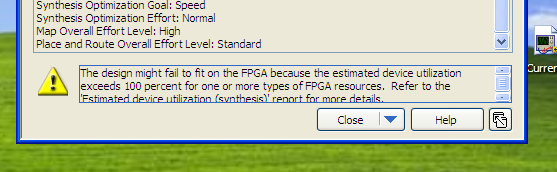
Failure of compilation of the FPGA target
Hi all
I met a problem when I tried to compile my target FPGA VI. Failed to compile for some reason any to halfway after start of the compilation. I post a few screen shots of the labview error information.
What causes this problem? How could I solve this problem?
Thank you very much!
Kind regards
masterwho
Also you have large networks on the Panel before the FPGA VI?
Or is there the great paintings inside the code?
If you can, put a piece of your code.
-
Entered digital high frequency to the FPGA could not be detected OK
Hello
We want to connect the CMOS camera with PCIe-7842R with SCB68 box to analyze the image in the FPGA. There are PCLK (pixel clock) signal (36 MHz) and 8 bits of data.
On the 1st, we write a test program to ensure that we can detect the PCLK correct which is attached as program.png. The program is very simple there is a loop timed with 80 MHz, which should be enough take 36 MHz signal. If the value of 8000 "Digital 2", we should have 3600 (+ -1) like "digital." The reason why we (+ -1) is that we have no synchronization, is supported in this test program. And we can get the right result in this configuration.
2nd part, connect us data to 8-bit on FPGA and we get a wrong result of PCLK. Even connect us only 1 bit (which is labeled as DIO1 program) data, the PCLK is disturbed, and we can't find out why. The configuration of the connector is attached as connector.jpg.
We tried to make 2 very distant digital signals, but are still not. We tried to change the cables connected between SCB68 and FPGA of SHC68-68-RDIO cable for SHC68-68-RMIO cable because we think she may have better armor. We have a better result but still bad.
Now, we put "Digital 2" 8000 and we have about 3400 ~ 3500 as 'digital."which is false.
Does anyone have advice or commands on this problem? I'm very appreciate your kind help.
Thank you.
Maybe you are looking for
-
Re: Satellite A500 - Digital Tuner DVB - T will not find channels
Hi all I recently bought a Satellite A500-02J. Im having problems trying to receive digital television with its built-in DTT tuner.When setting up through Windows media player everything is ok and said that the tuner is fine and set up correctly. But
-
Halo 2 do not start Windows 7 Ultimate
Halo 2 does not work on Windows 7 Ultimate. The problem is Microsoft Live Gaming. It still works fine for Red Faction Guerrilla. I tried stuff on the Microsoft site, but nothing helped. Sorry for my English!
-
Windows Live Messenger will not connect automatically, even if the correct boxes are checked.
Windows Live Messenger (WLM) will not connect automatically, even if the correct boxes are checked. WLM signs component snap perfectly when the Connect button is used, but simply refuses to connect when the computer starts. It happened once before bu
-
Guide to EA4500 of non-existent?
Just went looking for a guide to the user for EA4500 see: * virgins "Downloads" tab at http://homesupport.cisco.com/en-us/support/routers/EA4500 * Error "page not found" HTTP404 at http://homedownloads.cisco.com/downloads/userguide/EA-Series_UG_Full_
-
HY guys one last question so don't bother me. The direct watch is also resistant to scratches and water resistant or just the phone... Thank you...