[Labview FPGA]: block of memory use Xilinx HDL integration node
Hello
In my project, I would be developed my own VHDL module and integrated in my project of LV FPGA with a knot of integration.
But for an evolution of my code, I wonder if it is possible to use in my own code VHDL, Xilinx library (as a block of memory).
Thank you.
You can use any Xilinx IP (or IP and others) in your external code. For example, if you generate a block of memory using block memory generator you can instantiate this IP in your own VHDL.
Tags: NI Software
Similar Questions
-
Move from LabVIEW FPGA block of ram address to node CLIP?
Hello
I need to pass an index memory RAM of LabVIEW FPGA block to a CLIP node to the node CLIP to have access to the data in the BRAM. The node of the ELEMENT contains an IP address that we developed and the IP address is the use of Xilinx BRAM driver to access data. I guess that we need to move the physical address of the BRAM to the ELEMENT node.
Is this possible? If so, how? If this is not the case, what would be an alternative?
Thank you
Michel
If I understand you correctly, Yes, you should be able to use the memory block of the Xilinx pallet Builder in LabVIEW FPGA and in the loop of the single Cycle, connect the ports of this block signals CLIP exposed by the IP of your colleague. You may need to tweak/adapt some of the signals slightly to the LabVIEW data flow.
-
Use of FIFO memory on two areas of clock (Labview FPGA) block
Greetings!
I'm developing an application on the FPGA of the vector signal OR 5644R
transmitter/receiver. I have two loops single-cycle timed: a 40 MHz making a convolution
and writing a FIFO memory block and the second at 120 MHz (sample clock)
who reads from block FIFO memory and uses the following values
interpolation...Under what circumstances is it permissible to use a FIFO memory block to transfer
values of a loop from 40 MHz to a loop of 120 MHz (sample clock)?
The reason I ask the question, it is that the compilation of my code repeatedly of not
reported the error below:ERROR: HDLCompiler:69 - "/ opt/apps/NIFPGA/jobs/J9k7Gwc_WXxzSVD/Interface.vhd" line 193:
is not declared. I share for everyone's reference, screenshots of my code which is an extension of
sample 'Project streaming VST' given in NI5644R. A brief description of attachments is
given below...
1. "Top_level_FPGA_part1_modification.png": in a loop SCTL 120 MHz, a sub - vi bed FPGA
go a block FIFO memory... In fact, the reading is actually made when entry
"read_stream" is activated... (see details in read_from_fifo_true_case.png)
2. "Top_level_FPGA_part2_modification.png": a 40 MHz SCTL, wherein is a subvi FPGA
called to write the output of convolution to block FIFO memory.
3. "target_respone_fpga_block_FIFO_modification.png": an output of a convolution filter is
written in block FIFO memory each time that the convolution output is available...
'ReadBlockFIFO' VI (circled in Top_level_FPGA_part1) is invoked in a 120 MHz SCTL.
4. "read_from_fifo_false_case.png": when the input "read_stream' of this vi is false,
data transfer memory FIFO of block to a different FIFO ('generation filter") takes
place.
5. "read_from_fifo_true_case.png": when the "read_stream' is set to true, the data is read in
'Filter generation' FIFO and spent on the chain of later interpolation to the
120 MHz SCTL...
I hope that the attachments give enough clarity to what I'm doing... If we need
For more information, do not hesitate to ask...
Kind regards
S. Raja Kumar
Greetings!
I think I understand the problem... The error probably occurs because a DMA FIFO
(FPGA host) is playing at 40 MHz, and it is checked for the number of items in a loop
120 MHz... It is not captured by the "pre-processing" by the labview FPGA, but by the Xilinx
compilation phase synthesis tool.
A lesson I share, is that if you observe this kind of problem, watch if there is incompatibility
in the areas of the clock to access a FIFO...
Kind regards
S. Raja Kumar
-
CPU register accessible in LabView FPGA FlexRIO
Hello people, I wonder if it is possible to get the following behaviors of Labview. I think that it is not.
Description of the system: application of CVI which communicates with SMU FlexRIO via controls and indicators.
Problem: The design of a CPU-FPGA interface specification which lists the "books" as a combination of reading and reading/writing-the bit fields.
Example:
According to the specification, there should be a 32-bit register. 31: 16 bits are read-only, and 15:0 bits are read/write, from the perspective of the CPU. In the world of labview, I would just do a uint16 control and indicator of uint16 and do with it.
However, to meet the specification (written for microprocessor buses) traditional, a reading of 32 bits of an address should read back the full content of the 32-bitregister to this place (implemented as flops on the FPGA, with appropriate memory within the FPGA device mapping). In the same way a 32 bits of an address entry must store the values in this registry (properly masking wrote at 31: 16 bits within the FPGA device).
Is it possible for me to have a unique address (basically, a component unique labview block diagram) that will allow me to accomplish this behavior? It seems to me that the only solution is to pack my records with bit fields that are all read, or all the read-write in order to register in the paradigm of labview. This means that the spec should go back and be re-written and approved again.
Thanks in advance,
-J
Thanks for the detailed explanation. I am familiar with the reading and writing in the FPGA registers - I did a lot of work non-LabVIEW recently with an Altera FPGA. I haven't, however, used the CVI to LabVIEW FPGA interface, I only used the LabVIEW interface. I'm not sure if your question is about the CVI, LabVIEW FPGA interface or both.
JJMontante wrote:
Thus, a restatement of my original question: y at - it a mechanism with the use of indicators of controls where both the FPGA AND the CPU can write to the same series of flip-flops in the FPGA? If I use an indicator, the FPGA can write to the indicator, but the CPU cannot. If I use a control, the CPU can write in the control, but can't the FPGA. Is this correct?
On LabVIEW FPGA, a control and indicator are essentially identical. You can write a check, or read a battery / battery, using a local variable in the FPGA code. It is common to use a single piece of front panel to transfer the data in either sense, and it's okay if it's a command or an indicator. For example, a common strategy uses a Boolean façade element for handshake. The CPU writes a value to a numeric control, and then sets the value Boolean true to indicate that the new data is available. FPGA reads this numerical value, and then sets the Boolean false, which indicates the processor that the value has been read. The LabVIEW FPGA interface (side CPU) covers also all elements of frontage on the same FPGA whether orders or the lights--they can be as well read and written.
That answer your question at all?
-
LabVIEW FPGA failure with compiler Xlinx?
I'm in LabVIEW FPGA 8.6 with NOR-RIO 3.0.1 (to 8.6). When I compile a simple program, I get the notorious:
«Error starting compile step: make sure that a compatible version of Xilinx tools is installed in the location specified in the setup of LabVIEW FPGA.»
I checked the FPGA compile server and I ran the utility fixTlink.VI with no improvement. This produces two identical PC, neither one having a FPGA installed card.
Any ideas?
After further analysis, the problem was to be in our facility in LabVIEW FPGA 8.6. Using the correct Installer of NEITHER solved the problem.
This thread is now resolved.
-
Cannot find the HDL Interface node
I have MyRio and LabView 2014 with all modules installed and updated to date.
Xilinx 2014 is also installed and I can compile for FPGA.
However, in the block diagram I find interface HDL node for the import of VHDL code. As see you in the second screenshot.
How can I solve this problem?
There are no node integration IP in 2014 of LabView. Use instead the HDL Interface Node.
Yes I used the HDL Interface Node and it has worked very well.
-
FPGA block memory and Timing FIFO
Hello
I am trying to access the data of the memory block and a FIFO, both having an equal number of elements.
I'm trying to access the data must be coordinated with the waveform of a block of Xilinx, I use to deal with the elements of the FIFO and the memory block.
My block of Xilinx has a 3 clock offset cycle and one without a clock cycle lag, which can lead to my use of knots of late.
My question is, the output of an element of a FIFO occur in a clock or a clock set cycle? Also, I am aware that there is a delay of the output clock cycle
block of memory to hold data into account initial reading, which will lead to my choice of offset of 3 clock cycle. Just a handful to decide how much to delay the nodes to use.See you soon
Hi RichieA
If the function or if it is a FIFO, or a memory block is inside the recycled then timed loop function and of all that is on the inside must be executed in a heartbeat. Don't forget that when you compile you are actually programming and connect a gate array so when the compiler is running, it will try to create the FIFO or memory to be executed on a tick. If this is not possible, you should get an error in NI LabVIEW or in the compilation process. Here is a link with more information.
Single-Cycle timed loop FAQ for the LabVIEW FPGA Module
Concerning
R. Esteban
-
problem with a block of memory in labview 2009
Hi all
I have "ERROR: MapLib:979 - LUT4 symbol" during the compilation process (lots of errors like this), and I discovered that the reason of my problem is block of MEMORY.
To be sure that the problem is in this block, I did a very simple project in LabView 2009 (on FPGA Target PCI5640R) only with the use of this block you can see in the photo, as well as in file test_memory block.lvproj attached link: https://www.dropbox.com/sh/u87f1oihelmm4dq/Jo_6-bICSf
I have a problem with compiling VI with this block, and I have so many errors like:
ERROR: MapLib:979 - LUT4 symbol
"window/Thatcher/n_00000036/nSCTL_00000013_00000014/n_000000A3/cOutLoc<0>1.
(output = window/Thatcher/res000001ed_wi<2>) is the input signal
"window/Thatcher/res0000020d_wo<1>" that will be deleted. See Section 5 of the
Map a report file to find out why the input signal will become conveyors.or
ERROR: MapLib:978 - LUT4 symbol
"window/Thatcher/n_00000036/nSCTL_00000013_00000014/n_000000A3/cOutLoc<23>1.
(output = window/Thatcher/res000001ed_wi<25>) is an equation that uses
input pin I2, which no longer has a connected signal. Make sure that all the
the pins used in the equation for this LUT are signals that are not cut
(see Section 5 of the report file map for details on which signals were
adjusted).Entire report, you can see in the file report.txt on the attached link.
I would appreciate if someone could take a look at my problem with simple project and suggest me a solution.
I'm really stuck with my biggest project which need to have this memory block.
I'm looking forward to hear from you,
King looks
ING. Damir Hamidovic
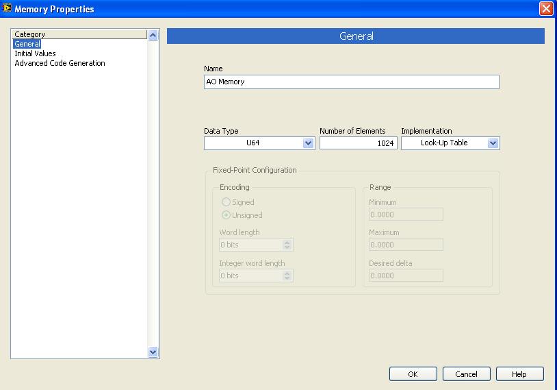
Hi all
I find a sollution to my problem.
In memory-properties-general-setting up, I changed the block to look up Table memory, and I compile memory.vi and run it successfully.
I did change as you can see on the picture:
Just, can you tell me is it all "bad properties" and limits the use of this type of memory (Look up Table) of the implementation?
King looks
-
Model a block synchronous dual-port RAM with LabVIEW FPGA
This question caught my attention recently.
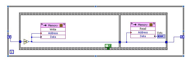
I am trying to model a particular design element called "RAMB4_S8_S8" with the LabVIEW FPGA module. This element is a block synchronous dual-port RAM allowing simultaneous access to two ports independently from each other. That being said, a port can perform read/write operation to this RAM while at the same time, the other port might be able to do the same thing. There are two opportunities of possible port conflict, however. The first is when both ports are trying to write to the same memory cell. The other scenario is when a port writes in a cell memory while at the same time the other port reads from it. Other than that, everything should be a legitimate operation.
In order to reproduce this I select memory block that is integrated into my FPGA target. An interface is configured to be the playback mode, and the other is set to write fashion. For the option of arbitration, I let the two interfaces to be "arbitrate if several applicants only. Then I got a compiler error when I tried to run my FPGA code for this model in a SCTL. The error message is something like "several objects to request access to a resource through a resource configured with option interface" arbitrate if several applicants only ", which is supported only in the single-cycle Timed loop if there is only a single applicant by interface.
This error goes away if I replace the SCTL with a simple while loop, but not what I would like to implement. So I wonder if there is a better solution to this problem, or is it just the limitation of the LabVIEW FPGA module.
Thank you.
Yes, you can use a form of conduct to perform the operations you want in the generations clock cycles, but all the code is inside a single SCTL. Basically, read the first address and storing in a register in a single cycle and then read the second address in the second clock cycle. This would allow you to two readings of valid memory every clock cycle 2. I have included a crude extract to illustrate the concept. The case selectors are identical with address A being connected to the memory in the true case, B in the case of fake address. Your biggest model memory dual port will be intact, but it will operate at 1/2 rate.
Take a look at the white paper that provides more details on the construction of memory:
Data on a target FPGAS (FPGA Module)
The ball on the memory block indicates that memory block double port cannot be applied in a configuration of reading, which is a double ROM. access read/write port must be imitated with custom code.
-
Exactly how memory works in Labview Fpga
I use a PXI 7853 and me for the last few days I've been playing with the help of blocks of memory in the FPGA.
Now, I'm relatively new to Labview FPGA programming and this is why I would be grateful if someone could provide me with some clarification on the following points:
(a) given that I work on the development host computer when I initialize memory with the ability to use a memory initialization VI then how does exactly in the backend. What I want to ask is, when I change the values of the memory in the computer development and then compile the FPGA VI in the Board of Directors, what is data memory are brought in the FPGA. If this is the case then in what form are the details initially registered in the development computer.
(b) is it possible for me to use the initialization method VI to change memory n valuesi while the FPGA VI is running. If this isn't the case, then it would make a difference if I stop the VI and then change the values using the Initialize method. Who would actually reflect on the FPGA or should I have to re compile the FPGA VI whenever I change memory values in the development machine, using the "VI initialization method (which is available as an option for us do a right-click on the block of memory in the Project Explorer window).
I tried test with simulation of FPGA VI and found that when I try to change the values of memory by running VI initialization. a pop up that says that it is not possible that the FPGA VI is still in service is delivered.
Any light on this or advice with links would be much appreciated
See you soon
sbkr
sbkr wrote:
(a) given that I work on the development host computer when I initialize memory with the ability to use a memory initialization VI then how does exactly in the backend. What I want to ask is, when I change the values of the memory in the computer development and then compile the FPGA VI in the Board of Directors, what is data memory are brought in the FPGA. If this is the case then in what form are the details initially registered in the development computer.
When you compile the FPGA VI, he will understand the values used to initialize the memory.
Are asking you what happens if you run the VI FPGA on your development computer, and your FPGA VI, written in the memory block, the new values are included when you compile the FPGA VI? No, these values will be lost. The values contained in the bitfile are the values you used to initialize the block of memory, as defined in the memory properties dialog box. The initial values are saved in the LabVIEW project file and the definition of memory block.
sbkr wrote:
(b) is it possible for me to use the initialization method VI to change memory n valuesi while the FPGA VI is running. If this isn't the case, then it would make a difference if I stop the VI and then change the values using the Initialize method. Who would actually reflect on the FPGA or should I have to re compile the FPGA VI whenever I change memory values in the development machine, using the "VI initialization method (which is available as an option for us do a right-click on the block of memory in the Project Explorer window).
You will have to recompile the FPGA in order to use the new initialization values, because these values are part of the bitfile FPGA.
-
Zip file and iso LabVIEW FPGA Xilinx tools 12.4 Module is broken
I downloaded the two zip file of LabVIEW FPGA Module Xilinx tools 12.4 and iso image file three times to make sure that both files are broken and can not be installed!
The size of the file is so large about 3g. It would be better to double-check before you download on the Web site.
-Very well,.
The download is complete and the standard Windows Extraction tool worked, WinRAR worked and 7Zip worked (and no, I don't know why, I installed all). I did download a wireless network that does not have direct access to our internal servers, it should therefore be a test valid. If the link I provided above was not that you used (probably isn't, because it is not an ISO option), could you please provide me with a link to the page that you used so that I can test and repair? In the meantime, the link above should work for you.
-
Drivers Xilinx/Multisim and Labview FPGA
Where can I find drivers for my FPGA OR if I use Multisim/Xilinx and NOT of Labview? All the links I found are Labview be installed. However, the explicit manual FPGA indicates that you can use Multisim/XIlinx ISE in place.
OK, I tested just outside. The Driver of LabVIEW 2013 DEFB contains 2 separate components, the driver and Module FPGA support. If you run this installer, it won't check if you have LabVIEW FPGA installed unless you check the box for LabVIEW FPGA support.
I can change the text in the Installation Instructions to read "LabVIEW FPGA 2013 is required to install the LabVIEW FPGA Module Support component installation".
-
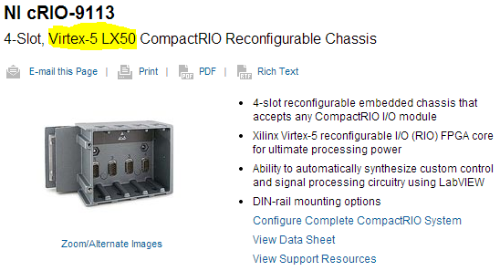
Download NI LabVIEW FPGA Module Xilinx Tools 10.1 2013 problems
I'm trying to download the Xilinx tools 10.1 to use with a chassis 9113 in LV2011. Based on this white paper, that the compiler below should work perfectly. The problem is that I can't seem to download all the way.
I can't seem to cross ~ 336MB using the standard or the downloader OR. Any ideas? Does anyone else have this problem?
http://www.NI.com/download/LabVIEW-FPGA-Module-2013/4249/en/
Thank you
-PBD
Well well... on the good side of things, you don't want 10.1 anyway!
Virtex-5 LX50 FPGA<- requires xilinx="">
10.1 is only for devices FPGA Virtex-II! (.. .after LabVIEW 2009 it was, just for all of you who read this know).
so... try this link: http://www.ni.com/download/labview-fpga-module-2013/4248/en/
-
LabVIEW FPGA: Compilation failed due to an error of xilinx
I'm getting a 'Compilation failed due to the error of Xilinx' you try to compile the code in LabVIEW 2013.The code has successfully compilated in labview2012. Any suggestions on what is causing this problem?
Details:
ERROR: HDLCompiler:432 - "C:\NIFPGA\jobs\THY4t7n_z6im2K7\NiFpgaAG_0000003a_SequenceFrame.vhd" line 29: Formalhas no real or default value.
INFO: HDLCompiler:1408 - "C:\NIFPGA\jobs\THY4t7n_z6im2K7\NiFpgaSetOutputDataEnable.vhd", line 37. cparametersignal is declared here
ERROR: HDLCompiler:854 - "C:\NIFPGA\jobs\THY4t7n_z6im2K7\NiFpgaAG_0000003a_SequenceFrame.vhd" line 21:Unit ignored due to previous errors.
File VHDL C:\NIFPGA\jobs\THY4t7n_z6im2K7\NiFpgaAG_0000003a_SequenceFrame.vhd ignored errors
-->Total memory use is 204688 kilobytes
Number of errors: 2 (filtered 0)
Number of warnings: 4 (filtered 0)
Number of news: 0 (0 filtered)"Synthesize - XST" process failed
Compile time
---------------------------
Introduction date: 2014/2/26 18:15
Date recovered results: 2014/2/26 18:17
Waiting time in the queue: 00:06
Compilation of time: 02:02
-PlanAhead: 01:16
-Generator kernel: 00:00
-Synthesis - Xst: 00:35Hi guys
I think I can give you a helping hand on this.
I have the same problem when I'm working on the Tutorial (2013) exercise 2 with Rio evaluation Kit.
You can try one of the following option.
Solution 1.
1. in the VI package manager.
Select 'Tools '->' Options'-> "General '->' package Installation"-> Unchecked 'mass Compile screws after Installation of the package.
Solution 2
1. in the VI package manager, uninstall the driver LCD
2. unchecked "Mass compile screws after Installation of the package" (see Solution 1)
3 reinstall the driver of the LCD screen.
Mine did after Solution 2 and the compiler works.
Hope it will be useful for you guys.
Thank you
-
Simulate the sine wave using LabVIEW FPGA with NOR-myRIO and display in real time
Hello
I'm relatively new to LabVIEW FPGA. I am trying to test (and later apply) controllers high speed on myRIO.
At this point, I'm trying to simulate the sine wave from 1 to 10 kHz using Sinewave generator VI express. I also intend to display the sine wave on the time real (RT) using FIFO. However, I had a bit of trouble to understaing various synchronization parameters.
1. how to encode information about the sampling frequency generating sine wave? (The side FPGA vi requires only the frequency of the signal and possibly phase and does not rate update lines)
2. how to estimate the number of items in a FIFO? (that is, the relationship between the rate of updates to loop (RT), the signal frequency, sampling frequency and the number of items in the FIFO)
It would be great if we could share a very simple program (side host and target) that did something similar.
Thank you
MILIN
Milot,
I think the problem is the type of data in your FIFO. Your FIFO is configured to use a data type of I16. The problem is the number, it displays only ever will be-1, 0 or 1. To resolve this problem, you must send the sine wave as a fixed point data and convert it to a double on the side of the RT. This should significantly improve your resolution.

Maybe you are looking for
-
Central Seagate NAS - "Invisible" Time Machine backup
Running OS X El Capitan (10.11.3), have a central Seagate NAS connected to the same network. Struggling to locate/mount the Time Machine "partition" of the NAS using the Finder, even if the NAS works more or less perfect otherwise. For example, I hav
-
Original title: in my desktop screen. the BSOD appeared... Hello everyone, While to my desktop screen (don't remember if I was doing anything however), the BSOD appears, indicating the system stopped to avoid any damage occurs. The following was then
-
Not available on internet MediaHub
Hi all This is the first time in a year, I need to seek support as im out of ideas how it is possible. Using Linksys WRT610N with port 21 (FTP), 80 (HTTP) redirects. 443 (HTTPS) and 9000 to 192.168.1.5 local IP which is the mediahub. Locally, I can a
-
Walkman 8.4.A.5.4 Force closed
Today, once I opened the Walkman, she jumps through the window and showed that "Unfortunatey, walkman has stopped." Has anyone had this problem? I bought Xperia song due to its applications of Walkman, Sony, please help solve this problem as soon as
-
Message "Install the program as an administrator"
Just a curious point. Sometimes, I get a message saying "this program must be run (or installed) as an administrator." As I am an administrator on my own computer (in fact the only one) why windows sometimes mean? It is not a vital request just a poi