Module e/s NI 5761 clock compiled 0 to 100 MHz in single/multiple Sample CLIP examples of projects
Hello
I was trying to wrap my head around the CLIP sample NI 5761 Multi (v4.1.0) because the CLIP provides 250 PSM data, but the IO module requires a clock of 200 MHz. I think, ' NOR should handle the conversion of the clock, fine, but I hope that the diagram is running at 125 MHz... otherwise I'm really confused "so I look at configuring the clock Module e/s in
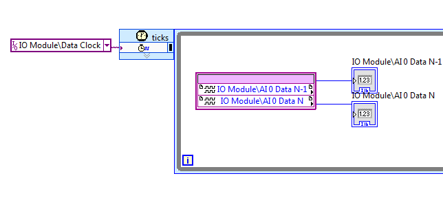
I checked the target 7965 in NI 5761 single sample CLIP\NI 5761 - unique CLIP.lvproj and IO Module clock 0 sample was compiled for 100 MHz there as well. I do not understand the difference between the flow of data and the selection of clock 200 MHz IO module, and it would be nice to understand it, but not necessary. Also, I don't understand the difference between data rate and the configuration of the Module e/s 0 clock that drives the SCTL that contains the node IO. I understand that to move forward. Thanks for any help, Steve K The CLK200 in the selections of the clock is used to excite the parts of the fixed logic that are internal to the CLIP. Some CLIPs FlexRIO may only require a CLK40, this one requires a CLK40 and fixed a CLK200 to properly perform its logic. Thus, it seems that everything is ok in regards to that. Unfortunately, the example incorrectly uses IOModClock0. The SCTL AI IO node resides in should use a resource of the clock that says "Data Clock. We've updated the examples in more recent versions of the pilot, but you seem to be using a version of the driver where a CLIP that uses the clock of data is the latest available for the 5761 CLIP, but the example has not yet been udpated to use. Tags: NI Products How to get a regular clock (100 MHz, 10 MHz to 20 MHz) of the NI 4462 PCI? Is it possible to extract a regular clock, high frequency of the 4462 OR? I need to synchronize with another card (a PulseBlaster), which requires a 100 MHz clock: every card can be the main source, but they must stay perfectly synchronized. (Both cards have on-board crystal oscillator modules of 100 MHz; one of the PulseBlaster is nested, would be so easy to connect a source external intead) I use the PCI version, so the star PXI 10 MHz clock is not available. The 10 MHz or 20 MHz clocks that DAQmx usually exports seem not to be available for routing on this device. I can't use the Sampleclock, because it is variable (~ 25.6 MHz, changing with sample-freq) and because it is not active when the 4462 is actually measurements. In addition, this clock must be either 100 MHz, or a whole simple fraction of it (e.g. 10 MHz, so that a PLL can re - generate the 100 MHz). At the present time, the best option seems to be to solder on the 4462 output pin quartz oscillator - but it's a really ugly way do... has anyone had an experience to make relevant changes? Is there a better place to connect to? I would prefer to use the RTSI bus connector, but despite tempting advice in the documentation, it seems not possible to get out of the 10/20 MHz master time base: there is an axis called RTSI7/RTSI_OSC, but it is a permanent decline. Thanks for your help. Nick Dear, Thanks a lot for your help. As you say, this confirms what I already knew. But we really need keep everything in harmony. So, here is what I did, which should hopefully help someone else in the same position. The circuit is very simple, using a FIN1001 LVDS line driver. It is a SOT-23 package. Connections are the following: * Din connects to the output of oscillator 100 MHz (TC0-2104, pin 4). * Gnd connects to the Earth (C210, lower) * + 3v3 connects to the more accessible place, that TCO-2104, PIN 6. [The 3V3 regulator is on the back of the map] * FIN1001 food is decoupled with a 0.1uF adjacent capacitor. * Dout + and Dout-are connected to a short (30cm long) of the unshielded, twisted pair made of wire 0.7 mm PTFE. (Z ~ 110 ohms) Photograph is attached. The SOT-23 package is physically secure, with a tiny drop of cyano, C210 and mounted on his back. The receiver uses a FIN1002 receiver, finished with 100 ohm twisted pair and uses a 74VHC04 to convert 3.3V 5V TTL. It is mounted on a 14 pin DIL socket, to plug directly into the socket on the other card PCI which normally has its own oscillator module. Result: everything works, and I have a 100 MHz clock available to drive the other timing card. Module MT FSK. VI, too slow: 5 seconds to generate a single waveform. Hi guys RF OR,. I have problems of bigs with the module MT FSK waveform. I'm trying to generate RF signals, based on sending a stream of input bits to 544 bits with a rate of 8.8 KHz modulation, with a frequency of 15 KHZ deviation and the frequency of 433.92 MHz. The problem is that it takes 5 seconds, the wave must be generated, that is too long. I noticed that by changing the rate of modulation (inreasing it) decrease processing time which is normal, but I send with a rate of modulation of 8.8 KHz for my receiver to be able to 'catch' the signal. Is it possible to decrease the processing time? Many thanks in advance Hi all I found a solution for my problem... An unknown program is repeatedly reproducing and using up to 100% of cycles CPU. This can be cured? Windows 7 Edition home premium Hi johpata, Explore process will help to identify the offending process and perhaps kill him if you wish. Sysinternals 'Process Explorer. http://TechNet.Microsoft.com/en-us/Sysinternals/bb896653.aspx Tutorial of process Explorer. http://www.YouTube.com/watch?v=EfxI9NtUa8U Good luck. Upgrading RAM on Satellite L650 - 10H Hello and one more thing, it is I can't find any data on this module in this site Hello You can update the RAM up to 8 GB, but as much as I know bus Frontal (FSB) is limited to 1066 Mhz Even if you want to use the 1333 Mhz modules, the FSB would be clock speed to the 1066 Mhz is not worth to use 1333 Mhz as this seed would not be used. Crosstalk channel PFI, error Code:-201314 Hello world I would like to make several synchronized outer edge count the spots on a NI PCIe-6353. The problem is that I get crosstalk of impulses between the channels of the PFI, leading to some sample clock pulses and possibly error-201314 misinterpreted: "Multiple sampling clock pulses have been detected in a period of the input signal. Use a sample clock rate that is slower than the input signal. If you use an external sample clock, ensure that this clock signal is specifications voltage level and jitter and seedless. » I count the pulses of the APDs, they have a height of 5 v, width 20ns and a rate of about 1 MHz. My sync Signal has a frequency of 10 kHz repetition, the pulses are 5V high and long 50µs. When I start the measure, it takes only a few seconds until the mentioned error is displayed. I can also confirm it with the NOT-MAX, in "cash" pulses in my sample clock input channel even if there is nothing in annex (only the DPA on the meter channel). I tried the following combinations: connected to sample clock: 0, 5 PFI, PFI 1 PFI counter connected to: PFI0, 5 PFI PFI 8, PFI 3 they all failed except when I use the PFI8 as the only source of meter. In addition, the edges of pulse with a lowpass filter of depreciation or the addition of a resistance of 50 Ohms for the connector does not work. The connecting cable to the junction box is 0.5 m long. I tried the SCB-68 has and a BNC-2110 case without much change in behavior. Is there a way to better isolate the PFI channels, or are there channels which are better insulated from each other? Thanks for the help Fabian You can set up a digital filter on the sample line PFI clock to prevent noise to register as legitimate a sample synchronization signal (pulse Min set to something less than the width of sample clock but greater than the width of the pulse noise - 5.12 we we use built-in dividers and would probably be appropriate). If you want to troubleshoot the source of the noise itself, I would start with the scope of the sample clock line (the scope must be fast enough to pick up the pulses of 20 ~ ns if it is indeed the source of the noise). I guess that the problem is more likely to how signals are connected/set to land. Do not forget that the PFI lines on the DAQ card share a digital ground. Best regards Using the C-series SCTL DIO module with slower than the top level [FPGA] clock Hey all,. I'm running online research on a problem that I have a lot of success. I have a chassis with integrated FPGA, top-level 9030 clock 40 MHz. I have a NOR-9401 DIO C Series module plugged and the value that will be managed by the FPGA target. I need to count some linear encoders to exactly 10 MHz, no more, no less. They are periods and gives a result of such kind that if I oversample or underestimate, I get garbage. If I create a SCTL and assign a source of synchronization derived from 10 MHz, I get an error code generation who: "Node read e/s for DIO3 FPGA is used in a clock domain that it does not support. Areas of clock supported include: the clock of higher and clocks that have a rate that is a multiple of 40 MHz, for example 40 MHz, 80 MHz, 120 MHz and so on. » I tried several ways to work around this problem; First I tried just using a while loop with a loop set to 4 is ticking timer, but it then takes 9 clock cycles to perform the count for a reason any (although this code may compile in the SCTL without any problem). I then tried to use the SCTL with a constant of 'true' AS a hack for a 'timed sequence' framework-related, and that certainly has not worked. Are there any strategies or techniques, or settings somewhere to work around this limitation on the AID I need to taste exactly 10 MHz? I'd like to do this quickly in the software and get this rolling as soon as POSSIBLE. An image of the relevant section of the code is attached, I'm happy to provide you more things on request. Thank you very much! Maia Bageant Thanks for the reply! The problem ended up being a hardware problem based on how coders were connected. Now that I've fixed it, they're perfectly happy are oversampled. I guess my question is always legitimate to other applications, but not necessary for encoders a. Compilation of modules for an installed, but not running in the kernel? With LANG = C vmware-modconfig - console - install-all I can compile the kernel running modules. But how can I compile the kernel modules does not? Think about it. You can't unlees you start with the kernel that is not running. Hello I want PLL select my 5761 to PXI_CLK10 by setting the sample clock signal. I use the adapter with an SMU-7965. The Manual 5761 synchronization article leads me to believe that I can do this: "Reference, 10 MHz, external clock through IoModSyncClock." The subject of several CLIP sample 5761 in aid of FlexRIO gives me the value to write, "select the sample clock, 3 = sample clock internal locked to an external reference clock through IoModSyncClock". And
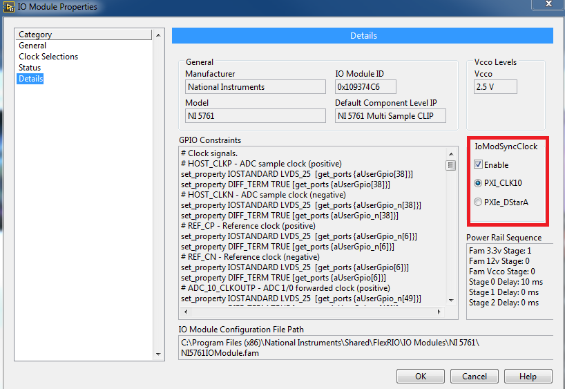
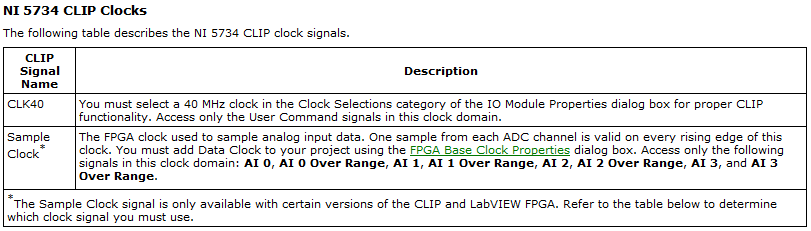
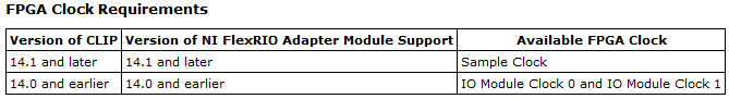
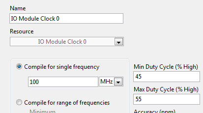
I'm missing how to get the PXI_CLK10 to IoModSyncClock. There is an explicit note in table 4 of the Manual of 5782 indicating, "the VCO internal locks to PXI_CLK10 through IoModSyncClock, which is available only through the backplane of the SMU-796xR NI devices", when the clock is set to the internal clock PLL on (IoModSyncClock). Perhaps the same applies to the 5761 even if they seem to have different options for overclocking? I don't want cable CLK10_OUT of the chassis at CLK IN on the 5761 (which seems silly). I don't want to use the API of Sync FlexRIO Instrument Development Library to PLL to backplane. Thanks for any help, Steve K You set the IOModSyncClock line in the FAM Propties page on the category details. By default, the PXICLK10 is automatically routed to the IOModSyncClk line. 5603 IF given NOR 5761/a. port Hello I have a composed of digitizer vector signal Analyzer 5622, 5603 frequency step-down converter and synthesizer 5653. To get to the point, I'm trying to synchronize the clocks of the ASB and the 5761. as well as the module of synchronization, Richie Hi Richie, It is possible to generate two different clocks, but you shouldn't need to. The best way to do it would be to spend the clock by Ref Out of 5653 for Clk synthesizer in the digitizer 5761. More information is found in the Starter guide for the SMU-5665. Replace just the 5622 by the 5761. The LO is usually set on a certain signal IF according to the RF input to output. I don't think there is a way to change this, but you can set your scanner to wait for the correct values. Concerning Understand how to set up and use a sample FlexRIO clock Hello Following this discussion on inputs glitching, I learned that I need to use the area of the sampling clock to read nodes to HAVE it in my 5734 OR. So I right click 'FPGA Target'-> "New FPGA Base Clock" and selected "IO Module clock 0". In general, I followed the instructions at http://www.ni.com/pdf/manuals/375653a.pdf Issues related to the: Hi FKSH, You are right that you must Access your e/s on the 5734 NOR in the area of sample clock: (this information is by using LabVIEW for the CLIP of 5734 OR) It is a clock Module e/s 0 or sample clock based on your version of the FlexRIO driver you have installed. Based on your statements, looks that you use LabVIEW 2014, so be sure to have FlexRIO 14.0 or FlexRIO installed 14.1. If you have FlexRIO 14.0 or earlier, the sample clock will be IO Module clock 0. If you have FlexRIO 14.1 or later, it will be the sample clock: (also of the documentation NOR 5734 CLIP in help) The only support for sampling rate is 120 MHz, unless you use an external clock CLK in and it must be between 50 and 120 MHz (see page 9 of the Manual). If you wish to purchase to 10 MHz, the best thing to do would be to sample the e/s to 120 MHz and then decimate the data by a factor of 12 (keep all 12 data points only and throw out the rest). Regarding the FIDL, I'm guessing that you're referring to the configuration in the properties of the clock: This configuration is not actually change the frequency of the clock. The compiler uses this value so that the logic can operate at the specified frequency, but the real clock is provided elsewhere (in this case, the FAM).
Finally, I saw error-61046 occurs more often because of the configuration of the internal clock. Make sure you use the clock on the right as the only cycle timed loop source as I mentioned above. In general, I do not recommend write directly on a 120 MHz indicator, as there are a lot of other logic that needs to be done in order to update the indicator. The data are sent to a domain different clock under the hood, so you can actually update the data and I suspect that there are some conflicts with the clocks. You also lose data as the host won't be able to read all the data before it gets crushed. Instead, I would use DMA FIFOs if you need all the data you acquire or to send the data to a different loop which will be responsible for the update of the indicator in a slower clock domain.
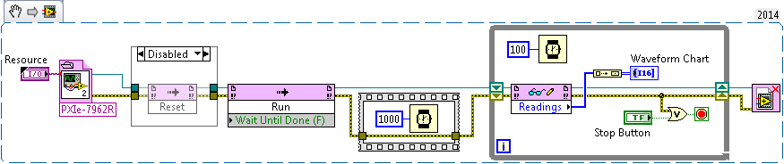
In general, I recommend always that the start-up of the examples in the Finder as a good place to check if the equipment works properly and as a reference for the correct configuration. Once you compile the code, you should be able to run it natively to acquire some data. "" "These examples will be under input and output hardware" FlexRIO "Modules e/s ' NI 573 X ' NI 5734. Best regards Hi, just got my new cRIO-9067. I have converted my project over the cRIO-9067 since the cRIO 9074. Same layout module, same engine, same scan code custom fpga, (hybrid mode). I have no problem of compilation for the 9074, which is a lower performance FPGA architecting the 9067 FPGA. The final timetable for windows compilation shows that the timing is respected for all clocks - 40, 80 and 120 MHz (I use a clock derived for some code sctl). During the end of compilation, during the phase of gen bitfile, I get the dreaded time violation. Investigation of the breach indicates that it is not the custom code, it is not schema components. One of them seems to be linked to the card series OR 9870 I in the chassis. Why? Is there anything I can try with the compiler directives for this problem? You would think that it would be easier to compile for the highest performance FPGAS... OK, don't ask me how I thought this output - to run I changed nothing else than this: feed the I/O node a reference FPGA of e/s instead of configure the node via the menu "link to. It makes no sense, but the compilation succeeded when I did this. I know it is because I created a very simple test VI in my project and made sure it does not compile without it. Question about 6674 t FlexRIO 7966R and Module AT - 1120 FAM DSTARA Hello I have a chassis SMU-1085 and following committees installed: Slot 10: Module of synchronization for the SMU-6674 t Slot 02: SMU-7966R FPGA Attached to the SMU-7966R FPGA is a module of adaptation AT1120. I'm trying to provide a clock of 125 MHz by the 6674 t the bottom of basket DDS output to power the clock DSTARA the SMU-7966R and then the module adaptation AT1120 as the clock of the DAC. GMac, Hello! There are three things that I think that in the combination will solve this problem. 1.) can not included it in your screenshots, but there is an extra step you need to do to use the DSTAR. The bitfile you are using must be respected with a parameter that indicates the FlexRIO use the signal DSTARA. 2.) also, what you see was a known problem that has been fixed in Active Techonologies (AT) last software update (version 1.8). While I'm not 100% certain, I don't think the example started to get has been updated so that it includes all the screws of the ATs software update. Similarly, the bitfiles provided with this sample would have not generated with the CLIP included in the latest version of the software.
I suggest the following:
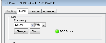
3.) generate a signal from 125 MHz of the 6674 t, not 124,98 MHz. The material is expected a 125 MHz signal. Dialog said 124,98 MHz with workaround for an odd present which was causing compilation failures. If you would like more information about this, let me know and I'll fill it in you read this post on the forum: http://forums.ni.com/t5/LabVIEW/7966R-DSTARA-Clock-and-AT-1120/m-p/2932916#M847692 I hope this helps! The CompactRIO Modules are not connected I'm currently developing a compactRIO, but modules are not detected in system OR distributed, Manager even after hitting refresh Modules in the scan engine. LabView is able to detect modules, but the code does not compile. Watching the memory usage in the Distrubted System Manager it shows that there is no available memory and he has no memory allocated. I tried to reboot the device, uninstalling and reinstalling the software, but nothing has worked. Any ideas of what I could do to try to fix it? Thank you! This was the tutorial I used to implement http://www.ni.com/getting-started/set-up-hardware/compactrio/assemble. He has got to work! I reformatted the compactRIO and reinstalled the software and that seemed to do the trick. Thanks for your help! For anyone who runs into this problem, I found the following documentation to be a good reference: http://zone.NI.com/reference/en-XX/help/370622K-01/lvrtconcepts/deploying_running_vis_rttarget/ I followed the steps described in the section "Troubleshooting steps" OR Scan Engine deployment. synchronization and clock cDAQ-9174 I have a cDAQ-9174 with chassis HAVE - 9205 OR 9205 HAVE - NOR 9219 DIO - OR 9401. "NOR-DAQmx allows the on-board clock routing synchronize acquisition or generation of data transactions. A single sync signal or a trigger can be shared between multiple operations on the same device to ensure that the data are synchronized. These signals is shared by the simple signals routing functions that allow connections integrated hardware DAQ. " (from http://zone.ni.com/devzone/cda/tut/p/id/6829) When I check the itineraries device in MAX tab' for chassis and c modules individually, I found many clocks with the Green blocks (direct Route). "Once a physical connection is determined, the NOR-DAQmx driver lets the user quickly and easily use this connection to synchronize operations". Now my question is how do you choose among these clocks available. What is the frequency of these clocks? The highest frequency the better? What is the difference between /Ctr0SampleClock, /Ctr0InternalOutput, /Ctr0Source, /Ctr0A? For example, why well/Dev1/I/SampleClock or Ctr0InternalOutput or of others, especially as a source for the .vi DAQmx Timing (sample clock)? Thanks a lot for your help Bing Concerning Hello NCLbingji, I think you mix instructions from the manuals of different material. The link you posted refers to the synchronization of several separate devices, while your cDAQ with its modules really is like having one device almost. You will find more relevant information in your manual of cDAQ chassis. For multiple devices, you indeed have a "physical connection", but with the cDAQ is not necessary. You set up these connections in the software in any way, and this should get the routing sorting at the driver level. Try to identify which channel will be your a 'primary', the one driving all others and synchronization, the value then asked SampleClock of this string as the rest (DAQmx Trigger.vi) trigger ('secondary') channels, then start all 'secondary' jobs and finally start your "primary" task This will trigger all tasks at the same time. Take a look at the attached picture, which is another application that I worked on, but I think this will help. I hope this helps. Kind regards Michael S. 32 Firefox will not start after a download. On windows XP sp3. Chrome and Iexplorer 8 will take place. Firefox will launch. Cannot run firefox.exe Pei either. Satellite Pro U400-G13 - "C++ Runtime Error" at startup Hey the Toshiba Forum users I just bought a Satellite Pro U400-G13I turned on and the auto install startet Windows Vista. The inexplicable to the computer.After the reboot, a toshiba program starts and requested a restart more.After that, I have a "C Upgrade of the T61p Widescreen processors Hi all I have a T61p a few years ago now and I look at improvements in spare parts. Currently, it is a 2.5 GHz T9300 Intel Core 2 duo, which I learned is a Socket P processor, named "Penryn", 800 MHz FSB. If possible, I would like to know of all the How can I get full control of all of my files and folders I really hate this version of Windows. but in any case, I would like to take full control of 'All files and folders on my computer' for access at any time without having to ask permission whenever I want to access. I installed a few programs I want t How/where can I view activity indicator when loading new records in listview Hello I would like to display a kind of activityindicator when I load more records into my view of the list... IE when atEnd struck in ListView:nScollingChanged(). My question is can I view the ActivityIndicator in the listview control itself or I vSimilar Questions
I have PSK1JE L650 - 10 H 00400GH2 with 4 GB 1066
I want to update 8 GB 1333
This module it supported?
dose the laptop has 2 springers to upgrade ram or more?
When I try to auto detect the module of your software in my laptop it does not find
I also a 6674 t connected to an atomic clock synchronization module and a card 5761.
Instead of going directly to the digitizer, I am currently trying foods I / data Q If the buck converter of frequencies at the Ch0 of 5761 card input (A/D)
in order to process the data immediately in the FPGA.
as I am able to get the number correct samples at a certain frequency of sampling to the 5761 entered.
What I need to do to exclude the digitizer and have the 5761 in lieu of the digitizer?
I'm quite new to using NI DAMA and Module synchronization tools in Labview, but I've included the VI I am trying to run on the host side at least for
a Visual idea.
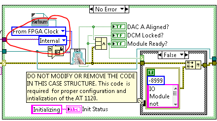
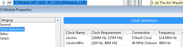
For my adapter module CLIP on the FPGA VI I have the clockin set to the DStarA Clock as shown below:
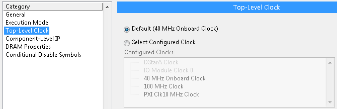
For my FlexRIO 7966R I have the toplevel clock set to the defautl 40 MHz onboard clock. I cannot use an external clock for this:
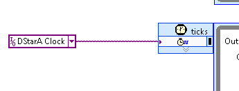
Then I have my SCTL clock set to the DStarA Clock:
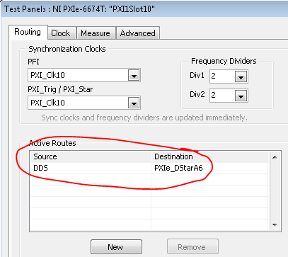
For simplicty sake, I am trying to feed the DSTARA clock using the test panel in NI Max with 6674T as follows. Becuase my FPGA is in slot 2 on the 1085 Chassis, I am feeding the 125 MHz DDS frequency to PXIe_DStarA6 based on the PXIe-1085 user manuel (http://www.ni.com/pdf/manuals/373712e.pdf) specified timing DStar lines:
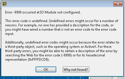
However, when I try and run my VI with all of these settings I get the following error:
Has anyone seen this, or can anyone advise regarding this? Maybe I'm using the DStarA lines wrong or something, but I'm not sure. Any help or suggestions from the community would be great!
Thanks for all your help!
-GMac
Technical sales engineer
NEITHER UK & IrelandMaybe you are looking for