Stability clock embedded FPGA
Hello
I'm looking for more details on the clock embedded to cRIOs stability (mainly 9076). Data sheet does not say much to that. So, what type of oscillator is used for the generation of on-board clock (40 MHz), how accurate is? Without this information I don't see for example, the accuracy of timing signal generated can be determined.
Thank you
Dear Saimot,
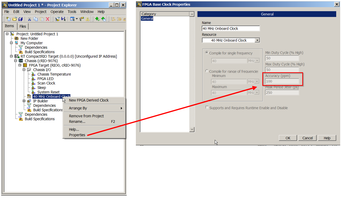
for each clock target (40 MHz on board and some derivatives clocks - if the target allows and you created them) you can find the accuracy of the information in the Project Explorer by right clicking on the desired clock and selecting Properties. See attached picture. What is the answer to your question?
B/R
Tags: NI Hardware
Similar Questions
-
Independent of the 40 MHz clock Onboard FPGA PPS GPS meter
Could you give me some advice or point me in the right direction?
I need to time counter accurate/tick synchronized by GPS PPS synchronization signal.
I got cRIO S.E.A. GPS Module that trigger PPS signal at the bottom of basket FPGA. PPS rising edge signal precisely mark the beginning of the second.
When I measure the number of ticks of 40 MHz clock FPGA embedded in a (PPS) second number of ticks is not 40.000.000 ticks but something like 39,999,800 ticks.
I want to measure with precision time between edges up/down digital signals. Because the clock of 40 MHz FPGA are drifting I can't use it.
How could set up my own witch counter ticks will be put away with signal GPS PPS?
I don't expect that I could provide 40 MHz FPGA on board the oscillator.
Should I create my own counter which will increase the opposite by the value 1.000,005 (40 000 000 / 39,999,800) each tick and this counter will be running timed loop (chronometric 40 MHz FPGA embedded base). Increment the value (1,000...) will be updated every seconds dependent PPS vs FPGA clock drift.
My configuration: cRIO-9025, cRIO-9116, S.E.A. GPS + cRIO module, high-speed DIs NI 9402, RT/FPGA LabVIEW 2011
Looking forward to your hearing you.
PeterHi all
This could help you.
Timekeeper FPGA
- http://digital.NI.com/public.nsf/allkb/EFDC35727D4F2CC086257A0700693003
- https://decibel.NI.com/content/projects/NI-TimeSync-FPGA-timekeeper
(I do not understand how this could be released on 23/05/2012)
-
Use of FIFO memory on two areas of clock (Labview FPGA) block
Greetings!
I'm developing an application on the FPGA of the vector signal OR 5644R
transmitter/receiver. I have two loops single-cycle timed: a 40 MHz making a convolution
and writing a FIFO memory block and the second at 120 MHz (sample clock)
who reads from block FIFO memory and uses the following values
interpolation...Under what circumstances is it permissible to use a FIFO memory block to transfer
values of a loop from 40 MHz to a loop of 120 MHz (sample clock)?
The reason I ask the question, it is that the compilation of my code repeatedly of not
reported the error below:ERROR: HDLCompiler:69 - "/ opt/apps/NIFPGA/jobs/J9k7Gwc_WXxzSVD/Interface.vhd" line 193:
is not declared. I share for everyone's reference, screenshots of my code which is an extension of
sample 'Project streaming VST' given in NI5644R. A brief description of attachments is
given below...
1. "Top_level_FPGA_part1_modification.png": in a loop SCTL 120 MHz, a sub - vi bed FPGA
go a block FIFO memory... In fact, the reading is actually made when entry
"read_stream" is activated... (see details in read_from_fifo_true_case.png)
2. "Top_level_FPGA_part2_modification.png": a 40 MHz SCTL, wherein is a subvi FPGA
called to write the output of convolution to block FIFO memory.
3. "target_respone_fpga_block_FIFO_modification.png": an output of a convolution filter is
written in block FIFO memory each time that the convolution output is available...
'ReadBlockFIFO' VI (circled in Top_level_FPGA_part1) is invoked in a 120 MHz SCTL.
4. "read_from_fifo_false_case.png": when the input "read_stream' of this vi is false,
data transfer memory FIFO of block to a different FIFO ('generation filter") takes
place.
5. "read_from_fifo_true_case.png": when the "read_stream' is set to true, the data is read in
'Filter generation' FIFO and spent on the chain of later interpolation to the
120 MHz SCTL...
I hope that the attachments give enough clarity to what I'm doing... If we need
For more information, do not hesitate to ask...
Kind regards
S. Raja Kumar
Greetings!
I think I understand the problem... The error probably occurs because a DMA FIFO
(FPGA host) is playing at 40 MHz, and it is checked for the number of items in a loop
120 MHz... It is not captured by the "pre-processing" by the labview FPGA, but by the Xilinx
compilation phase synthesis tool.
A lesson I share, is that if you observe this kind of problem, watch if there is incompatibility
in the areas of the clock to access a FIFO...
Kind regards
S. Raja Kumar
-
Embedded FPGA vi - network shared variable not updated
Hello
I work with an ethernet RIO 9149 of data acquisition. I use a hybrid programming mode.
I have a very simple FPGA VI that I downloaded on the flash memory. I used the indicator led to show my VI runs once the power of the RIO. Everything is fine, except that my shared network variables are not updated in the DSM ("no known values" displayed). However when I run the FPGA VI of my laptop, only once then stop and close (with 'interactive execution'), then my shared variables are updated in the DSM.
Any ideas why is this and how do I get the RIO update automatically shared variables without having to run the VI once?
Thank you very much.
Hello
I did a few tests and research and discovered that it doesn't seem to be possible. It is important to note the difference between Network-Published static (NSPV) and Variables of e/s of Network-Published.
The other are "user defined variable I/O" to communicate between FPGA and RT (RT absent on chassis Ethernet as the NI 9149) host. If these variables are checked to be published-network (in properties). They are accessible by VI running on the hosts of the same LabVIEW project, so you need to run a VI to access, as you mention. This is explained on the next page, Variable IO data custom FPGA of e/s (real-time Module or Module FPGA):
https://zone.NI.com/reference/en-XX/help/371361H-01/lvioscanhelp/io_vars/#user_IOV
I did find a way without a host (host RT or Windows PC) running a VI. If you have a cRIO with RT and NPSV host in the RT VI it is possible.
-
The export of clock FPGA embedded modules e/s
Hello
Is it possible to export the clock embedded FPGA, or derivatives, all Modules e/s?
Greeting
Matthias
I assume that this refers to one NOR 9225, 9227, module x 9229 or 923 in a CompactRIO chassis. You cannot export the clock aboard 40 MHz to these modules. One of the modules must be a master, and then you can sync the time base for all modules by setting the Source of the master time base in the Module C Series Properties dialog box.
Export the 40 MHz clock would not allows you to acquire data much faster still. Depending on the frequency of the time base, you can calculate using NI 9225 manual Instructions and specificationsdata rates. However, you are still limited to sampling frequencies in the specified data range. For a base from time to time as 12.8 MHz, maximum possible sampling frequency is approximately 51.2 kech. / s instead of the available 50 kech. / s with the time of 12.8 MHz base.
-
FPGA (PXI-7852R) Square Wave DIO
I need to improve the noise to the DIO square pulse pulse width. With my current code (attached .png) I see 25 ~ ns jitter on the front coming down from the impulse (I have the trigger on the rising) with my oscilliscope. This Jig is present even with only a single output square wave (i.e., I delete the other square wave generators).
Any ideas how to improve the fidelity of pulse width?
Thanks in advance!
25 ns is the period of your clock to 40 MHz, the jitter is unavoidable at this clock frequency. The DDS square wave algorithm produces a very precise frequency over time, but cannot control the speed at which it is called to update.
If you set the clock of the loop to a greater frequency of derived clock, you shoot the Jig by the same factor. Right-click on a 40 MHz clock embedded in the project with the FPGA target and choose new clock derived from FPGA. You may need to experiment a bit to see how high you can set the clock frequency without introducing sync in compiling violations; new targets will allow higher clock rates generally. Set up your single cycle timed loop to use the derived clock and don't forget to update your average square configuration with the new clock frequency.
-
Risk of static conditions of race FPGA
Hello
I'm fresh off a LabVIEW FPGA course and I feel have a decent understanding of him, but a co-worker on a project we start is push me for answers before I had the chance to 'play' with him.
The questions are:
1. How do you deal with racing conditions?
2. How do you deal with static hazards?
My first response was I think that LabVIEW "will be on it', that data-driven paradigm of"wire"will ensure that the race conditions occur, as long as I'm not using local variables or write to the same control/indicator, in which case I'll have to consider race conditions in the same way I old No LabVIEW FPGA. Static hazards, never heard mentioned in connection with LabVIEW, so once again I assume he took care of "behind the scenes"?
The application is the streaming of data to a NI-SMU-5644R and do some calculations embedded FPGA before streaming to the modulator if it has no effect.
Thank you
As long as you correctly follow the stream, you won't have a race condition. But it's something to be careful.
I don't never heard of static hazards being an issue with LabVIEW FPGA. One thing that does NOR is there buffers for each clock cycle. This will keep the static hazards away. Inside of a loop single-cycle timed, these pads are removed for all within a single cycle. I don't know what OR with these, but I've never heard of him being a problem.
-
Hello
I would like to create a FPGA loop that runs at a fixed rate. Whatever if I use a timed loop structure or a timer loop express VI into a regular while loop? Under what circumstances should I choose one over the other?
I understand that the timer loop approach can cause the code in the loop run twice before calendar is established (but this isn't a problem for me here). Are there other differences in the two approaches?
Thanks in advance.
JKSH wrote:
But my question was about the differences between the use of "multi-cycle" Timed loops and VI express loop timer.
In a targeted FPGA VI, all call loops are single cycle timed loops (SCTL). This means that all the code in a SCTL must run in a clock cycle, so there are a few types of nodes cannot be used in such a loop. In a used while loop with a timer, you can use a wider range of features, but the loop will generally run much more slowly.
These documents may be useful to learn how to use loops clocked on FPGA:
Using loops of Cycle time unique to optimize the FPGA VIs
Optimization of your screws of LabVIEW FPGA: running in parallel and Pipelining
-
Hi, I'm using LabWindows/CVI 2010 with NI Vision and NOR-IMAQ libraries and map of CL 1427.
I would like to know how the Vision Development Module handles the imaqSubtract and imaqThreshold functions, are they run to the hardware or software level? I wrote my own functions of subtraction using the address of the buffer for the image and the loops but you don't you 10 Hz compared to 30 Hz with imaqSubtract VDM functions. Thank you!
FeralPhys
Yes, they are handled in software on the host computer. The 1427 Camera Link adpater does not contain an FPGA, you can use for the treatment of the physical image. You can configure the driver to search for harware database (you can do this in Max and then save the file to the camera). But that's all. All features of Vision in CVI will run on the host computer.
If you are interested in processing equipment, the PCIe 1473R can do so by using its embedded FPGA, but you need LabVIEW FPGA to do programming.
It is more complex, but can be useful in critical applications at high speed.
-Christophe
-
Basis of LabVIEW Development with Compact RIO device software
Hello. Currently, I have the LabVIEW Base development software package and have been using it with DAQ Compact devices for the acquisition of basic data. I would now like to start integrating controls in my system, changing to RIO Compact for deterministic real-time features. My question is that I would be able to build applications for the Compact RIO system using only the basis of LabVIEW Development package without updating immediately? Maybe some features are not available for me, but could at least get a good start like that?
A CompactRIO embedded time real operating system (RTOS) called VxWorks you need to target the deployment of LabVIEW code to the device. Classic LabVIEW screws you will have been written so far are built to target general purpose operating systems (GPO) such as windows.
To create screws that are deployable to STSOp, you will need the real-time Module that is not included in the basis of LabVIEW. As a result, to take advantage of the embedded FPGA, you'll need to install the LabVIEW FPGA Module as well.
As long as you have the FPGA modules and in real time, it seems to me that you should be able to control these devices with LabVIEW Base. Without these software components you will not be able to create an instance of the device target your LabVIEW project.
-
generate signalexpress of digital output or 6009
Hello
I'm a user of Labview SignalExpress rokkie. I would like to generate outputs digital, but when I try with N samples or samples continious it does not work, it gives the error which is
Error-200077 occurred to the DAQ Assistant
Possible reasons:
Measurements: Requested value is not supported for this property value.
Property: SampTimingType
You asked: Sample clock
You select: On-demandAlthough I can generate a sample so could you please help me on this problem?
Kind regards
ERS
As mentioned previously, the USB-6009 case supports the outputs digital NI. "N samples" and "Continuous" generation modes are available only for devices that are able to use a clock embedded to generate samples. Input analog on USB-6009 uses can use an on-board clock and can thus use modes "Continuous" and "N samples. The better you will be able to do with the USB-6009 case is to switch the value on and with a timing of software. A solution would be to use a step DAQmx Generate to set the high value, a stage of execution to allow reuse of the material, and then an another DAQmx generate step to set the bass line. Run this in a loop and you'll get something of a digital pulse train (although it is not terribly pretty.) It will be quite slow and very non-deterministic. This means that some iterations may take only a few milliseconds, while others may take much longer.
Kind regards
-
Encoder triggered Acquisition (Single Channel N samples)
Hello Internets,
I am an inexperienced user of LabVIEW, I'm trying to set up a system in which blood samples are taken when triggered by a digital pulse.
I'm sampling using a PCI-6250. I have an updated encoder in place that emits a digital pulse once per turn. I would possibly take about 1000 samples in a very short time triggered by this time by pulse rev.
The problem I have right now is that I seem to get a lot less reading I expect otherwise, the LabVIEW program, I'm running also takes a long time to stop following my pressing the stop button.
The table fills also in a way that is strange to me, perhaps someone could it explain?
Thanks, any help would be greatly appreciated!

Hi Relaxidermist,
There are a few things in your current code that seems contrary to your goal:
"I would possibly take about 1000 samples in a very short time triggered by this time by pulse rev."
Assuming that you want to read 1000 samples for each received external trigger and you have several triggers coming, I would start by this example:
Redeclenchables analog input finished using digital triggering
I'll be the first to admit that he is not the most intuitive - on the M-series (like your 6250), use a meter to output to an acquisition really triggered. You could rearm task in the software, but this takes time and is prone to triggering signals are missing.
If you were on a series of X (63xx devices), the code you have is close, but you must make the following changes:
(1) use the clock embedded to your example of clock instead of the external signal for PPR source.
(2) make the task finished instead of continuous.
(3) enable the redeclenchables property - it is not available on your device of the M series (where workaround posted above).
Best regards
-
specifications of clock sbRIO-9651 SoM FPGA fabric.
Hello
I would like to know the following specifications about the clock (clock of fabric) FPGA of the NOR sbRIO-9651 SoM:
-Precision (ppm)
-Aging (ppm/year)
-Temperature (ppm / ° C)
-Skew (ppm)I couldn't find anything related to this in the specification document.
Is it possible to use an external clock to repalce this one if the specification does not meet our requirement? This clock would be managed by a Board of business custom.
Thank you
Michel
Michel,
The accuracy of the clock is ±50 ppm. You can use an external clock as a source for single-cycle timed loops. The first logical level - things outside SCTLs - is still controlled by the internal oscillator at 50 ppm, but logically or e/s who needs a different precision can be placed in a SCTL and use the external clock. There is some good information on how to import a clock on our developer community material for NI Single-Board RIO and module system. Remember that the quantity of resources used and their frequency toggle will have an impact on the overall jitter of your system.
Thank you
Bryan
-
Clocks on board and derivatives of FPGA
Hello
I use a PCIe FPGA 7852R card to collect data at 200 kHz of channel 5. I was pretty confident that my collection frequency was correct, because my program was based on a derived clock of 40 MHz I had chosen to use a derived clock because the on-board clock is running at 40,02 MHz (instead of the 40 MHz specified for some unknown reason I ignored).
However, today one of the members of the LabVIEW support team told me that the FPGA clock rate may change during the compilation and optimization (constraints). He stressed that if the FPGA can run that fast, then it displays an error (as you might expect). He said also that in some cases, the on-board clock can run faster, but in this case no error will be displayed. I saw no errors in the past (which means that the system had no problem with that fast running), however, I'm not sure if during one of my compilations my derived clock could have run faster than 40 MHz. If it can happen? This will affect the time of all of my previously acquired data. Unfortunately, I have not saved any of my journal compilation of
 .
.Thank you very much in advance.
Kind regards
Varun
Hi VarunSreenivasan,
I think that our support has meant that compile logs will show you some pieces of logic could operate at higher speeds. During the process of compilation, the compiler will determine the clock frequency more rapid that can be used for your logic and to ensure that the configured clock frequency is less than or equal to this value. If you have decided to try to run your code to 200 MHz and logic cannot run this fast, then you get an error. If you have decided to run your logic to 200 kHz and it is possible to run faster compilation logs will show you then the max frequency that will work, but the logic still run to 200 kHz. The code should run no faster than the frequency you specified.
-
How to increase data FPGA clock?
I use LV 14 and 14.5 USRP. When I plug my new USRP-2940R-120 and run a program written for a USRP-2940R-40, the driver gives me a message that says "you are using a bitfile configured for data clock which is slower than the rate required for the bandwidth of this device. Risk of aliasing in your signal. "(error 1073383043).
Fair enough.
Then I looked at the data of properties of the clock in the application project and that I could not change the values in there. Then... How can I change the data FPGA clock frequency and what do I change to?
Thank you.
Hi emonk,
We have created a new FPGA target what samples at 200 MECH. / s to use the increased BW. You need to recompile your application using the new target. My recommendation on the best way to proceed is as follows:
1 generate a new project of the sample. With NEITHER-USRP 14.5 all the projects in the sample have now both targets (120 MPS and 200 projects of average size)
2. don't customize you the FPGA in your application? What if not all you have to do is use the bitfile for the target of 200 MECH. / s of the project in your host code example. If you did, you will have to redo these customizations in the FPGA VI of high level of the target. It can be trival or difficult depending on your application,.
3. you will then need to recompile. Because of the faster clock rate, the meeting schedule is more difficult, your FPGA IP may need to be optimized if you work in the field of data clock. I suggest that the kickoff from 5-10 compile at first because of the variabiliy in each compilation. If all still fails, use the timing to study reports where optimizations are needed.
I would like to know if you have any questions or encounter any problems.
Maybe you are looking for
-
Account restriction - Contacts App
Hello everyone, I have an iPhone 6 + and I'm trying to block it so my son can not add contacts to his phone. I went to and set restrictions on the phone to prevent changes on account settings since he says includes contacts, but I can still add. Am
-
Satellite Pro L100 CPU upgrade
Hello The hope for some advice. I recently bought a Satellite Pro L100 of second hand, came up with the following configuration. Celeron M 370, 256 MB Ram, 40 GB drive HARD, Win XP As the laptop is out of warranty, I disassembled the laptop and upgra
-
How to stop startup programs unnecessary popingup when I start my pc
How to stop startup programs unnecessary upward poping when I start my pc
-
I can't in internet explore unless I have restore my system before 14 Oct automatic updates - daily
-
will XP backup includes the files in the backup folder (software) system?
Hello. I installed a software, which then itself has improved in a new version. If I use the XP Backup utility, will be that the saved file includes all of the files in this software, including system files, thank you