4110 parallel PXI 2 outputs isolated
Hello
I'll use 4110 PXI to provide HAD. If HAD current exceeds 1A, is there a risk to 2 isolated parallel output to provide more current? Y at - he notes that I have to take?
Thank you
Leo
Hi Leo,
On the 4110 you can link channels 0 and 1, but unfortunately you can not link channels 1 and 2 because they share a floating ground and channel 2 is negative only. Theoretically, you could bind the channels 0 and 2 together, which would be useful if you need then a more positive than this handset rail voltage. Note that channel 0 is only 0 - 6V, so you will need to limit the voltage set to this output range.
Tags: NI Products
Similar Questions
-
I am trying to simulate a radiation of 3 mV/V power pressure transducers (excitement is + 10V, full range should therefore be 0mV at 30mV). I am looking for a PXI analog output device high number of channels (PXI-6723, possibly) who doesn't have the down side of the analog output channels linked to the land of installation (differential channels of AO). The plan was to use a voltage across the divider circuit of +/-10V output card AO to +/-50mV. I use a card AO 16-channel, 12-bit which has all the Commons AO related to the mass of the PXI chassis and Earth installation. The DC of the signal part I want it, but there are about 80-100mVpp of noise (from the ground connection) riding on it. I also tried a PXI-6115 card we had at hand and its reference AO are related hard chassis-same result with the noise of the Earth. Is PXI - 6723 AO GND isolated from the land of the chassis/installation? Even if all GNDs AO are shared on the Board, this solution should be much better than having a noisy ground reference.
Any ideas? Alternatives to simulate a floating, the millivolt output device?
Thank you!
The reference of the AO of the 6723 relates to Earth; pages exit track to track analog insulation research, only a handful of AO devices have an isolated field (the business is a low channel count).
-Ciao
-
PXI-6704, parallel to the measurement of the resistance
Hello
I'm in show two separate circuit analysis procedures. First of all I would like to provide two pins with current and measure the response of circuit elsewhere, and second, I want to test the total resistance not fueled between those two pins. If I have a current PXI-6704 output wired to the pair of pins and the value 0 output amp, it will interfere with the measure of resistance to these pins (as a parallel resistance) or if it excludes all signals and appear as an open circuit?
I can use the PXI switch to connect and disconnect the DMM to measure, but test specifications require no supply current through the switch.
I don't have the equipment to hand, I know it would be the fastest test. We design the test set-up circuit in parallel with the PXI test chassis.
Thank you
Mello
Hey Mello,
Thus, the output impedance of your card is 1GOhm, so unless what you measure is huge, so it should appear as an open circuit. I hope this helps!
-
Large signal output capacitance measurements
Hi all
I'm working on a power amplifier and I want to measure the ability to output under large signal condition. I use a non-linear model of the GaN power transistor.
Power output is about 36 dBm, f = 8.2 GHz
I tried both methods:
(1) I have spent under bias Vgs - 6V to 1V, Vds = 28V. I use solver C_PRC linear tab to find the parallel to the output capacity. I got a chart that changes from 0.3pF to 0.5pF. In this simulation I don't use tuner to impedance, just ports (50 ohm) and sources of bias.
(2) amplifier is biased to 28V and 125mA. Then, I drive amplifier with of 20dBm to 30dBm input power. In this simulation, I used HBTUNERs to maximum power output (power input 25dBm at the entrance) and the output. I can see there is a change in capacity at the entrance vs input power change. However, in the output, production capacity is constant and 0.52pF. I am able the ability of the drain of transistors, tuner. I use great Solver for the parameter measuring signal Y and calculate the capacity.The interesting thing, I can meause entry changes easly to large signal capacity, but output capacity is constant!
I have two questions:(1) why the three measures are different?
(2) for large signal measurements, for example; 30dBm output, 30 v peak-to-peak output average 40dBm 50 v peak-to-peak. So, there is a change in capacity over a period of time. When I measure the Solver big signal, Solver uses the high peak values? If so, can I change low peak value?
(3) can be used for important signals gamma probes?
Thank you
-
Why voltage does not change when I put a resistor in parallel?
Hi all
I have observed something that seems quite strange and I do not understand. I'm under Multisim 10.1.1.
I have a sinusoidal voltage source that is diode full-wave rectified by a RC parallel network for the purpose of obtaining 120VDC, who has everything works beautifully. I am in a position the voltage with a voltmeter. Crazy is when I put a resistor in parallel with this output 120VDC, voltage drastically changes. For example, when I put a resistance of 1kohm in parallel with the release of 120VDC, the voltmeter reading falls drastically to 0.835V.
Of course if I perform this test with a simple DC 120V source, the voltmeter reading remains stable at 120VDC.
Does anyone have AN idea why this is happening? I am full of ideas. Thanks a lot for all the help in advance!
Sorry for the frequent posts, I was not thinking clearly yesterday night when I posted this question. Voltage divider simple problem. Sorry again!
-
FPGA interface of data acquisition
I have a repetitive loop in a PXI-7813R producing reasons. The output of the PXI-7813R is TTL, but I need 0-15V levels. In the same PXI chassis, I have a DAQ (PXI-6528) hardware that can handle the voltage levels. The question is, can I somehow link the the 6528 7813R patterns using PXI backplane and leave this market while I wear the use of PXI rack for other functions?
Thank you
Andy Quick
The problem with the PXI-6528, is that it is software programmed. Which means trigger won't help you here.
What you need to do is to do some work of material. You can have the PXI-7813R output profiles and drive an opto-coupler or FET circuit to change the level of voltage of 15V. Or maybe there is there a digital stamp which can output 15V for you.
-
How to break a digital input continues to arduino into pieces
Hello
Basically I have a shift register parallel-input series output connected to an arduino UNO, which is interfaced with labview. The exit of shift register is fed into pin Digital arduino with eight inputs 1 or 8-0. what I'm trying to do is to assign each bit of the digital pin of the arduino to a LED on the front panel in labview. For example, if there are four 1 and 0 to read the arduino pin ovens then four of the conduit must be on and four must be turned off. Any help would be grately appreciated.
Thanks in advance.
You already have the table Boolean number. This is the part I was worried to find you. Table of Index to get the Boolean individual out of the picture. And Index table is expandable, you only call him once in this case. Expand it just to have 8 items and wire up your LEDs.
-
PXI-4110 deactivation and activation of the output
I'm programmming power CC PXI-4110. I want to activate and deactivate the outputs. I use niDCPower_Disable() to disable the outputs. and the use of niDCPower_Initiate() to activate the outputs. Problem is after I have activate the outputs with niDCPower_Disable() and with niDCPower_Initiate() that I lose all my settings as the output voltage. What I so niDCPower_ConfigureVoltageLevel() and niDCPower_ConfigureCurrentLimit() call before calling niDCPower_Initiate() then outputs are put to the required voltage.
I want to do is turn on and off just like pushing a button on a Panel.
For example, I call niDCPower_Disable() to open the relay switch.
It seems to me like there is a function niDCPower_Enable() which would close this switching relay and not reset all my voltage and current limit settings.
Any help on the best way to proceed would be appreciated.
Figured it out using:
status = niDCPower_ConfigureOutputEnabled (vi_4110_0, channel0Name, VI_FALSE);
to turn off and then I start with
status = niDCPower_Initiate (vi_4110_0);
In this way, my diet is ready to go, but my relay is open.
When I'm ready to close the relay I follow these steps:
status = niDCPower_ConfigureOutputEnabled (vi_4110_0, channel0Name, VI_TRUE);Then later I want to open the relay call again I have only this:
status = niDCPower_ConfigureOutputEnabled (vi_4110_0, channel0Name, VI_FALSE);
Problem solved.
-
OR DC Soft Front Panel, minorbug, small bug with the PXI-4110
Hello
The NI DC Soft Front Panel V14.0, with the PXI-4110, scrolling to negative tension, works as expected to-10V, but then returns to 0. If we change from - 1V procedure, it goes...-8-9,-10, -1, -2... instead of-8-9,-10, -11, -12...
Everything about her, a simple thing that I miss is a switch for all three voltages.
(Also, IMO, it would be logical for negative tensions with the arrow pointing down, not more).
My 2 c
Hello Janaf,
I completely agree with two of your statements, I tabled a report of corrective measures that you can monitor in the next versions of DCPower to see if this is fixed with the FPS. CAR number: 512257
I've added notes that only manual insertion of numbers - less than 10 works and that it was not logical to use arrow increment or upward arrow to reduce the output voltage.
-
Sequencing of power through individual PXI-4110
Hi all
I have a hardware device that requires a sequence of power-up/power-down very specific in order to work properly and not be damaged. According to the data sheet for the PXI-4110, he is able to meet the requirements of power, but I use Labview to create a VI of sequencing of power for each channel.
After investigating the options and study the DCPower examples, I understand how to set each channel, but from what I've seen, real initialization (property Initiate.vi) will supply based on "the instrument handle" alone, rather than undertake each channel of the instrument individually.
Is there a method to use Labview screws to separate the different channels of the PXI-4110 and control the boot sequence for each channel?
Thanks for your time.
Kind regards
GSinMN
Hey GSinMN,
Yes, you would be able to run a loop to increment the output in stages, but of course, the more steps, you have as much time as it takes to achieve your final value. My concern would be that you go time 200 ms if you had too many steps. Also, your total rise time will vary depending on your CPU, as well as other processes run you in the background.
If you compared the rise time on a certain CPU with some process running, probably not having the same rise time when porting your code to another machine.
It may be useful to ask the manufacturer of laser if they have no indication of what the tour of ramp at the time should look like. The 4110 is designed to have a fast rise time with minimal excess for most of the charges, but it would be good to understand what they need for their laser. Maybe is it acceptable to have a fast rise time, as long as the output does not exceed x % of the final value? Any idea that they have on this would be helpful.
Please let us know how we can help.
Thank you!
Brandon G
-
Current limit for the PXI-4110
I'm a PXI-4110 with LabWindows programming. I'm trying the current limit. I have an output to 5V with a load resistance of 1 K; This makes the current 5mA. I put the current limit of 2mA to work. When I read the voltage and current is 5V 5mA. Here is my code:
g_voltageLevel_ch0 = 5.0;
g_currenLimit_ch0 = 2.0E - 3;
status = niDCPower_ConfigureOutputFunction (vi_4110_0, channel0Name, NIDCPOWER_VAL_DC_VOLTAGE);
niDCPower_error_message (vi_4110_0, status, errorMessage);
status = niDCPower_ConfigureSense (vi_4110_0, channel0Name, NIDCPOWER_VAL_LOCAL);
niDCPower_error_message (vi_4110_0, status, errorMessage);status = niDCPower_ConfigureVoltageLevel (vi_4110_0, channel0Name, g_voltageLevel_ch0);
niDCPower_error_message (vi_4110_0, status, errorMessage);
status = niDCPower_ConfigureCurrentLimit (vi_4110_0, channel0Name, NIDCPOWER_VAL_CURRENT_REGULATE, g_currenLimit_ch0);
niDCPower_error_message (vi_4110_0, status, errorMessage);I find that if I put my current limit to channel 0 to 10mA, above the error message disappears. However, I can put the current limit for channels 1 and 2 to 2mA, and I do not have an error message with them. I see nothing in the power supply on a valid range on the current limit. To be clear on what happens if I do this:
status = niDCPower_ConfigureCurrentLimit (vi_4110_0, channel0Name, NIDCPOWER_VAL_CURRENT_REGULATE, 8-3);
I get the error "Invalid value for the parameter or property."
However, if I do this:
status = niDCPower_ConfigureCurrentLimit (vi_4110_0, channel0Name, NIDCPOWER_VAL_CURRENT_REGULATE, 10th-3);
I don't get an error.
Channels 1 and 2 do not have this limit. I went down to 1mA on these channels and no problems.
-
Calculation of the frequency of real output of a PXI-5402
I have a card PXI-5402, sitting in a high chassis. I'm only interested in the sine wave output at frequencies up to about 10 kHz. I know that it is possible to request an output frequency and then interrogate the acutal output frequency but I prefer to be able to calculate before hand. All I can find in the literature is a figure of 0.355uHz for the frequency resolution.
Is there a better description of the frequency resolution? If this is not the case, the resolution is exactly 0.355uHz or is it an approximation (to 3 significant digits)?
This webcast is a great way to learn the process including the NI 5402 5406 OR exploit to generate periodic duty: http://www.ni.com/webcast/75/en/
The 0.355uHz value is a theoretical value of the frequency rate achievable depending on the size of the accumulator Phase and clock frequency. It's the closest thing I can find on ni.com that you can use to calculate the value: http://zone.ni.com/reference/en-XX/help/370524R-01/siggenhelp/ni_5401_11_31_frequency_resolution_and...
According to me, Fc for the NI 5402/5406 must be 100M and the size of the accumulator is 48 bits. Frequency resolution so = Fc / 2N = (100 × 10 ^ 6) / 2 ^ 48 = 3.55271368e - 7
Keep in mind that the device has a VCXO frequency accuracy specification of + / 25ppm, if you have no PLL block him to a better source.
-
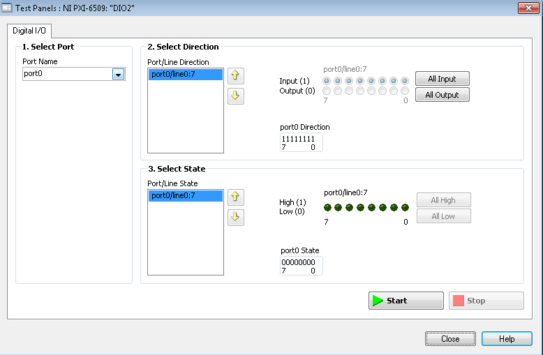
Individual access to the inputs and outputs on a single port (PXI-6509
Hello
I use PXI-6509 and this sentence taken from the Manual:
"You can use each of the DIO lines as the input to a digital static (DI) or digital output (DO) line"
leads me to believe that each individual DIO can be defined as input or output (even within ports), but picture:
shows that these ports can be defined as inputs and outputs in the same port.
On another card 6284 with DIO, I can put them individually.
Can someone confirm that the 6509 is correctly?
Best regards
Adrian
-
PXI-6133 Pulse frequency output and input with DAQmx
I am trying to set a pulse meter output frequency task and read this signal with a frequency counter input task input pulses. I use a 2 PXI-6133, each connected to a BNC-2090 case has. I want to output a square of a certain frequency with the task frequency meter pulse output and then read the frequency of this signal using a task of cost input frequency. I don't know how to property set up these tasks, or how to define which device to use for each heap. I don't know what terminals on the BNC-2090 is the counter of entry/sortient channels correspond to them because that is not displayed in the documentation of the PXI-6133 or documentation of BNC-2090.
Please see the attached VI for my attempt to put this in place. Currently, I get two errors:
(1) error-200452 took place at the property Node DAQmx channel meter Test - referred to as property is not supported by the device or is not applicable to the task.
2. the error-89136 at DAQmx Start Task - specified route cannot be met because the hardware does not support.
If I remove two channels of property DAQmx where I try to put the terminals for the counters, while the program is running, but then I know not what terminals on the BNC-2090 meters are connected to! This causes the DAQmx read for the cost in the tasks of frequency to timeout because it does not detect a signal.
I would really appreciate the help to properly configure these tasks and determine what terminals on the BNC-2090 case has the task of counter will work on.
I see a few problems in the code originally:
- For your CI task, you type is defined as a counter entry > frequency. But on the node property of DAQmx channel for this task, you modify the CI. Property of PulseWidth.Term. It should be CI. Freq.Term. set the entry regardless of the PFI line you do not want the input signal on. Tip: you don't have to type the name of the device in at all. Enter "PFI0", it's the same as "DevN/PFI0" since the unit has already been specified in the DAQmx Virtual Channel Create function. The name of the device, leaving aside will make your code more flexible where you decide later to change the name of the device.
- Maps of the S series, such as the 6133, do not have the same flexibility to change the output terminals of tasks of meter you might find with M or X series device. Page 83 of the S series manual watch what signals can be extracted to PFI lines - Ctr0Out is not one of these. Instead, Ctr0 out is, by default, pin 2. Cabling to a BNC-2090 6133 is certainly difficult to understand out (probably because the 2090 was designed to work with the materials of the E and M series), but if you compare the pinout of a PXI-6255 0 with the 6133 pinout connector, you will notice that they are essentially a match 1-1. Pin 2 is PFI12 on the 6255, so I assume the same for the 6133. All this to say, Ctr0Out always appears on the pin 2/PFI12 for the 6133 and you therefore cannot change the output terminal that your code is trying to do, having for result error-89136. Remove this node from the property altogether and the error should disappear.
-
What is CH 0 output power awg PXI - 5422?
I would like to know what is the minimum and maximum of the CH 0 terminal power in my AWG. It is inserted in a PXI - 1031 dc chassis. I looked through the sheet attached PXI - 5422 and page 10, it lists some tension, the configuration of the amplifier and the dBm output power. For example, Low Gain--> Vpp--> dBm 4.0 1.00 seems to be a unit of energy conversion because putting Vpp 1.00 through the equation of power gives Pout = 10 * log(V^2/R*1000) = 10 * log([(1.00/(sqrt(2)*2)]^2/50*1000) = 4,0 dBm written on the technical data sheet
 . In my equation, I took the peak voltage in crete, divided by 2 to get the voltage Amplitude divided by sqrt (2) to convert it to RMS and then used the power = voltage ^ equation 2/resistance and finally the Watts to the conversion of dBm. I guess as a 50 ohm load for which is what my AWG is currently set to.
If my analysis is correct, this implies the PXI - 5422 has AWG of a range of output of-20, 50 dB (0,00891 Watts) up to 25.6 dBm (363 mW). The problem is that the 2 I work with scientists say it's too much power, because the output power of the GTS should be able to be directly connected to the digitizer we (NI PXI-5761) and turn off the 25.6dBm will definitely FRY. According to them, a range of 0-10 dBm is more reasonable than the power output CH0 AWG.
My analysis is correct? Further reflection?
Thanks for the research!
Hello
It's Marcus of Engineering Application at National Instruments. I've reviewed over your math and you are correct in your calculations. To determine the power output of your PXI-5422, you will need to know the Vpps that you use and also the load to which you connect to the device. These factors will then determine the power output of your PXI-5422.
Kind regards
Marcus
Maybe you are looking for
-
I forgot my ipad apply id and now I can have access to all the
-
NB550D boots in black of the screen and cannot turn off even
I had my NB550D for only less than a month. I've updated the memory to 2 GB and the Op to Home Premium system, but nothing else. It's on auto update on security issues, and I remained with the McAfee protection which was pre-installed (and paid for a
-
Cannot restore the backup to iCloud. Stuck on "remaining time: estimate.
I bought an iPhone 6s a month ago. Saturday, the screen is dead - they said it was a bad card, so they gave me a new. Initially, the restoration of iCloud seemed to work very well, but some of my app data has not loaded up. These data are really impo
-
Loud fan after changing the hard drive
The hard drive on my IMac started 27 '' 2010 decisions feared chatter noise and slowing all work to a snails pace. By coincidence, a duff of my office iMac has exactly the same model number and size of disk (Hitachi 2 GB) so I switched them. The mac
-
Keyboard HP ProBook 4740 S moving area
Can you please tell me your opinion: is this normal or a problem? My thought is that the heat something was wrong in this area. Thank you! https://www.dropbox.com/s/z4m1pgztrxm7eqz/2013-04-22%2008.38.22.MP4 https://www.dropbox.com/s/0f7j0lb19lpqlbr/2