Advantages of RT on FPGA
Hi all
I used cRIO-9024 and cRIO 9113 in my latest project. Any control system was in FPGA. The host is responsible for doing some mathematical calculations (cycle counting, last race, etc.), display of the values of sensor (displacement, force) and control of some not so risky situations.
The first test was to communicate host RT with FPGA and then communicate host RT to the host via ethernet PC (i.e., I used a shared variable topology.). The first method was unnecessary because there were 120 shared variables. It was a lot slower that communicate directly with FPGA host PC. I then communicated with FPGA host directly by ethernet PC. It was the second method and it still works without any problem.
In any case, I really wonder the benefits of the first method in the second method, that I did. Should I really RT if all critical actions (control system) and all calculations are made in FPGA? If so, what is the reason?
I like the features of the C Series modules, so I will continue to use the cRIO platform but I think that there is something that miss me about RT
Best regards
Emre
It seems that you do not miss anything, it's just a matter of what is appropriate for your application. Some applications, such as yours, do not have an RT element. Other applications require a. For example, if you have a control and monitoring of the applications where the cRIO isn't always in contact with a host, a RT application can open values to a file that is checked periodically. An RT application can provide a network interface more flexible than a direct connection for the FPGA, such as a server that accepts multiple connections of clients written in different programming environments. In a recent project, I used a cRIO to control an ink jet printer. The application of the RT has agreed a bitmap over TCP, stored in memory and transferred on a channel DMA on the FPGA, which then triggers head inkjet synchronized to an encoder of entry. The main application is written in c# by other developers. The application of updated RT implemented a set of agreed order TCP so it acted as a stand-alone unit, and other developers didn't need to know everything about the implementation of the FPGA.
Tags: NI Software
Similar Questions
-
value whole County angle encoder
Hello
I try to trace the pressure exerted by a cylinder of an engine vs the rolling angle. And for each engine cycle.
I want to trace the value of the pressure of each degree which mean I value 720 by cycle because a cycle mototor corresponding rotation two of the rolling.
(I join a graph that represents what I draw simplify the 'pressure vs CAD')
My problem:
I have a quadratic encoder 3600 ppr which mean an accuracy of 0.1 °, but I'm just interresting to the total value of the angle.
So I traced the pressure value only if it is an integer, apparently, I miss a lot of them that's why I have a graph with 6 cycles instead of one.
(see attached "my results")
I think it's because of a timing problem with my curls on FPGA or RT or two of them...
I am open for every advice, examples or anything else that can help me
Best regards
Simon
I think you want something like that on the FPGA. You have to put your data in the buffer. See if you can understand the RT code to work with it. Basically, you want to read from the FIFO. Your problem is now that you are reading a control, which means that you can only read as fast as the RT can go. You lose the advantage of speed of FPGAs. Your FPGA should read point at a high rate. Your RT then reads multipoint pieces that are buffered to the top the FPGA. My suggestion is to read FIFO 3600 items at once (a full turn) on the side of the RT. Of course, it depends on how fast the encoder is rotating. I suggest you determine the maximum SPEED of your system will work on, and then set up your size of buffer accordingly.
I did the FPGA, but I wouldn't quite call me an expert yet. Others may come along with better ideas, but this is generally what I would do. WARNING: I have no test or check this work so it can certainly be bugs. Also, he is still waiting for the impulse of Z. In your application, you can wait the Z pulse once, get the TDC offset, then just stay in the inner loop. I didn't know whether you need synchronization with the Z pulse each time. Whatever it is, this should give you the general idea.
Edit: Have not yet had my coffee. I should only be to increment the account in the inner loop when I get a rising edge. And then I should be add to the FIFO only when the offset is greater than the offset TDC. Sorry, this mistake will cost you 20 minutes at compile time! I'm sure glad that I put this disclaimer clause


-
Basis of LabVIEW Development with Compact RIO device software
Hello. Currently, I have the LabVIEW Base development software package and have been using it with DAQ Compact devices for the acquisition of basic data. I would now like to start integrating controls in my system, changing to RIO Compact for deterministic real-time features. My question is that I would be able to build applications for the Compact RIO system using only the basis of LabVIEW Development package without updating immediately? Maybe some features are not available for me, but could at least get a good start like that?
A CompactRIO embedded time real operating system (RTOS) called VxWorks you need to target the deployment of LabVIEW code to the device. Classic LabVIEW screws you will have been written so far are built to target general purpose operating systems (GPO) such as windows.
To create screws that are deployable to STSOp, you will need the real-time Module that is not included in the basis of LabVIEW. As a result, to take advantage of the embedded FPGA, you'll need to install the LabVIEW FPGA Module as well.
As long as you have the FPGA modules and in real time, it seems to me that you should be able to control these devices with LabVIEW Base. Without these software components you will not be able to create an instance of the device target your LabVIEW project.
-
Hi all
Please, for the love of God can someone take a look at the attached FPGA project, I hit to the top and tell my why it is that whenever I run, as soon as he's trying to read/write on the host computer, it returns error-61046? A screenshot of the error is included in the attached .zip file.
I made many programs FPGA before with no problems, while using the same FPGA and FlexRIO module and never had this problem. If I run an example program it works fine so I am confident, that the error lies in my programming, I can just see where!
As you can see all the clocks are internal and appear to be configured correctly according to the example programs and other programs FPGA, that I have done before, so I'm puzzled. I hope that it is just my stupidity and lack of coffee.
Congratulations in advance.
Mitch
The pilot FlexRIO comes two CLIPs for the 5781. At ' a "NI 5781 Sychronous system" OR 5781 "VIDEO CLIP.
The "NEITHER 5781' is what originally delivered with the FAM and is always delivered with the driver for legacy purposes. I would discourage the use of this CLIP because it uses regional clocks for IO Module clock 0/1 which limit the amount of fabric that can be driven by these clocks to the fabric available in the respective region of the FPGA. The advantage of this CLIP, it's that the ADC and DAC can be clocked at different rates through a clock divider that exposes the CLIP.
The 'NI 5781 Sychronous system"CLIP is what is recommended for all new models. It uses a world clock which can target tissue in all regions of the FPGA. This CLIP uses the same clock to drive the ADC and DAC (IO Module clock 0). IO Module clock 1 is not used in this CLIP.
If you used the sychronous CLIP system and always a logic had driven out by IO Module clock 1 it that would explain why you received the error of non-response from IO Module clock 1 is left connected in the sychornous CLIP system.
-
Question of FPGA compile farm 2012
I was under the impression that my FPGA LV code can be compiled by several workers when I bought and installed the FPGA compile farm Toolkit. What I have, however, is that each work of compilation can only be compiled by a worker. I expect that a single compilation work can be divided by the number of workers.
So I see that a worker of computers will compile two computers of worker work. It's just that a worker will be compiled at the same time.
I just misunderstand the features to compile farm Toolkit or is it an installation problem?
Thank you
No, a unique compilation cannot be shared between workers. Nature of the beast-FPGA "compilation" is not something that lends itself to parallelism. You have the advantage that the build tools run much faster under linux, however.
-
How to choose the maximum number of items for DMA FIFO to the R series FPGA
Greetings!
I'm working on a project with card PCIe-7842R-R series FPGA of NOR. I use to achieve the fast data transfer target-to-host DMA FIFO. And to minimize overhead costs, I would make the size of the FIFO as large as possible. According to the manual, 7842R a 1728 KB (216KO) integrated block of RAM, 108 000 I16 FIFOs items available in theory (1 728 000 / 16). However the FPGA had compilation error when I asked this amount of items. I checked the manual and searched online but could not find the reason. Can someone please explain? And in general, what is the maximum size of the FIFO given the size of the block of RAM?
Thank you!
Hey iron_curtain,
You are right that the movement of large blocks of data can lead to a more efficient use of the bus, but it certainly isn't the most important factor here. Assuming of course that the FIFO on the FPGA is large enough to avoid overflowing, I expect the dominant factor to the size of reading on the host. In general, larger and reads as follows on the host drive to improve throughput, up to the speed of the bus. This is because as FIFO. Read is a relatively expensive operation software, so it is advantageous to fewer calls for the same amount of data.
Note that your call to the FIFO. Read the largest host buffer should be. Depending on your application, you may be several times larger than the size of reading. You can set the size of the buffer with the FIFO. Configure the node.
http://zone.NI.com/reference/en-XX/help/371599H-01/lvfpgaconcepts/fpga_dma_how_it_works/ explains the different buffers involved. It is important to note that the DMA engine moves data asynchronously read/write on the host nodes and FPGAs.
Let me know if you have any questions about all of this.
Sebastian
-
I use a NI7962R FlexRIO, with (for the most part) stock CLIP Socket NI6587. I have a compilation respondent timing probably 2/3 of the tent that I do. The synchronization will fail in the field of pin 125 MHz. Last night I re ran a compilation had changed nothing on the block diagram, and the tools were able to close the timer in BY. When it fails, ~0.5ns is missing, and it goes through more than 0.9ns when I have a successful compilation.
I have records (nodes of feedback) about every single control/led/DMA-FIFO, and the block diagram has been reviewed by an AESpecialist to find and take advantage of the design possibilities for the closing of the calendar.
Is it possible to get labview FPGA to allow smartxplorer shotgun approach to implementation?
-J
Hi JJMontante,
It is not possible to use SmartXplorer with LabVIEW FPGA Dev environment.
While it is annoying, I can offer a simple recommendation for you however. If you have a license for the FPGA compile farm, you can create several specifications of generation that point to the same high level design. This would allow you to spawn several compilations to your farm at the same time... always allows you to realize a shotgun approach. Many of our internal development teams use this approach on very tight compilations. If you have any other questions on the subject, I'm sure that EI specialist that you worked with you can contact me if necessary.
-
Error: Execution of registry is supported only on the FPGA target
I am trying to write a debugging tool to test the communication between objects FP on my host VI to a RT system and then to a FPGA system. I thought I would "simulate" the three layers with queues between them in order to ensure that the parameters are received correctly - a comprehensive test of Communications virtually. I want to be able to run this VI on the host. There are a lot of bits being shifted and twisted and be able to define probes and braekpoints within a single host VI is an advantage.
Initially, it worked fine after copying my FPGA code (with object instantiation of the registers and then reading and writing for them), but now then LabVIEW did another thing that disappears (with no goodbye or anything like that). When I say that it worked, the values read from the FPGA objects that instantiate their own records showed the correct values when sending data. This means that LV really instantiate records and has been able to address them individually.
Since then, I get the error appearing in the title, whenever I try to run the VI.
(1) should I really move my parts FPGA to a VI on the FPGA target and have the VI in parallel with the defined target to run in Dev mode (and sends data over the DMA channel)
(2) why this work initially and then fail?
Shane
False alarm, I had no wired all my objects instantiated (and thus a communication VI received default objects with no valid registry.
Program actually works very well.
Still weird, but the error message doesn't really leave everything that was wrong.
Shane.
-
Distribution of LVOOP/FPGA-based application on several possible projects?
SITUATION: I develop a large enough project that relies heavily on LVOOP: I encapsulated material-interaction and functionality in the classes of LV that are loaded at run time. I have different types of plug-ins that are interacting with each other in the first level VI. These types of plug-ins are made in more generic classes defining their interfaces that are used by the top-level VI. Plug-ins actual instantiated at runtime classes are child-classes of matching the more generic classes (dynamic distribution).
PROBLEM: The Labview project file is now big enough and takes forever to load/save. Also, I regularly get crashes or other very odd behavior of Labview himself. For example, Labview stalls when loading the project file, except when it is loaded through the list 'recentlly open project' in the start menu in Labview.
POSSIBLE SOLUTION: I would like to make an individual Labview project file for each plugin real. This would have the additional advantage that they could be indivually developed by different developers without cause version conflicts.
The PROBLEM WITH THIS SOLUTION: First tests show that it would work in effect plug-ins that do not target FPGA use. However, many of my plug-ins use the FPGA screws, which are still features some plug-ins (i.e., some plug-ins can use an FPGA VI, while others use it an another VI FPGA: a single FPGA VI will run both, however). For this reason, I would like to put these FPGA VIs in Labview for the plug-in project only, but not in the top-level Labview project. Because otherwise, I would have to update the project level higher every time that someone has written/edited a plug-in that uses an FPGA VI.
Unfortunately, Labview generates an error when executing in the first level VI a method of a class of plug-in that uses an FPGA VI: "1498 error in Get LV class by default Value.vi. Possible reasons: LabVIEW: library has errors. Correct the errors before performing this operation. "Complete the call chain: get LV class default Value.vi top_level_vi.vi.
In fact, it not even help to add to the project LV level the target FPGA including the FPGA VI which will be called: the error message remains the same.
QUESTIONS RELATING TO THE:
-Is it possible to distribute the LV classes on various projects with some of these projects with their own VI FPGA/resources dedicated.
- Or is there a completely different solution to avoid a huge project file LV with problems?
Thanks in advance for any help!
I discovered that you can access an FPGA VI without adding all resources FPGA (for example the FIFOs, i/o etc.) for the respective project by obtaining the FPGA VI reference via bitfile VI (unlike obtaining by the path of the VI). Exactly what I needed. I now have a project containing the FPGA resources and live FPGA. And in all the other projects that I can make use of the FPGA screws without adding resources FPGA, just by opening the bitfile FPGA VI related references.
The idea of encapsulating the FPGA VI in own LabVIEW class is also very useful. In combination with obtaining the FPGA VI reference via the bitfile it allows me to charge flexibly different screw FPGA running (according to the settings in the configuration files), again without having to add any combination of FPGA resources to the project.
Problem solved. Thank you!
-
FPGA RAM block access protection?
LabVIEW FPGA puts any type of protection around the block RAM (BRAM) access? In other words, if I have the same accessible BRAM from several loops in the FPGA, some reading, writing, some in the same loop possibly writing to different addresses at the same time (at least, in the stream, they appear simultaneously), LabVIEW use something like a semaphore to limit access to one at a time? I don't see the advantage of using FIFO on BRAM either, as these loops run at very different speeds (some update of memory, others pull memory to write to i/o).
Otherwise, what is the best method to implement this protection on the FPGA?
I saw an example of a semaphore by using one FIFO Boolean defined by VI in a reentrant sub - VI, likely implemented in flip flops (implementation being an addition of LV 2012 options?).
I use 94% of my slices in the sbRIO-9636 right now, so I wouldn't have a bunch of semaphores waste of resources if they are not needed.
Also: I've set many distinct BRAMs. Does make sense to have separate semaphore, or accessed using the same address lines, all of the BRAM do a single semaphore, the only way to protect them?
Thank you
Erik
Hi Erik,
BRAM is protected. I believe you are referring to this white paper Web site: http://zone.ni.com/devzone/cda/epd/p/id/6014
He protected in accordance with this statement: "more shared resources in LabVIEW FPGA, this is handled automatically and the code is added during the code generation process."
Thank you!
-
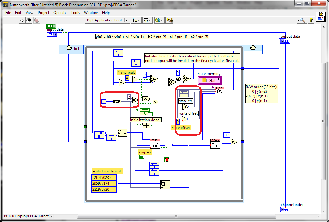
FPGA Butterworth filter - why conversions to decimal fixed?
I was looking through the screw FPGA Butterworth filter Express and stumbled on this code (after conversion the Express VI into a Subvi and then by opening the front panel):
What is happening with the conversion to decimal fixed values that look like they must be integers (in the red boxes)? Why these conversions would be useful?
Here is the micro-optimisations to help the synthesis tools to minimize the number of bits used in these code paths. The iteration Terminal is 32 bits wide and also involves a logic to do in the face of what is happening when the maximum value is reached. We have seen some benefits from the reduction of this path to the minimum width required both that which is written. I think it is probably still the case since the compiler usually does not know how many times a given line will run with a dynamic stop like this condition.
The optimization of the meter width is similar, taking advantage of the fact that we know that we have limited storage space to use circular buffers power-of-2 size. Using the exact number of bits of the address allows us to implement a counter of reversal with no additional logic. otherwise, we would need to check the value, and add a mux (Select) to reset the counter when it reaches the maximum value.
Synthesis tools usually do a good job of optimizing the unused bits, but here are two cases where we can help them by being more explicit about what we really need.
-
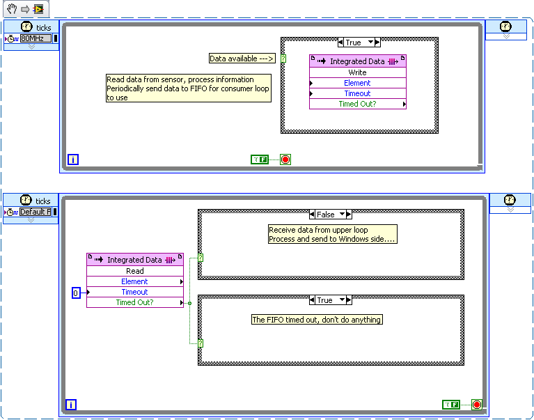
Synchronization between two periods loops FPGA
First of all, I appreciate the forums here and have read a lot of interesting topics. This is the first time I can't solve it with research and I hope for your entry.
Information:
I'm using LabVIEW 2009 f3, PXI-1033 with the PXI-7813R.
Problem:
In my FPGA program, I have two loops, where you need to run as fast as possible (has) and the second just quickly (B). Has turns 20 MHz to 40 MHz and B . These are for the two loops limiting speeds. B cannot run faster and Has should not run more slowly.
Loop has captures the sensory information and integrates data as many loops as indicated by the user. When completed, please send a trigger to B, which calculates the new position information and sends it to the machine. Only at certain times, B must achieve something and said nothing to the rest of the time.I thought of two ways, but doesn't work for me.
(i) with the help of a Boolean trigger. As in a loop, the Boolean value of A can become true and switches to the next loop to false, B is not capture all the triggers and a 50% chance of getting the triggers and isn't perfectly synchronized.
(II) using the occurrences. Sounds very interesting, but these are prohibited between the periods differently loops.
I played with many scenarios, but may not understand proper. Someone at - it suggestions?
This seems to be a fairly simple producer/consumer scenario.
I would like to use a device worn FIFO to transfer data from the loop of producer (top) to the loop of consumer (bottom).
Depending on how often the producer generates data (each cycle or every nth cycle?) the case around the write FIFO structure will allow him to write only when your requirements are met.
The consumer loop reads the FIFO with a timeout of '0 '. When the FIFO is to expire, the consumer runs to the case which does nothing. When the FIFO does not expire, who processes the data and sends it to the side of Windows runs.
In my example, I used 2 structures of cases to illustrate the two different modes. In your code, you must use a single structure of matter.
There is no advantage to set a loop "sleep", even if no data exists on the FPGA. Because you are running in hardware and the non-profit CPU cycles these loops can operate simultaneously at no increase in the latency of a
-
Trigger two FPGA instances at the same time
I have a basic FPGA code that transmits the bits of data on a serial (RS-485) bus, the code is written so that it expects in the first State of a machine to States in a single-cycle timed loop. After a certain trigger, he begins to read a FIFO containing data and sends the data on a line of Tx. It does this until all bits are send and then it goes back to the first State to wait for the next trigger. The relaxation is necessary because windows must fill out first before the FPGA FIFO can start sending.
I need two instances of this code runs, because I have two buses of com (one is redundant). So I use the FPGA code as a Subvi and I wrote a main FPGA vi to call two separate instances of the Subvi in parallel. A regular window vi wrote on the FIFO for bed FIFO for Rx and Tx. No problems so far.
The thing is I start two transmissions in 200nS of each other (Yes, nanoseconds). Windows will write two FIFO in parallel, but the timing is 4uS apart, too long. I tried implementing a Boolean flag in the Subvi FPGA, but windows can not write directly on the control of Subvi. FPGA won't allow (the Write function is grayed out). I tried to use a FIFO for a flag, but the problem is a race condition. One of the instances is first read FIFO and he destroy. The other can't read. I need a common trigger point to be used by the two instances of Subvi.
My final solution was to use a memory in the Subvi FPGA and digital control in the main FPGA vi. Windows write in numerical order, it may because the control is in the main FPGA vi. Inside the main FPGA, I run a timed loop that looks for digital to be zero. If so, it writes the value into the location of the memory used by the Subvi FPGA. After awhile, the principal wrote a zero back to memory to prevent the Subvi is restarted, as well as to write a zero for digital to reset. This repeats, waiting for windows to write in digital again for the next transmission.
I had to do it this way because sometimes I want to pass on the bus, and sometimes just one or the other. Numeric values are used to determine which to pass on. Now, the transmissions are starting to almost exactly at the same time, 1 or 2 nanoseconds apart. But the trigger process seems very silly to me. I was wondering if there is a better solution. I'm pretty new to FPGA.
tbob wrote:
Basically, I did the same thing using FPGA memory. Windows I am writing for a digital control that resides inside the main FPGA vi. In the main FPGA, I write in the memory. Inside the Subvi FPGA, I read the brief and decode the value to use either one or the other or both buses. After fool with it for awhile, because reading Memeory needs to use a shift register (probably because it takes a whole cycle of clock), I had to work. The two bus trigger at the same time. I guess it's not really important if I use a FIFO or if I use the memory. The main problem is that I write Windows at the hand of FPGA, then the hand of FPGA for the Subvi FPGA. Then the time is right for what is the Subvi is.
There are some advantages to the use of two FIFO on your approach. First of all, you don't have the change of register for the memory location. Secondly, we should not worry that VI is responsible for compensation to the memory location, or do, you run the risk that one of your subVIs run twice, or not at all, if the memory is not erased at the right time. Perhaps most important, you'll save yourself space on the FPGA because you will not need arbitration - the additional code that is added when two parts of the FPGA try to access the same resource at the same time. In your case, both instances of the Subvi access the memory block at the same time, so the FPGA compiler adds additional logic to avoid conflict. If only read you the memory block in one place and just write it in one place (reading and writing can be different loops where subVIs) there is no need for arbitration. Using two FIFOs, you can keep independent and avoid the conflict resolution code. See the help for the "arbitration" for more details.
-
Take advantage of the desktop connection using a Wi - Fi connection?
My Mac Mini is connected to my router via a network cable directly by Wi - Fi. I am considering the turn off Wi - Fi because it offers another point of entry for the pirates. If I have understood correctly, Wi - Fi is required to get my location to the map application. Are there other benefits or the inherent risk to it takes precedence over any advantage?
Thank you.
Ethernet is usually faster than wifi.
Yes, wifi is necessary to locate the computer... However, once you have used wifi Mac to remember its location.
As you say, the wifi is a possible door. However, it has more to do with the network rather than individual computers. If you only turn off wifi on Mac and let the wifi on your router that is little or no improvement
-
I have an iMac, but no other Apple product, and given the long list of problems on the pages of the community regarding the update for Sierra, is there an advantage to update me?
You won't see anything, but the problems reported here most of the time. This is a support forum. People without problems, much more numerous than those having problems, but they are not seeking this community to report this fact.
I have updated both my 2014 11 "MBA and my iMac 2011. No real problem. Performance on the iMac has been well below normal after the upgrade, but pretty much a reboot fixed that.
Maybe you are looking for
-
in WRT54GC 5dBi antenna - how to tie
Hi all I recently bought a 5dBi antenna for my WRT54GC router. However, I don't check if the router's original antenna is detachable and unfortunately is not. Does anyone know if there is another way to attach the new antenna or if I'm missing someth
-
Downloaded Samsung PC Share Manager
Manager for my desktop computer (Windows Vista) can share data with my new Samsung 3D TV and 3D Blu - Ray player Sumsung, I am required to download Samsung PC share. However, they say that it is downloadable only for 32-bit machines, while mine is a
-
I can't create new folders in the libraries.
When I click on the button new file that does nothing, does anyone know where I can begin to understand this? No matter if I am in my library of documents or photos, I can't create a new folder for my articles. Thank you!
-
Problem of Smartphones blackBerry 6.0 updated
I just upgraded to 6.0 on 9700 and since I was not able to use the phone. It always freezes on me and wont even work at all with the SIM inserted. Out the sim card and it only that freeze. It responds only to his own will. Tried to re-login to the de
-
On a form, we have a series of fields that contain calculations that the user fills out as they tab through. (works fine) They are mandatory fields.The next section (radio button) asking a simple yes/no question with a conditional under text field. A