Compilation of SCTL loops
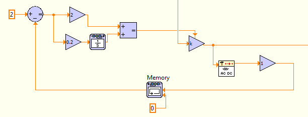
I have a large application FlexRIO FPGA requiring mapping of the various sources of input running at 200 MHz. originally, we had a code that has conducted any mapping entry, but it was the code that had been parallelized manually (which makes quite complex) and had only two possible sources. I had to add a third possible source our code. Thinking that my understanding of loops inside of loops For SCTL was OK, I changed the design of an implementation of loop (attached).
I think I know what a loop size For fixed in a SCTL would be held by the compiler (except all the features not supported as points of coercion or structures) not supported. With the attached design, my compilation is successful. However, when I add this loop to the rest of my code (replace a couple of controls with the registry items), I seem to meet Timing Violations of components non-diagramme. The values of x max being quite high during the compilation fails, I suspect that x is the cause of the failure.
I tried a few different steps to try to get my design compile (including manually try to parallelize the loop For 4 loops, each 8-element arrays of automatic indexing and adding a step in pipeline before the result of the concatenation). Does anyone have any suggestions or advice?
Tags: NI Software
Similar Questions
-
Cannot compile control & Simulation loop
Hi, I am trying to compile a simulation, and the problem is a feedback loop
which is not accepted.
I want to write a program that removes the signal of its DC component and controls the amplitude of the remaining AC signal
Thanks to a feedbackloop. The PI-regulator controls the gain of an amplifier.
Hello laskar01,
Instead of the feedback, use VI memory node. Your problem should be solved.
-
An associative array, how the records using the loop counter?
In the associative array, how the records using the loop counter? for example
declare
    type population is table of number index by varchar2(64);
    city_population population;
begin
    city_population('Samillve') := 200;
    city_population('Lindenhurst') := 300;

    for i in 1 .. city_population.count
    loop
        dbms_output.put_line(city_population(i)); -- compiler error
    end loop;
end;
/
That would look like
SQL> ed
Wrote file afiedt.buf

  1  declare
  2      type population is table of number index by varchar2(64);
  3      city_population population;
  4      l_index varchar2(64);
  5  begin
  6      city_population('Samillve') := 200;
  7      city_population('Lindenhurst') := 300;
  8      l_index := city_population.first;
  9      while( l_index IS NOT NULL )
 10      loop
 11          dbms_output.put_line(city_population(l_index ));
 12          l_index := city_population.next(l_index);
 13      end loop;
 14* end;
SQL> /
300
200

PL/SQL procedure successfully completed.
Justin
-
I try to use NI 9870 with a loop timed in FPGA programming. I have the output defined in the FPGA program and the host program that I'm reading the given recived. However, my host is a loop timed with 3ms loop timer. I read recently that NI 9870 can't Timed single Cycle (SCTLs) loop in the FPGA. Is this true? is there a way to get around this?
Kamal
A SCTL on fpga requires the code to run in a single cycle, so at 40 Mhz, it comes to 25nS. not a lot of modules support this mainly due to transfer of data to the module. Your 8970 can easily stand 3mS loop rates, simply use a while loop and loop timer. what I don't understand is that say you that the host has a timed loop 3ms. How do you transfer data to the FPGA? I suggest maybe a DMA, then the FPGA knows nothing of the synchronization, it sends data just when she has something in the dma (-1 timeout on FPGA dma read, no timer necessary loop) on the 9870 think time-out settings in the properties of the module, and use a node to call to check the errors CAN without these the node of your writing could easily hang indefinitely if there are errors on the CAN bus. In the Finder of the example, there is a good example of sending data by querying the controls FPGA which is also a good method.
I hope this helps.
Michael.
-
Cannot use Select inside the loop For inside the SCTL (FPGA) - Bug? An alternative?
When I put a Select statement inside a loop in a loop of Timed Cycle in LabVIEW FPGA, I get the following error when I try to compile:
"An internal software error occurred. Please contact National Instruments technical support on ni.com/support with the following information:
Error-61003 occurred at
Possible reasons:
LabVIEW FPGA: you cannot include this function in a loop For when the loop is within a single cycle timed loop. »
I didn't know that whatever it is documented that says that this is not allowed; is this a bug or am I missing some documents?
The code that causes this error looks like this, inside a SCTL (ignore Boolean wire wandering behind the loop for)
I came up with the code below instead, which compiles into one Cycle timed loop, but it is a bit ugly. Does anyone have a better suggestion?
This issue is currently followed under the CAR # 592391. Please keep an eye on our patches and new versions as usual!
-
FPGA timing when compiling PID loop error
Hello.
I'm using Labview 2011 card FPGA PCI-7833R.
My problem is that whenever I try to integrate FPGA designed screws in my code, I get an error of timing. See the photos displayed below.
In this case, I have an express VI PID which I use in a used while loop (not even timed!) in my FPGA code, but when compiling, I get an error saying that the possible maximum clock frequency is the 43 MHz.
I have a lot of loops, a few running at 80 MHz. Is there a way to slow down a specific while loop, so that it runs at 40 MHz and not 80 MHz, as others? The compiler does not seem to meet the simple addition of a timer loop...
Thank you
Orel.
PS the same thing happens when I try to add a lowpass filter VI of the FPGA code.
Is it possible that you set the level above 80 Mhz clock? This is what it looks like to me. In Explorer, right click on the FPGA target, select Properties, then go to the category "first level clock.
-
The condition of the Terminal loop in a wiring SCTL
Hi all.
I'm relatively new to LabVIEW, and I have a little doubt with a Terminal loop condition which I think is pretty basic. When using a while loop, the VI breaks if there is no condition connected to the Terminal, even if it is a constant t. The same is also pretty explicitly mentioned hereand I think that makes perfect sense.
Now, I am interested in some code LabVIEW FPGA on a forum post that I was living to understand better SCTLs (only the attached photo is NOT my own code, credits to Mahesh0459), and the conditional terminal in the SCTLs does not seem to be wired. When I watched the video that introduced this concept, loop a while turns out be replaced directly with a SCTL, whereupon the F constant (since the while loop) is automatically connected to the Terminal.
So, my question is this: is it a good idea to leave the condition of the Terminal loop unwired in an FPGA VI? If so, what is the reason? Alternatively, is this SCTLs-specific behavior? If so, again, what is the reason?
Thank you!
Only in FPGA is fine. The reason being that it is assumed the loop will only run for always in the material. No no not the loop control registers some doors.
-
How to calculate the execution time of a SCTL in FPGA VI?
Hello
Can someone guide me that how to calculate the execution time of a SCTL for an iteration in the FPGA VI?
Thank you and best regards,
Rashid
Hello r,.
A SCTL will always run in a beat the clock it has been linked to. So, if you use a 40 MHz clock, this loop will run in 25 ns. If the code cannot complete in that, or if it requires two graduations of the watch to do the calculation, your code does not compile, then you have the guarantee that this will always be how long it takes this piece of code to run.
-
LabVIEW FPGA: Problem compiling look-up Table
Current versions of software:
LabVIEW 2014 SP1
LabVIEW FPGA 2014
Xilinx Vivado
I'm having a huge problem in trying to compile my LabVIEW FPGA code.
Some recall of the code:
It's all in a SCTL.
I am streaming in a FIFO DMA and comparing it with the values previously stored in the shift registers (which are initialized to 0 at the start of the loop) in the SCTL.
The results of the comparison are then piled into a U16 and loaded into a lookup table (I use the LUT - 1 d), and I'm so help this LUT to decide what value will be charged to travel to record for the next iteration of the loop, which, in any case, would be either the current values of the flow, or the post previous registry value.
(It's a triage loop)
I am able to run very well in simulation mode code, but when I try to compile, I get this error:
"The selected object has a built-in shift register that makes the output on a particular loop iteration correspond to the entries in the previous iteration."
Connect the outputs of the object directly to a minimum number of nodes of Feedback or uninitialized shift registers. You cannot connect the outputs to another object.
See using LabVIEW for more information on the objects with registers embedded offset. »
Someone at - it ideas why this happens, and what might be the possible solutions?
I'm tempted to break it down into separate loops, but I prefer not to because it is now a loop (and working in my simulation).
I found my problem.
Any time that a LUT is in a chain shift register, it cannot:
1. be part of a string of shift register that has a variable initialized
2. follow-up to no decisive structure, like a box structure.
I just moved the position of LUT and it works.
-
Violation of timing when adding code blocks parallel to each other in a FPGA SCTL
Hey guys!
I have a problem with my code inside a SCTL of running on an FPGA VI and hoped someone could help me.
I work with a 120 MS/s ADC and write the data to the FPGA block of memory in a 120 MHz SCTL. Since the data has to be 'mixed' there is also a code to get the correct address (by first example data at address 0, second to address 20, 40 and so on until 2000, then I start with 1, 21...).
I have a second block of code that later, when writing is completed, reads in the block of memory to perform some calculations (a linear slope of the signal interpolation)
The two parties are implemented using pipelining (I say this because I think it would be the first response of the community), while if I compile only one, everyone needs about 7 to 8 ns to run, which means that they meet the requirements to run in my 120 MHz SCTL (8.33 ns).
But when two blocks of code are in the same field of clock (whether in ore SCTL in two SCTLs using the same clock) from the FPGA VI I get a timing violation, saying that the code in the SCTL needs 17 ns (logical and delay routing) to run. It is not also show me the critcal way, just the SCTL. Because the code runs at the same time, I don't see why the delay of logic should increase (to 12 ns). The only way 2 code blocks communicate with each other are the memory of block and some shift registers so the path of Combinatorics is not increased.
I already checked whether the SubVIs (I use one per block of code to avoid the lack of clarity, but they are different) are the problem. If the code in the SubVIs implemented directly in the FPGA hand VI it does not change the delay of logic.
50% of the registers and the lut FPGA are used, the DSP48s of 5% and 50% of RAM block, so I don't think that the problem is something like the compiler finds not enough free slices to create fast paths.
The main problem is not that the delay of routing increases, but the delay of logic.
Does anyone have an idea what could cause this huge increase by delay time?
I use labview 2011 and 12.4 Xilinx.
Try not to put memory read the node within a box structure. Instead, you can always read from a fixed address, say 0, when the data are not all ready. Reading a memory will not damage your data contrary to push from a FIFO. If your memory by reading the node is inside a case structure, there will be a mux when data is passed outside this business structure, which will increase the delay of logic.
In addition, I also recommend that you do not use the loop of the index 'i', if you are running at high clock frequency. This counter is seen to be 32-bit, and you probably don't have a memory that deeply. LV FPGA is to have logic check inside the read node memory address range, so width incorrect address can still be important. You can implement instead of your counter code which the width of the tip is appropriate.
-
Using the C-series SCTL DIO module with slower than the top level [FPGA] clock
Hey all,.
I'm running online research on a problem that I have a lot of success.
I have a chassis with integrated FPGA, top-level 9030 clock 40 MHz. I have a NOR-9401 DIO C Series module plugged and the value that will be managed by the FPGA target. I need to count some linear encoders to exactly 10 MHz, no more, no less. They are periods and gives a result of such kind that if I oversample or underestimate, I get garbage.
If I create a SCTL and assign a source of synchronization derived from 10 MHz, I get an error code generation who:
"Node read e/s for DIO3 FPGA is used in a clock domain that it does not support. Areas of clock supported include: the clock of higher and clocks that have a rate that is a multiple of 40 MHz, for example 40 MHz, 80 MHz, 120 MHz and so on. »
I tried several ways to work around this problem; First I tried just using a while loop with a loop set to 4 is ticking timer, but it then takes 9 clock cycles to perform the count for a reason any (although this code may compile in the SCTL without any problem). I then tried to use the SCTL with a constant of 'true' AS a hack for a 'timed sequence' framework-related, and that certainly has not worked.
Are there any strategies or techniques, or settings somewhere to work around this limitation on the AID I need to taste exactly 10 MHz? I'd like to do this quickly in the software and get this rolling as soon as POSSIBLE.
An image of the relevant section of the code is attached, I'm happy to provide you more things on request.
Thank you very much!
Maia Bageant
Thanks for the reply! The problem ended up being a hardware problem based on how coders were connected. Now that I've fixed it, they're perfectly happy are oversampled.
I guess my question is always legitimate to other applications, but not necessary for encoders a.
-
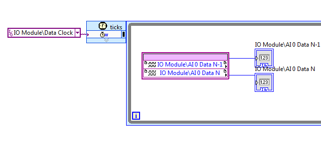
Module e/s NI 5761 clock compiled 0 to 100 MHz in single/multiple Sample CLIP examples of projects
Hello
I was trying to wrap my head around the CLIP sample NI 5761 Multi (v4.1.0) because the CLIP provides 250 PSM data, but the IO module requires a clock of 200 MHz. I think, ' NOR should handle the conversion of the clock, fine, but I hope that the diagram is running at 125 MHz... otherwise I'm really confused "so I look at configuring the clock Module e/s in
0 \examples\FlexRIO\IO Modules\NI 5761\NI Getting Started\NI 5761 5761 - to Started.lvproj and to my surprise, it is compiled for 100 MHz. I checked the target 7965 in NI 5761 single sample CLIP\NI 5761 - unique CLIP.lvproj and IO Module clock 0 sample was compiled for 100 MHz there as well.
I do not understand the difference between the flow of data and the selection of clock 200 MHz IO module, and it would be nice to understand it, but not necessary. Also, I don't understand the difference between data rate and the configuration of the Module e/s 0 clock that drives the SCTL that contains the node IO. I understand that to move forward.
Thanks for any help,
Steve K
The CLK200 in the selections of the clock is used to excite the parts of the fixed logic that are internal to the CLIP. Some CLIPs FlexRIO may only require a CLK40, this one requires a CLK40 and fixed a CLK200 to properly perform its logic. Thus, it seems that everything is ok in regards to that.
Unfortunately, the example incorrectly uses IOModClock0. The SCTL AI IO node resides in should use a resource of the clock that says "Data Clock. We've updated the examples in more recent versions of the pilot, but you seem to be using a version of the driver where a CLIP that uses the clock of data is the latest available for the 5761 CLIP, but the example has not yet been udpated to use.
-
How to reduce the length of loop of HP
Hello
I'm running a model with a rate of 5 kHz in a quad core 2 to 2.6 GHz computer.
If I put in "parallel" run mode model County is growing rapidly but the model rate keeps at 5 kHz.
Changing the mode of execution of "Low latency" model remains at 0, rate model County goes to 2.5 kHz and increases the number of HP.
The total allocation of processor of each carrot never passes over 58% in "Low latency" but reached 98% in "parallel".
I tried several combinations of basic allowances (auto / manual) for loops and model, but the main factor is always to run mode.
I have observed that, when you use a low latency, the length of loop of HP reached 218000 ns which explains why the model rate drops.
Is there another setting I can use to leave the system without cost overruns?
See you soon,.
Claudio H.
Hello
I managed to include optimization during code generation options.
In the Simulation > Configuration settings > RealTime workshop > NI Configuration > compiler optimizations, I put "To promote a quick code" and got:
-size of the dll from 452 kb to 404 KB
-Model occupation CPU loop from 98% to 82%
-7% to 23% control loop
-Data loop ranging from 8% to 49%
-Account template more fast to very slow.
It seems that now the model works more time and loop control and loop data have more work.
We will work in the model to make it easier we can.
See you soon.
-
Compilation failed due to an error of Xilinx.
I've recently updated since LV2014 until 2015, and an FPGA VI who previously compiled successfully is no longer made. My goal is a 7951R and I use a module e/s of 6584. A few minutes in the compilation process, I get the below error. I found the White Book of OR describing this problem for 2010 and provide a patch, but this solution has failed for me. Curiously, I can succeed in the compilation of FPGAS screws very simple, but not more complex that were previously viable.
LabVIEW FPGA: Compilation failed due to an error of Xilinx.
Details:
ERROR: HDLCompiler:432 - "C:\NIFPGA\jobs\ODf62Gx_H0cwa34\NiFpgaAG_0000023b_ForLoop.vhd" line 55: Formalhas no real or default value.
INFO: HDLCompiler:1408 - "C:\NIFPGA\jobs\ODf62Gx_H0cwa34\arrayLpIndx_593.vhd", line 22. array_in is declared here
ERROR: HDLCompiler:854 - "C:\NIFPGA\jobs\ODf62Gx_H0cwa34\NiFpgaAG_0000023b_ForLoop.vhd", line 24:Unit ignored due to previous errors.
File VHDL C:\NIFPGA\jobs\ODf62Gx_H0cwa34\NiFpgaAG_0000023b_ForLoop.vhd ignored errors
-->Total memory use is 239156 kilobytes
Number of errors: 2 (filtered 0)
Number of warnings: 11 (filtered 0)
Number of news: 0 (0 filtered)"Synthesize - XST" process failed
Compile time
---------------------------
Introduction date: 04/12/2015-16:36
Date recovered results: 04/12/2015-16:38
Waiting time in the queue: 00:09
Compilation of time: 01:44
-Generate a Xilinx IP: 00:00
-Estimate of the resources - PlanAhead: 00:33
-Summarize - XST: 00:56Okay, that was weird.
I discovered there was a small change between revisions. I had wrong initalized a table by exchanging the entries, so that the size of the array is 0 instead of n. normally, this should be taken at the beginning of the compilation, but this table null was used to initialize a shift register in a while loop and the exit from the while loop enters a loop, where my FIFOs operate. While the loop/shift register seems to be the essential element to the compilation of progress as he did and present it as a mistake of Xilinx. If you delete the while loop then the error is detected quickly and correctly identified.
-
FPGA IO node and loop Question of Timing
I'm having a lot of trouble to compile a very simple FPGA VI for a system for the acquisition of data on my cRIO (9075, using a single module 9205 cRIO, labview 2012 dev suite, xlinx13).
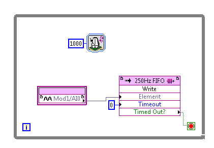
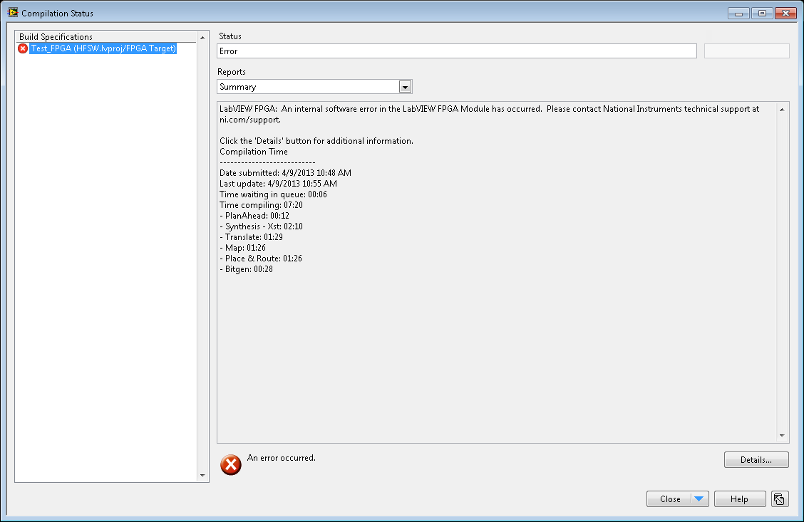
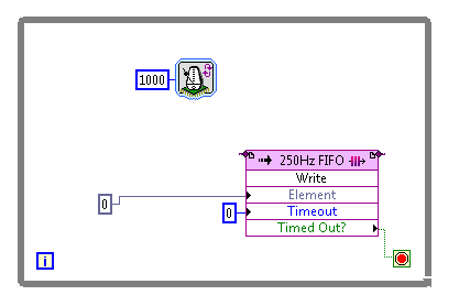
At the end of compilation, the error occurs if and only if I use a block of i/o node FPGA. This picture shows my very simple VI which fails to a compilation:
When I compile, I get this error at the end:
And here are the details of the error:
It is also interesting to note that the 'Timing' summary says I need a clock of 80 MHz, when the on-board clock of 40 MHz.
For comparison, when I remove the FPGA of e/s node and replace it with a constant, the compilation succeeds:
The need of a clock of 80 MHz disappears also, according to the report of timing.
Is this a problem with how loops work in FPGA? I've been reading about "single-cycle timed loops" that guarantee a performance per clock cycle. I don't have that kind of acquisition rate, and I guess the structure of loop, I created is not related to a single cycle because of the block of metronome, that I inserted. I guess correctly? Are there structures of loop for FPGA which is not related to a single clock cycle?
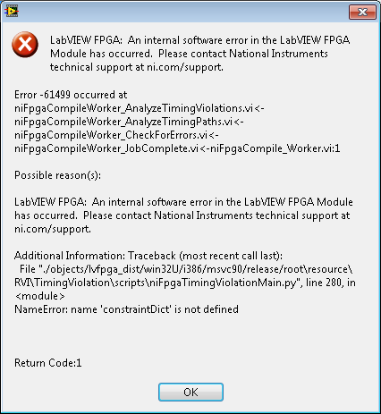
I also wonder if this error is not to do with my code, but is rather an internal error of the software compilation NOR, in particular the 'niFpgaTimingViolation.py' script mentioned in the summary of the detailed errors. I got labview 2011 and xlinx 12 installed on this computer before, but they uninstalled before the upgrade. This is my first project in 2012.
I appreciate the comments of the community NOR. Let me know if my question needs further clarification.
-Andrew
I solved the problem.
In case that someone looking for it later (error 61499 niFpgaTimingViolationMain.py that constraintdict is not defined).
I did a complete uninstall and reinstall my entire LV 2012 dev suite. Then the same VI used to compile failure began to pass compilation. Apparently, I had a corrupt file somewhere.
Maybe you are looking for
-
Satellite Pro L100 CPU upgrade
Hello The hope for some advice. I recently bought a Satellite Pro L100 of second hand, came up with the following configuration. Celeron M 370, 256 MB Ram, 40 GB drive HARD, Win XP As the laptop is out of warranty, I disassembled the laptop and upgra
-
Solid black line on the screen of the HP Tablet
I just got this HP 7 5709 flow. So far so good except there is a horizontal black line across the screen. I first thought, this is the screen protector, but now I'm starting to think that it is in the screen itself. Is - is this known? Attached to th
-
Replication over 1 GB for remote data center links
I Compellent LUN in a city and you want to replicate to a Compellent storage array in another city. We only link to 1 GB and 500 GB of data to be replicated. I guess an asynchronous replication would be necessary, but you should know how it will affe
-
HOW can I get the code for CORRECTION of ERROR 39?
IM really hoping that someone out there in PC-land can help! I have a problem with my CD/dvd-rom drive. the D of DVD LITE-ON LH-16D1P ATA device' installed when I bought my PC has the yellow triangle on him when I access my device manager. the driver
-
Impossible to get the specific features of cisco in LMS syslogs
Hello It's about a problem that we face with our LMS 3.2.1. We cannot get specific cisco devices syslogs, while we are able to get the rest devices syslogs. one you suggest what would be the exact reason for this and the troubleshooting steps. Thanks