Exhibitor block signal - Xilinx FFT v7.1 - FlexRIO - FPGA
I use Xilinx FFT v7.1 IP (FPGA - OR 7965R, LabVIEW 2012). I am computing the FFT of real integer 16 bit signed.
Bit 5 signal exposing block block floating point FFT in module v7.1 Xilinx FFT signed or unsigned? Pdf document talks shift to the right of the data output to use the dynamic range, mentions not moving to the left, neither gives sufficient detail on this subject.
Is there a base value as format IEEE floating point should I use to find the correct output value?
I guess that it is unsigned unless you have comments to the contrary. The basic behavior is to keep bits on the left in order to prevent any overflow, so the scale always implies move on to when you think that some of the more significant bits are unused. They provide an example of b00101 = 5, so that indicates there is no bias to apply.
Tags: NI Hardware
Similar Questions
-
Xilinx FFT IP 7.1 (equivalent of 4-wire Handshaking)
Hi all
I'm trying to figure out how to get the IP of 7.1 Xilinx FFT to handshake properly as the 4-wire LabVIEW FPGA FFT Express VI. I need the use of Xilinx FFT because of the constraint of maximum length 8192 on vi express.
The common 4-wire for the handshake are:
ENTRY: entry valid
ENTRY: ready for the output
EXIT: exit valid
RELEASED: ready for the entrance
The Xilinx includes a few pins that are similar such as
OUTPUT: valid data
RELEASED: ready for data
OUTPUT: fact/edoné
ENTRY: Activate the clock?
Any ideas on the pins, I can use as INPUTS: input valid and ready for printing?
Thanks a bunch
Hi Jeffrey,.
I have attached an image I hope you find it useful.
Valid entry will match the activation (EC) clock pin
Output valid with valid data (dv) and
ready for the entrance with ready for data (rfd)
Let us know if you have any other questions.
Thank you
-
Programming a module FlexRIO FPGA to computer?
Hello
I'm new to National Instruments LabVIEW equipment. I have a FPGA FlexRIO SMU-7965R module and a RF Transceiver 5791.
To use this equipment, do I have to have a chassis (to put my FPGA), or can I simply program the FPGA on my computer (using a cable)?
João
Hi João,.
You should always at least a SMU chassis with a controller. The SMU-7965R Board is like a PCIe card only a different form factor. You must put it in a slot SMU as you need to put a PCIe card in a PCIe location.
I suggest trying the PXI Advisor to see what type of systems, you can use. PXI Advisor
Choose your Board under Modules, then only supported chassis and controllers will be available.
When you choose to create a LabVIEW project with the jury FlexRIO (FPGA target) in my computer, you specify that you will use the FPGA target with a Windows host.
Here's an introduction to LabVIEW FPGA Webcast:
http://www.NI.com/Webcast/240/en/
Best regards
Klas Andersson
National Instruments
Support
-
Extrapolation of signal with FFT
Hello
I want to extrapolate (generate some outter points a signal given).
My approach is to use a FFT to acquire the signal spectrum,
and, to go back to the time domain of the iFFT to generate the new signal.
But there is no option (iFFT) to specify the size of the generated signal.
For example, if I have a signal of 1 Hz with Fourier, I must be able to generate a signal with an arbitrary length.
Is there a function in LV that generate a signal of varying size for each of Fourier Coef gived in entrance (by the FFT)?
Best regards
Nicolas
-
Automatic Orientation of blocking signal
Hello!
I've developed an application, that is opposable by other applications. At the call of my application, it is launched in a map (at least I guess). Is it possible to block the signal of automatic orientation or lock the screen in portrait mode?
This is what I tried in QML, and which does not:
onCreationCompleted: {
      OrientationSupport.supportedDisplayOrientation =
      SupportedDisplayOrientation.DisplayPortrait;
}
Any help is appreciated!
Thanks in advance :-)
in the cards, you have to manage the change of orientation.
-
Violation of timing when adding code blocks parallel to each other in a FPGA SCTL
Hey guys!
I have a problem with my code inside a SCTL of running on an FPGA VI and hoped someone could help me.
I work with a 120 MS/s ADC and write the data to the FPGA block of memory in a 120 MHz SCTL. Since the data has to be 'mixed' there is also a code to get the correct address (by first example data at address 0, second to address 20, 40 and so on until 2000, then I start with 1, 21...).
I have a second block of code that later, when writing is completed, reads in the block of memory to perform some calculations (a linear slope of the signal interpolation)
The two parties are implemented using pipelining (I say this because I think it would be the first response of the community), while if I compile only one, everyone needs about 7 to 8 ns to run, which means that they meet the requirements to run in my 120 MHz SCTL (8.33 ns).
But when two blocks of code are in the same field of clock (whether in ore SCTL in two SCTLs using the same clock) from the FPGA VI I get a timing violation, saying that the code in the SCTL needs 17 ns (logical and delay routing) to run. It is not also show me the critcal way, just the SCTL. Because the code runs at the same time, I don't see why the delay of logic should increase (to 12 ns). The only way 2 code blocks communicate with each other are the memory of block and some shift registers so the path of Combinatorics is not increased.
I already checked whether the SubVIs (I use one per block of code to avoid the lack of clarity, but they are different) are the problem. If the code in the SubVIs implemented directly in the FPGA hand VI it does not change the delay of logic.
50% of the registers and the lut FPGA are used, the DSP48s of 5% and 50% of RAM block, so I don't think that the problem is something like the compiler finds not enough free slices to create fast paths.
The main problem is not that the delay of routing increases, but the delay of logic.
Does anyone have an idea what could cause this huge increase by delay time?
I use labview 2011 and 12.4 Xilinx.
Try not to put memory read the node within a box structure. Instead, you can always read from a fixed address, say 0, when the data are not all ready. Reading a memory will not damage your data contrary to push from a FIFO. If your memory by reading the node is inside a case structure, there will be a mux when data is passed outside this business structure, which will increase the delay of logic.
In addition, I also recommend that you do not use the loop of the index 'i', if you are running at high clock frequency. This counter is seen to be 32-bit, and you probably don't have a memory that deeply. LV FPGA is to have logic check inside the read node memory address range, so width incorrect address can still be important. You can implement instead of your counter code which the width of the tip is appropriate.
-
Model a block synchronous dual-port RAM with LabVIEW FPGA
This question caught my attention recently.
I am trying to model a particular design element called "RAMB4_S8_S8" with the LabVIEW FPGA module. This element is a block synchronous dual-port RAM allowing simultaneous access to two ports independently from each other. That being said, a port can perform read/write operation to this RAM while at the same time, the other port might be able to do the same thing. There are two opportunities of possible port conflict, however. The first is when both ports are trying to write to the same memory cell. The other scenario is when a port writes in a cell memory while at the same time the other port reads from it. Other than that, everything should be a legitimate operation.
In order to reproduce this I select memory block that is integrated into my FPGA target. An interface is configured to be the playback mode, and the other is set to write fashion. For the option of arbitration, I let the two interfaces to be "arbitrate if several applicants only. Then I got a compiler error when I tried to run my FPGA code for this model in a SCTL. The error message is something like "several objects to request access to a resource through a resource configured with option interface" arbitrate if several applicants only ", which is supported only in the single-cycle Timed loop if there is only a single applicant by interface.
This error goes away if I replace the SCTL with a simple while loop, but not what I would like to implement. So I wonder if there is a better solution to this problem, or is it just the limitation of the LabVIEW FPGA module.
Thank you.
Yes, you can use a form of conduct to perform the operations you want in the generations clock cycles, but all the code is inside a single SCTL. Basically, read the first address and storing in a register in a single cycle and then read the second address in the second clock cycle. This would allow you to two readings of valid memory every clock cycle 2. I have included a crude extract to illustrate the concept. The case selectors are identical with address A being connected to the memory in the true case, B in the case of fake address. Your biggest model memory dual port will be intact, but it will operate at 1/2 rate.
Take a look at the white paper that provides more details on the construction of memory:
Data on a target FPGAS (FPGA Module)
The ball on the memory block indicates that memory block double port cannot be applied in a configuration of reading, which is a double ROM. access read/write port must be imitated with custom code.
-
Compilation of Xilinx not installed labview 2015 FPGA tools
Hello
I just installed Labview 2015 + FPGA Module on my computer with an older version of Labview 8.6.
When I compile a labview FPGA project 2015 I got this error message "year error occurred while communicating with the server compilation" and warning "tools of Compilation of Xilinx not installed."
I can assure you that my server of 2015 lunch perfectly and I installed everything correctly. I assure that it is a conflict between labview 8.6 and 2015 therefore uninstalled the older one.
The problem is my build configuration is set to Xilinx 10.1 (which should be 14.7) and there is no way to change this.
After looking around I found that Labview looking for best compilation tools then maybe this is not the problem
Is there something I missed?
Kind regards
Hello
I found the source of the problem. The FPGA, I used was based on a FPGA Virtex II matrix that is not compatible with this version of the build tools.
Thanks for helping me!
-
Should I reset the FPGA FFT when changing the input signal?
Hello
I have an application based FlexRIO where I do FFT on several incoming signals. The signals will be ranked so that I get first for example 4096 samples of Ch1 and Ch2 4096 samples, etc. This means that I don't have to do it in parallel of the FFT and I would like to reuse the implementation of FFT and windowing to reduce the use of resources.
I intend using the VI Express followed by the Express VI of FFT window scaling
http://zone.NI.com/reference/en-XX/help/371599J-01/lvfpga/fpga_scaled_window/
http://zone.NI.com/reference/en-XX/help/371599J-01/lvfpga/fpga_fft/
and I'll use them inside a SCTL.
This figure comes from the section using the FFT and help illustrate the issue:
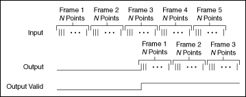
There is a discount to zero terminal for the fenestration and the FFT VI.
Are there internal registers in the windowing and FFT which force the image 1, image 2,... from the same signal or is it possible for the first entry in a framework of Ch1, the next frame belonging to Ch2, Ch3 gaze and so on and always get reliable results?
Another way to ask the same question: if I have to reset the window and FFT when changing the input signal?
Thank you
Anders
Hi Cyphish,
When using the FFT of the LabVIEW FPGA vi express and windows nationwide express vi calculations are make it point by point so there will be no problem when going through different types of measures. Therefore, you should have no problem with your application.
Best regards
Menelaos.K
-
Get the minimum frequency of three signals FFT
Hello
I put in work of a closed online using LABVIEW loop controller. There are three entrances of signal, the FFT of each signal must be calculated online and frequency spectra is the lowest to be detected.
The plot of the Spectra is attached...
Please advice on how to achieve...
Thank you
ruser.
-
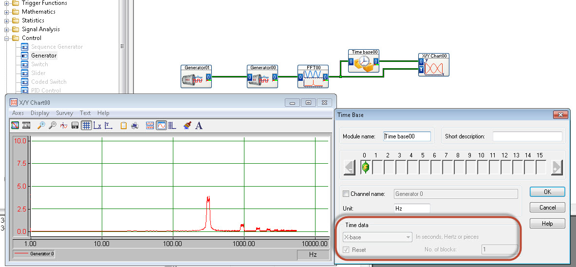
FFT to display with newspaper frequency axis
Hello
I'm trying to get my fft to display frequency (x axis) with a logarithmic scale.
There is no option for this in the table y/t
The xy graph has possibility of HRT, but I cannot "demux" the fft output signal successfully.
I use DasyLab 12.
Someone at - it ideas?
Thank you
Matt
Use the time Base module (special offer) to extract the x axis out of the block of the FFT.
-
Move from LabVIEW FPGA block of ram address to node CLIP?
Hello
I need to pass an index memory RAM of LabVIEW FPGA block to a CLIP node to the node CLIP to have access to the data in the BRAM. The node of the ELEMENT contains an IP address that we developed and the IP address is the use of Xilinx BRAM driver to access data. I guess that we need to move the physical address of the BRAM to the ELEMENT node.
Is this possible? If so, how? If this is not the case, what would be an alternative?
Thank you
Michel
If I understand you correctly, Yes, you should be able to use the memory block of the Xilinx pallet Builder in LabVIEW FPGA and in the loop of the single Cycle, connect the ports of this block signals CLIP exposed by the IP of your colleague. You may need to tweak/adapt some of the signals slightly to the LabVIEW data flow.
-
Multichannel data acquisition and 2D signals
Hello
[Use of labview 2011 license academic with NI9234 and cDAQ-9178].
I'm trying to read, display and record the signals from two isotronic accelerometers and a microphone at the same time for future signal analysis (FFT, etc.). I wish to display data of vibration and noise signals in real-time at 44100 Hz sampling frequency and display a waveform of final sampling, which takes about 40 years. I would like to then write the data to a file.
The associated block diagram, attached vi. I could view real-time each accelerometer and sound using iterations of the loop and split the signal. Unfortunately I record three channels of data in a table unique 1 d-wave form. It seems that the data is saved as iteration1 (ch0) .iteration1 (ch1) .iteration1 (ch2) .iteration2 (ch0) .iteration2 (ch1)... and so on.
Although I could show all three signals separately in the waveform graph, but I prefer these data to save as table 2D-waveform (each channel in a separate column).
I believe that this issue has been raised here (http://ni.lithium.com/t5/LabVIEW/Concatenate-2D-data/td-p/873409) unfortunately no solution has been proposed. How can I record the signals of data acquisition in 2D waveform?
Thank you.
I think to represent vi attached a solution architecture producer consumer for the problem mentioned above. Just thought I'd share to those who can live a similar situation that I had been faced.
-
low Harmonic frequencies in the signal strength
Hi all
I try to know what are the causes of noise in my signal, whether it's a faulty hardware or my lack of knowledge.
The system that I'm actually consist of two engines not to not (parker HV232) that provide the uprising due to frost harmonic + pitch motion with phase shift of 90 degrees (a kind of movement of fish tail beat). I have a load cell 3 - axes attached to the shaft of the motor, pitch, and it measures up, drag and torque on a plateau which oscillates in the tunnel water (oscillation is provided by these two Steps). Tunnel to provide the incoming stream.
Signals of strength are captured through SG-23 + PXI-6221 daq card, I put the gain on the last of them to +/-200 mV for better resolution.
When the engines are turned off, the noise level on the static signal is the threshold of resolution, and nothing strange is not shown in the signal, and its ghosts.
The problems begin when I initialize the motion on the steppers, FFT of the watch signal of the low frequency spikes that are exact multiplies the frequency of oscillation, I have attached a PDF for example.
Disengage amplifier/filter which was suggested by manufacturing, and suspect I have observed could be due to this I'm not sure at 100%. The VI I use filter band-pass data in the 0.2 to 6 Hz, but somehow I can still see noise beyond 6 Hz.
I was wandering perhaps someone has experience with similar issues and can suggest a solution on how to get rid of these harmonics.
Thanks in advance
I'm not an expert in the dynamics of the tunnel, but from what you say, it looks like they can't be noise but components generated due to the rotation of a mechanical Assembly. Normally people refer to these harmonics in the form of 'order', which means that they are a multiple of the frequency of rotation.
So maybe it's the attacker
1. check by an expert (the one that includes the mechanical system that you are using) that to the point where you measure the force will not get the components of the order.
2. understand what exactly is the measurand. What exactly do you want to do with the measured signal (RMS, FFT etc..) Then you will be able to figureout if components of the order may affect your measurement.
Oleks wrote:
Disengage amplifier/filter which was suggested by manufacturing, and suspect I have observed could be due to this I'm not sure at 100%. The VI I use filter band-pass data in the 0.2 to 6 Hz, but somehow I can still see noise beyond 6 Hz.
During filtration, the attenuation in the band determines how fast the signals will be thinning of the hard shoulder.
-
FPGA block memory and Timing FIFO
Hello
I am trying to access the data of the memory block and a FIFO, both having an equal number of elements.
I'm trying to access the data must be coordinated with the waveform of a block of Xilinx, I use to deal with the elements of the FIFO and the memory block.
My block of Xilinx has a 3 clock offset cycle and one without a clock cycle lag, which can lead to my use of knots of late.
My question is, the output of an element of a FIFO occur in a clock or a clock set cycle? Also, I am aware that there is a delay of the output clock cycle
block of memory to hold data into account initial reading, which will lead to my choice of offset of 3 clock cycle. Just a handful to decide how much to delay the nodes to use.See you soon
Hi RichieA
If the function or if it is a FIFO, or a memory block is inside the recycled then timed loop function and of all that is on the inside must be executed in a heartbeat. Don't forget that when you compile you are actually programming and connect a gate array so when the compiler is running, it will try to create the FIFO or memory to be executed on a tick. If this is not possible, you should get an error in NI LabVIEW or in the compilation process. Here is a link with more information.
Single-Cycle timed loop FAQ for the LabVIEW FPGA Module
Concerning
R. Esteban
Maybe you are looking for
-
The "secure" (lock) icon no longer appears on the status bar (or anywhere else I can find) when you go to a secure web page. How can I get the 'secure site' (padlock) icon to display when you access a web page secured with Firefox 4?
-
Equium L20-198 loses time - about 7 minutes each day
My L20-198 system tray clock loses about 7 minutes each day.I can update manually via the "set Date/time" function right click but must remember to do whenever I start and, as often, I forget quickly become desynchronized of 20-30 minutes. Any ideas
-
Driver for Dell 3100cn el capitan
Hello I guess I can use PostScript for IP base for my Dell 3100cn color laser printer network on my new macbook pro El Capitan 10.11.2 but is there a more specific? I use the installer of MFP color Dell 1355 by the suggestion of someone. BTW, how to
-
Photosmart 5510 - wifi ok but not ok ePrint
Hello I got a new 5510 e - all - in - one It is connected to my modem wifi and my 2 laptops are connected too. I can print from my two laptops to the printer, scan is working, etc.. However, I can't implement the ePrint. When I thouch the screen of t
-
OEM product key is invalid for activation.
My Dell Inspiron 1545 is dead. I installed the original ultimate OEM vista on a HP desktop pc. During activation. Now key OEM product not invalid for activation. The original OEM product key is on a single computer only. What I would do.