In the target FPGA read/write control function?
Hi people,
I learn a lot from the sample project FPGA, including how you can easily retrieve and set controls and indicators in an FPGA using the read/write control function running in an RT target.
However, I can't find a way to do something similar in a FPGA target. I've been down this road before - that is, trying to move the data in/out a looping VI FPGA (void) to a (parent) FPGA VI - where my memory points to reach what I needed use.
So I was happy to see the palette FPGA enabled me to drop the control functions to read/write on a FPGA vi target. But alas there where tons of errors (not compatible son for target, etc.) and I guess now it's not possible.
So, just to be sure, I'm not missing something, is there something like control functions to read/write to use in an FPGA for read/write in an another FPGA (looped)?
In addition, why would I be able to read/write on a FPGA vi control functions if they are not supported? (Sorry for the n00b question)
Thank you
Steve
maherhome wrote:
You're right that I don't have this knot in my palette. However, I also do not seem to have a Refnum Occurrence in the palette is in the FPGA (see below), but I need to synchronize several loops of FPGA and added research using the textfield in the VI editor (and if compiles and runs). So 6 months to Labview and I'm fuzzy on how the palette is restricted
I don't know what you're trying to prove here. There is no control of refnum in search in your image. Occurrences are available in FPGA, and for control of refnum for one you just right click on a function of the instance and create a control. If you can create a valid thread of a certain type of data, then you can create a control or the indicator for it, regardless of the question to know if this type of control or indicator appears in the palettes. However, the functions that you can use in the block diagram are limited by what is available in the palettes.
maherhome wrote:
Regarding orders read/write for the FPGA/lights, I'm surprised that the infrastructure developed to allow read/write between RT and FPGA has not mobilized to allow read/write between FPGA and FPGA. The elements of memory function, but they are less convenient.
You may have noticed that you cannot compile the individual parts of an FPGA VI and combine them later; This is because when you compile an FPGA VI, all its subVIs are essentially merged to create a single block diagram (with additional logic if one not reentrant Subvi is used in multiple locations, this is why it is not recommended on FPGA). The subVIs no longer exist in the FPGA compiled; reading and writing a control on them would make no sense. If you want similar behavior, use global variables - but understand that global variables store values in FPGA logic resources. Using the elements of memory (or FIFO, which can also store in memory) leaves more fabric available FPGA logic by storing data in resources specially designed for this purpose.
Tags: NI Software
Similar Questions
-
Frequency of calls to control for the FPGA read/write
Hello
I use a cRIO-9076 with a module NI 9476 DO spend some faucets. It is sometimes necessary for faucets with a pulse time down to a few ms of impulse.
The FPGA VI Gets the power tap queries, executes a logic of security, and routes the numerical results for the exits. It gets applications power of the VI on RT target that uses the function ' Read/write FPGA control' interaction programming of the FPGA VI front. The loop on the RT runs with 1 kHz, no iteration is missed. That means, it should be possible to switch the valves with a resolution of 1 ms.
What I see on an oscilloscope, is that the output digital are high for multiples of 50 ms, the system does not reach the valve for example 80 ms pulse or pulses shorter than Ms. 50 is a kind of limitation for calls of "FPGA read/write control"? I tried both options for arbitration, but it does not help.
The best knowledge of the limiting cRIO/module/features or ideas? Thank you in advance.
Karsten
Hi Karsten
You use any time in your FPGA VI?
It is useful to your code by sending as an attachment so that I can have a look.
Kind regards
-
FPGA read/write does not not in cRIO-9073
Hello.
I'm stuck with a problem in the use of the FPGA Read/Write control please suggest a solution.
I use cRIO 9073 and I'm trying to place an order ON / OFF of GUI-> RT-> FPGA host. I use a shared variable of the network to transmit the control GUI form to host RT and I use read/write control to FPGA. I also put a Boolean flag in the FPGA VI to control if the control is transferred to the FPGA.
When I toggle the button in the GUI, I see the same change in the host of RT (shown as 16 probe in attachment 1). However the FPGA indicator (indicated as probe 19) remains the default false state. The FPGA VI is on attachment 2.
Thank you
Guilhem
Your FPGA only reads the control once before entering the loop. If you want to read control permanently, you must put it inside the loop.
-
Effective use of the FPGA read/write
I am writing an application for a CompactRIO real-time and I am looking for ways to simplify my code and reduce the CPU usage. I use FPGA to do much CAN e-mail and signal processing, then I have a VI running on the real-time processor that reads values in the FPGA, does some processing and outputs data in the FPGA. My code running on real-time parallel uses several loops running in a master/slave architecture. A single loop reads all necessary information in the FPGA in indicators and writes the values of the controls in the FPGA. The other loops read entries and manipulate the outputs via local variables.
My question if it would be more effective to get rid of the loop which is dedicated to the communication of FPGA and has of each loop to read and write directly on the FPGA. If I use a reference block FPGA open and use the reference of the output in several loops, each read/write operation block others until it's over? Each output is changed only in one place in the code, but there are several entries that are used by multiple loops. It is even more effective for each loop of read/write for the FPGA on request? How will this affect determinism?
Thank you
Jon
Jon,
Read/write controls is not deterministic, but I think that your previous method should work just fine, as long as you have that unique writers. If you have multiple writers, you start affected by race conditions.
I don't think you will see a significant improvement in the performance/CPU in the alternative method. You would see big performance gains if your master loop reads more slowly indeed, but it's always a compromise.
-
How to add more variables to a read/write control?

See how the read/write control is connected to global variables? I want to add more variables, I created the globals (some are listed in the table above), but as you can see that they are not available in the read/write control. How can I add them? I also tried to create a new read/write control, but as you can see that didn't help.
Any help would be appreciated.
Hi count3r5tr1ke,
It seems that you are referencing a particular bitfile in open FPGA reference. I think that even when you save your FPGA VI, VI real time still referencing an older bitfile. Have you tried re - compile and referring to the new bitfile once finished compiling? A sure way to make sure that you have the most up-to-date bitfile is to check the VI option when you right-click on the FPGA Open reference and select Configure the reference open FPGA. When this option is checked, if you make changes to the FPGA code, it will force you to re - compile the FPGA VI before you reference it on the real-time side.
Best regards,
-
How to use the target FPGA and co. on the same chassis cRIO?
I have a cRIO system consisting of a master chassis 9074 with several modules IO and EtherCAT 9144 slave unit.
I want to run a CIE (see: http://zone.ni.com/devzone/cda/epd/p/id/5333) on the chassis of the master, this uses the analytical engine. At the same time I have to do some very urgent measures if I want to use the Board in hybrid mode, using analysis and FPGA engine at the same time (as described here: http://digital.ni.com/public.nsf/allkb/0DB7FEF37C26AF85862575C400531690.)
But as soon as I add the FPGA target at one of the chassis, the feature of the ice on this chassis stops working. After some research, I found that the CIE can initialize is no longer the modules belonging to the frame that has the target FPGA on it. Error in the method Init of the CIE is: 65700 (indeterminate). This occurs when you try to use "for a more specific class' on the modules configured with a target FPGA on it.
Someone knows what can cause exactly this problem and perhaps provide a solution/work around?
Many thanks in advance.
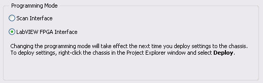
Hybrid mode requires you to have a bitfile compiled running on the FPGA to be able to read the Scan Interface IO Variables. Move the target FPGA at the RT target module will allow Interface of scanning for this module, but the frame will always mode Interface of LabVIEW FPGA.
To get fair access to the scan mode for the frame, right click on the chassis in the project, and choose Properties. Then, modify the Scan Interface programming. If you want to continue using the programming of FPGA and the Scan Interface set (hybrid mode), you will need to compile a bitfile (empty if you do not want programs on the FPGA again or containing your FPGA code). By compiling, the support of the module scan mode for the modules under your RT chassis is compiled in your custom bitfile. Then, on your VI RT, you need to use reference FPGA VI open to your newly compiled VI. Once this VI is deployed and ongoing implementation, you get the data from you are the CIE.
For more information, see this knowledge base article and Reference Interface of Scan CompactRIO and procedures.
-
How to check the instance datafile I/O? solve the high physical reads/writes?
Method-1
identify 'hot spots' or I/O contention
Select NAME,
"Physical reads," PHYRDS
round ((PHYRDS/PD.)) (PHYS_READS) * 100, 2) «Read %»,
PHYWRTS "physical Scriptures."
Round (PHYWRTS * 100/PD.) PHYS_WRTS, 2) "% of writing."
FS. PHYBLKRD + FS. PHYBLKWRT "Total block I / O of.
de)
Select sum (PHYRDS) PHYS_READS,
Sum (PHYWRTS) PHYS_WRTS
v $ filestat
) pd,.
v$ datafile df,.
v$ filestat fs
where df. FILE # = fs. FILE NO.
ranking by fs. PHYBLKRD + fs. PHYBLKWRT / / desc
Another method-
On Oracle10g, CWA also provides the dba_hist_filestatxs table to track the disk i/o:
break on begin_interval_time jump 2
column phyrds 999 999 999 format
column begin_interval_time format a25
Select
begin_interval_time,
file name,
phyrds
Of
dba_hist_filestatxs
natural join
dba_hist_snapshot;
It is - method that you use to check for errors in data I/O file? AND how to solve high physical reads and writes?Ankit Ashok Aggarwal wrote:
AWR project stat e/s in terms of segments, query and etc.
Here, my concern is what should be the value of ideal threashold for a DBA to act on the high physical reads/writes?
and how he can fix this problem if it affects database performance?I don't think that there is any possibility to mention that the amount of an e/s is going to be good or bad for a database in general. The reason is that it is not quantifiable. For example, in a store, maybe one day that no one gets and another day, there is no place to stand (because there was a sale announced by the store). So now, how do you say that it was not necessary? Rather than search for best practice values, it is best that you keep track of the normal functioning of your db and when you see a special summit in the values of events scattered user IO as DB file read, DB file parallel read etc and when this happens, you should check back the work you are doing and see if that can be refined somehow.
Aman...
-
How do you know the speed of read/write of a flash drive?
Who knows a program to read/write speed?
Hi Cristi,
Thanks for posting in the Microsoft Community.
An indication of the standard flash drives read/write speeds is the following:
USB 2.0:
Sequential write speed range = 4-10 MB/S
Sequential read speed range = 15 to 25 MB/S
USB 3.0:
Sequential write speed range = upto20 MB/S
Sequential read speed range = upto45 MB/S
These reading and writing speeds offer a guide to the read/write Flash Drive performance and have been identified in recent tests. Please note that we are changing the components USB Flash Drive at any time based on the availability and cost. This means that the read/write speeds above cannot be guaranteed.
You can use your favorite search engine to search for this application that measures the speed of read/write of flash drives.
Warning: Using third-party software, including hardware drivers can cause serious problems that may prevent your computer from starting properly. Microsoft cannot guarantee that problems resulting from the use of third-party software can be solved. Software using third party is at your own risk.
Hope this information helps. For any other corresponding Windows help, do not hesitate to contact us and we will be happy to help you.
-
Problem with the digital data to write VISA function
I have a GE's PowerPC that is running on the VxWorks operating system. I have a tornado application where I run my C code to generate a file .o & .out, then I empty image .o files & .out for PowerPC via FTP, now I need to communicate with PowerPC of LabVIEW (via serial communication using VISA vi) using the VxWorks controls. When I enter orders VxWorks in LabVIEW
That is to say for Eg: 1 > ls --> the contents of a directory list IE .o & .out files. The problem I'm facing here is, when I run the vi, I am able to read the file in the box to read the string but keep files on speeding up juice,
2 > ld <> --> load a module object in memory. I face the same problem here.
3 > then I need to type the name of funtion main c program, after which I can give input to the program.
4 > I need to enter numeric data as inputs to my program. but the write VISA function accepts the only input string and read VISA function gives only out of string... I want to give digital entries and read the digital output. Any help would be appreciated.
Hi Luke,.
You can try with this reliable hyperterminal VI.
-
Someone at - it an example of LabVIEW for I2C communication to read/write an eeprom?
I use sbRIO-9636 with FPGA.
I already tried with the "Advanced I2C" example, but it works...
Can someone help me?
Another suggestion:
You know about the VI package manager? There, you can install an application open source I2C & SPI API (worms. 3.0.0.22). It is an easy way to implement a system of Bus I2C on an FPGA target.
In this way is a little bit smarter.
Maybe you like it.
-
Number of cycles in the target FPGA VI
Hello to everyone.
I'm working on a project where I use sb RIO 9636. I subtract a number of past and present of the encoder pulses. Here, I have attached VI that I use as target VI. When I use simulated I/O lets say that the program works correctly. When I compile VI on sbRIO I noticed that the LED indicator named x = y? never flashes (even if she flashes simulation). Also, when I put indicaton on the number of cycles of control, counting starts from a few very very valuable.
Could someone help me?
Thanks in advance.
Hi Chupka993,
I suspect that part of the behavior of the that you describe, is that when you change the clock of the loop, you change the speed at which the loop works. As GerdW said, this loop timer setting gives your code a rate at which it should run. For example, defining 1ms means that your code inside this loop executes once per millisecond, or 1000 Hz. ticks would work similarly, but I think the timescale ticks of the FPGA clock which is generally 40 MHz on our devices.
When you have the timer set to 1 millisecond loop, the code in the loop executes 1,000 times per second, and your iteration count would be 1000 times before update output, which means that your code runs a full 1000 iterations once per second. If you change the clock of the loop of 2 milliseconds, the loop will run 500 times a second sense that your 1000 iterations would take 2 seconds to run. I think that the behavior you're seeing is because the iterations are produce faster that you intend.
You need to understand exactly how much time it should take your loop to run 1000 times and then set the timer loop to the appropriate value to achieve this goal.
-
Problem with the series of read/write
Hi all
I don't know if this belongs here or on one of the guidance material, but I thought I would start here.
I have two devices which I am currently trying to contact via the serial ports on a PXI chassis in real time. In both cases, I series of software that seems to work fine when I use the serial port on the controller (for example, COM1). Now, I have two cards that I used two different systems to talk to these devices - 8430/2 and 8430/4. In both cases, when I use these cards, it seems I have periodic in response by devices delays when you use the same code that I use when talking through the serial port of the controller (i.e., I get some downtime when trying to read code error-1073807339). I tried to Exchange cards with spare parts, but I have the same problem. I can handle the delays to retransmit the command, but this destroys ultimately the determinism of the system given that the delay may create a pause of up to 2 seconds. I tried to change the size of the buffer, but I seem to have the same problem. Does anyone have any ideas as to what could happen?
Cheers, Matt
Thank you, Luis. Indeed, one of the errors being thrown was a timeout error (the other was thrown by one of the devices indicating that he did not understand the command sent). However, the problem wasn't that I was getting a timeout, but rather that I was getting an error on one platform and not on another. But it seems that I solved my problem - I simply set the I/O VISA Write mode to synchronous and this seemed to solve the problem I had.
Cheers, Matt
-
date and time of transfer to the target fpga
Hello world
Can I transfer the date and time of real time on target fpga in a sbRIO?
Thank you
Hello
You don't know why you would want to try this, can you clarify? You cannot send the timestamp as it is, but according to what you want to do, there will be a solution. This describes how a timestamp is stored in LabVIEW, but you probably want to send/receive something more easy to handle on FPGA.
Michael.
-
Hello folk of LabVIEW FPGA,
I have a project on target FPGA X, and I ran out of resources.
I want to recompile it on Y to the target to see if I'll be better off.
I saw this article
http://www.NI.com/white-paper/5075/en/
What explains the steps required at the port of the target of the target.
But in my case, I have multiple FIFO and registers said... I really wouldn't go well the process of re - declare them again, not manually, this could be source of errors.
Please see screenshot for clarification on what I mean.
So, is there advice, what a FPGA gurus you can give me to help out me?
Is there a way that I could copy a section of the LV Proj XML or somethig so that I don't have to report again to the hand like a robot?
Thank you
Maciej
so Bravo goes to a colleague of mine.
What you can do is select all the elements (of the FIFO and registers) you want to copy.
Go to the menu of LV Edit-> copy.
and then go to the LV menu in the new project, select the place you want to stick to the and then edit-> paste.

-
Reduce read/write SPI function 5bits.
Hello
I got a project to develop an SPI interface with 7 bits of address with a bit in mode (R/W), but records of test being only 5 bits wide. Is there a way to get the Subvi interface USB - 8451 SPI limit the number of bits in the data stream? Or you can release the chip, select so that only 5 bits are sent. If anyone has had some experience with it please let me know if this is possible.
Gary Tyrna
ggaryt wrote:
Thank you for your answer to my question. Unfortunately I can not bit-bang because of the operating speed of 50 MHz.Well, it's just a little one important fact.

NOR has only 1 SPI devices. I'm not aware of the third SPI devices that can operate at this speed, not to mention control the number of clocks.
I know not all this with the FPGA, but the basis for the LabVIEW FPGA Module specification is a 40 MHz loop rates. You may need to look at some digital devices at high speed that sells some OR. My suggestion is to contact your local sales representative OR.
Maybe you are looking for
-
How to change your password in thunderbird email - NOT the master password
I went to my service provider internet and changed my e-mail password. However Thunderbird does not accept my changed password. I don't HAVE a "master" password Help. [email protected]
-
Significant improvements to a Thinkpad R61e, advice needed
I will try soon to upgrade a laptop Home Basic edition of Windows Vista 32 bit (7649-CTO). The end result, I hope, will be:(1) Microsoft Windows 7 Home Premium 64 bit install disk(2) used Intel X - 25 M 160 GB SSDSA2M160G2GC 2.5 "SSD Solid State Hard
-
I bought a laptop HP G6 - 2201 AX on October 31, 2012, and I got to know that by sending a request for project of rs. 2499, I can get a camera Nikon coolpix... My redemption code: 5361394 and product serial number: 5 CD 2376060 and product number: C
-
How can I send a resume by e-mail
I did a summary in microsoft word and would like to send to my email to send it to the employers by e-mail how can I do?
-
I did the initial installation on a computer and put the wrong name in. How can I change now?
There is a locked system titled "Jennifer" folder which should be called the "Moca".