PCI-7813R field
Hi, I use a PCI-7813R and cards PCI-6225 and I would check if the MASS D, GND AI and AO GND are connected to the chassis/building land. Thank you.
Hi Napoy,
For cards, AIGND, AOGND and DGND, all are connected internally to the chassis ground (which, if plugged into a properly wired outlet is connected to a building plot).
This is confirmed in these two articles:
How are the various related grounds in an R Series device?
http://digital.NI.com/public.nsf/allkb/1670D0423F6A123E862576EB0070D63F?OpenDocument
Are the ground on my DAQ devices all tied together?
http://digital.NI.com/public.nsf/allkb/02A451C0A88A3EAE8625702F0059C98E
Tags: NI Software
Similar Questions
-
Windows 7 64-bit PCI-7813R compatibility & PCI6225 cards.
We have a desktop PC that works under Windows 7 (64-bit). Labview 2012 64-bit version is compatible with
PCI-7813R & maps PCI-6225?
There is no 64-bit versions of the FPGA or RT modules at this time. The interface LabVIEW FPGA host does support 64-bit, but it's just to interface with the target once a bitfile has been deployed and does not allow you to create a new 64-bit LabVIEW bitfiles.
So, if you are doing development on this machine, you must use the 32-bit version of LabVIEW (works great, even on x 64 OSes). Your hardware all still work no matter what. I just wanted to be clear that for development, you should use the 32-bit version of LabVIEW when working with modules FPGA or RT.
-
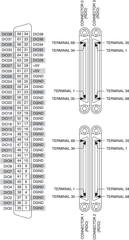
Nominal current PCI-7813R 5V Terminal
What is the maximum load for the terminal 5V on the connector 0 of the PCI-7813R card? What is the amperage of the fuse of the Council?
Yes, this A 0.5 limit applies to pins 27/28 (+ 5V) connector 0 on the PXI-7813R system.
-
What are the options for 3 bit for Hw_Arm_Sel in PCI-6601 field
Hello
I'm programming our own driver to operate the PCI-6601. For our application, we need option arms material. I know, it is possible to use 2 counters for this, but NEITHER-TIO also supports hw_arm. Although it is not explained in the registration document at all, after some tedious verification in the DDK examples I found that the pieces are in the Gi register metering mode. I know that the position of the HW_enable as well as the position of the 3 options sellect bits PIN. What I don't know is what are the options of 3 bits for Hw_Arm_Sel field. I contacted the support NEITHER, but received no support. How can NEITHER sell boards and when a customer who doesn't use LAbview or Measurement Studio, or DDK, but implements its own driver is then so arrogant at least of NOR? Also, how can OR publish only a part of the records of the Board of support and when a customer contacts and request for some records do not get supported at all? I can't predict the missing records, and he is professional enough to document comes in part from records of 660 x Instruments. And, upon request, you have nothing.
I hope that someone from the community are aware of this Hw_Arm_Sel 3 pin option. Otherwise, there is just one option of the error and the trial. Or simply throw away the jury.
Dr. Kirco Arsov
Hey, sory for the delay in my response. It works and it works very well with the description of Joe and Joe, thanks for your great help. I greatly appreciate. Now we finally also have this option as we wanted it and it works fine.
-
OR PCI-7813R is recognized as PCI-7811R
Thanks a lot for your help intend. I found the solution. It was the mistake in our laboratory. I used the wrong advice. It was really 7811 I had in my PC. Map right (7813) was on the set.

Life is funny, but sometimes we lose a lot of time and resources by mistake.
Thanks and greetings
Artur
This task should be now closed.
-
I have a question about a FPGA project I'm developing.
I use a digital RIO NI PCI-7813R, objective and Module FPGA 8.6.1
I implement a SPI bus, master.
I use a state machine in a single loop of Timed Cycle. (about model on one of your examples IP)
I'm running the loop at 20 MHz, which produced a clock of 10 MHz SPI bus data.
I send you the data in 8-bit bytes delivered by a FIFO of the host.
Similarly, I return data bytes of 8 bits of the host by using a different FIFO.
I have no problem sending data, generate all the select chip and data impulses on my desired clock edges.
It's manual clean and perfect as seen on a scope / Logic Analyzer.When I read data from i/o pin however I have found unexplained behavior.
It is this: the data seem to be trolling by two read operations.
When I read the axis of I/O data to the specified limit of the clock that I generate.
I found that the data were two bits shifted to the right, i.e., deferred, one on the scope / Logic Analyzer.
I did a work around by two pins I/O multiple read operations in time of the gap between the data bytes.
There are no generated clock signal and no data valid on the I/O pin at the time of these two read operations as testified to by the scope.
And now the data received matches perfectly to the one sent.
I can only assume that there is some kind of pipeline or delay inherent in the IO read operations. (at higher clock rates)I suspect that there may be something in the optimization performed in the compilation of the structure of the SCTL the cause.
I had found it, sometime before in my development, that data has been little offset from 1 only one position.
I think it was at a slower pace of global clock.I also ran the same state machine in a classic logic expect everything in a loop with an FPGA, to produce a much slower system
and I found that there is no delay at all.I don't see anything in the configuration i/o pins that can affect this. (I turned off arbitration)
Similarly, I don't see anything in the documentation that could refer to this behavior.
8.6.1 of LabVIEW FPGA Module Known Issues (http://digital.ni.com/public.nsf/allkb/F6B5DAFBC1A8A22D8625752F00611AFF)I'm about to use and deploy the code with the solution because it seems to be reliable.
But I am at a loss to explain (in my documentation of the code) why it is necessary
or how to solve this problem if the compiler changes.
Do you have any suggestions?I think that what you run is that the number of sync records used with the digital I/o. If you right-click on the I/O item in the project and select the property page, you should see an option for number of registers for output and output enable synchronization. These settings are global settings for this I/O item that will be the effect on all nodes of the I/O writes to this point of I/O. Similarly, if you right click on the e/s on the schema node and select Properties, you should see a setting for number of registers of synchronization for playback. This setting is specific to this instance of the node for this element of I/O and can be configured differently for each node in the diagram. The effect is that each sychnronization registry will delay this beating of a clock signal. These records are inserted to prevent the problems of metastability and ensure that you always have signal levels valid when the IO is sampled on the edge of the clock. There is a problem whenever the producer and the consumer of the signal are market off different clocks, or at different clock rates. If the external device drive your digital inputs work synchronous clock you are producing, you can eliminate the registers of the synchronization. However, you must perform an analysis of delays in propagation of the signal between the two devices and make sure that all the settings and hold times are always met before. In the end, I think that the easiest and most robust solution will be to compensate for delays in sync in your code as you do already. I hope this helps clarify things.
-
What slot PCI should I use to install the Wireless PCI card
I have a Compaq Presario CQ5210F desk top. I add a Sabrent PCI-G802-PCI-54Mbs, 802.11 wireless card g. I've read all the how info pages and am like that. The unit has 1 PCI Express x 16 & 2 PCI Express x 1 slots. Which slot is OK for this device and it is where or how can ensure me that I use housing appropriate?
None of how information talks about it and I don't want to play and FRY my computer.
You are the very welcome, and Hanspuppa is very modest.
It is indeed an expert in the field.

Paul
-
Problems of PCI-6224 entry entirely analog differential.
I use the 6224 Board of PCI of e/s and I have problems with the fully differential analog inputs. I have the pins connected to a power supply in order to test their functionality. The test of negative tensions, it works perfectly. All testing positive tensions when the test voltage is greater than approximately 5V results there is real tension about 10V breaks several times. On land, it looks like a square wave. Anyone know what would cause this?
You have the polarization resistors on the + / lines? Looks like you're floating out of the common-mode range. The guide of field wiring. http://www.NI.com/white-paper/3344/en
-
Hi, I would ask for some help to get a better understanding of the works of the FPGA. I use PCI-7833R. As the field programmable gate array, each time I want to launch a new FPGA vi, without using the emulation, the program is compiled in the table. This means that some part of the Bay door is irreversibly programmed? For PCI-7833R, how many times can I compile my FPGA vi on the motherboard? How much space does have? It would happen the whole picture card is programmed and I can't use the card again? Thank you very much! I appreciate any help or information. Any reference or basic documents would be much appreciated as well.
soljiang:
The FPGA is fully reconfigurable, so if you place a new VI FPGA on your 7833R, crash just any previous configuration and it won't run out of space. The FPGA programming is NOT irreversible, so don't feel bad if you need to change your VI and recompile; prototyping, as this is precisely what the Board is designed for.
The 7833R a Virtex-II FPGA, then wear it hs 3 million (see tables in the following items or the page of the product here).
If you are looking for basic documents, here are a few good ones on the NI Developer Zone.
-
How to make your own Board BNC connector for 37 pins PCI-6010?
This is first time I am doing data acquisition and the BNC-2110 present can be connected to PCI-6010. How to make a Board for it?
I'm not sure what you mean by "some"; The BNC-2120 exposes all channels HAVE and AO on connector 0 of a standard feature of E, M or X series.
- Eight BNC connectors are for eight differential channels of I. For example, for the BNC connector labeled 'I 0', the Center connects to the 'I 0' pine and the outside connects to pin 'HAVE 8'. (The BNC-2120 probably would not be a good choice for someone who wanted to use the channels in unbalanced mode).
- Other two is for the analog output; the centres are ' AO 0' and 'AO 1' and transmissions are related to "AO GND".
- There is another connector BNC for PFI 0; all other PFI (with the exception of the 10, 11 and 15) are broken down as screw terminals.
- Other BNC connectors connect what either directly (the unit is powered by the + 5V line but otherwise works autonomously, and the "user defined signals' are connected to terminals to adjacent screws).
It seems like it wouldn't be difficult to have a cable that was going on a PCI-6010 the 37 pins on the connector 68 pins on the BNC-2120. I'm a little curious as to why we do not have one. Possible reasons off the top of my head which may explain why not:
- cards PFI/description would be a mistake (for example, on a series of E/M/X ' CTR 0 SRC "PFI 8; on the 6010 is PFI 0.)
- No digital lines (E/M/x series P0.0 P0.7 via are independent; on the P0.0 6010 P0.5 and P1.0 by P1.3 are shared with PFI lines)
- Confusion about being able to connect to other devices that we sell with connector d - SUB 37 pin, but who do not use a compatible pinout (for example, the PCI-6239, PCI-6510 or the NI 9237). Here again, a PCI-6703 also uses a 68 connector pins, but has a completely incompatible pinout as well.
But it seems that those who would be pretty easy to deal with, because it is useful to be able to connect to the BNC-2010. Maybe it's an idea for the Exchange of ideas information Acquisition?
Anyway, if you want to have pushed BNC for everything on your Board of homebrew will need you:
- 8 or 16 BNC connectors to HAVE, depending on whether you want single-ended or differential. For differential, the centres are GOT by AI 7 0, and transmissions are AI by AI 15 8. For asymmetric, the centres are HAVE 0 through 15 AI and transmissions should all connect to GND AI.
- HAVE a sense (I think that you only need this if you use channels Nonreferenced Single - Ended (NRSE). See also: noise considerations for analog signals and field wiring.)
- Two for AO (centers are AO 0 and 1 AO, outers times connect to AO GND).
- Ten for PFI/digital lines. Outers will connect to GND D.
Up to a maximum of 29. You want maybe less, depending on your application.
-
6225 PCI residual voltage in the analog input channel
Hello, I'm new to the Forum and just start working hands with NI hardware/software/etc.
I use MAX (differential setting) to monitor an input channel analog (ai71) through a PCI-6225 card with an SCB-68. The voltage displayed in this MAX sometimes regular 10.6 volts and sometimes intermittent noise 0 to 10.6 volts or vague angular. I watched the disintegration of noise and waves to zero. The voltage displayed in MAX is (seemingly at random) changes when a voltmeter is used to measure the voltage between pins 1 and 35 (with no wire signal)
When an external square wave (2.7 volts DC) is applied to the pins 1 and 35 in the SCB - 68 the value in MAX is dominated by the 0 - 10.6V 'noise', while a voltmeter between pins 1 and 35 simultaneously shows the square wave.
Any suggestions? Thank you in advance.
If you dig into the data acquisition specifications, input voltages must be referenced to the mass of AI or you may damage the Board. Have a good read of this article: wiring field and considerations of noise for analog signals. Since you're probably dealing with a differential signal with no mass, what you want to do is to add resistance on each side of the signal to ground. This article recommends until 100kOhm 10kOhm resistors.
-
I use pci-6221, I need her to interface with thermocouple with voltage up to 5v
I use as my pci-6221 or data acquisition card and card 8.2.this labview version gives the constant 10.5 volt signal in at the entrance to analog channel AO on pin 68 and 34. why it shows 10.5 although I did not connect any input.i use type k thermocouple and after signal conditioning with tl0804 I need it interface with AI 0.i channel unaware aware of off the road on the output pins this Card.i need to operate an electric rod that needs 24 volt DC.i give entry to the pins HAVE with variable dc power block after reaching the limit I set(eg:2v) it jumps instantly to 10.5 volts.
You have your task to acquisition of data configured for the mode differential or asymmetric acquisition for the analog input?
I don't understand your comment about to connect the pins WITH a DC power supply. Why is that you connect a DC power supply to the analog input?
Using an analog output or digital output to operate the electric rod? I'll assume that you are looking for on/off control. A digital output is not the voltage or current to drive something that big. You may be able to find a relay for coil 5VDC. Check current requirements. With which you can have the relay to connect or disconnect a power supply of 24 VDC is the actuator. Make sure you have a protection diode across the relay coil wired, so that the magnetic field of the coil does not damage the analog output of your card.
Another possibility is to have the 5 VDC output transistor circuit switches the 24 VDC circuit.
-
PCI Ethernet card does no not after PCI slot
I have a card to PCI Ethernet D-Link DFE-520TX in one of the PCI slots and connected to a Linksys router.
I wanted to install a new sound card so I changed the Ethernet card to an adjacent PCI slot. (without uninstalling the Ethernet card)
After you install the sound card, I found that I am not able to connect to internet!
These are the observations I made:
The connection icon says "Limited or no connectivity."
When I click on icon of connection, status shows bytes sent/received something like that...
Bytes sent: 4536 Receieved: 0
The IP seems to be assigned by AutoIP.I tried to uninstall the Ethernet card drivers and install again for the new PCI slot but no luck

Finally, I gave up and restored the adapter Ethernet to its former PCI slot... and surprise, his does not work here too!
A I miss out on something?
Any help with this would be really appreciated. Thanks in advance.Hello
His work...
In fact the IP, DNS etc. had been configured manually.
When I removed the LAN card, all fields has scored zero, I wasn't expecting that to happen!
Thanks anyway!

-
Relatively easy PCI controller driver
Hello friends,
I have (3) DC5800 64 bit, CORE 2 DUO processor microtours I provided an image for windows OS 7 Enterprise. The only issue I'm having is with relatively easy PCI controller. The screen of the Device Manager under other devices States that PCI simple communication controllers are not installed. There is no manufacturing not listed in properties and the only other information I can provide are the place field States PCI bus), device 3, function 0. Due to the security setting I can't go to a website to update, I can only download drivers for an external hard drive and then update.
So my questions are:
- 1. how to identify drivers proper?
- 2. where are located the correct drivers?
Thank you all for the time and consideration in this way.
I downloaded the driver from Ty
-
I have a HP Envy 15 running Windows 7. I recently had the hard drive replaced and all the software reinstalled. I get error 28 for my PCI driver
. Any help?
You have added the necessary details which should help figure this point.
You can probably find the drivers you need in the community of HP, but we would need your model number to help find that (there are more than one HP Envy 15):
But once you used Device Manager to determine the properties of a device and can display the vendor and device numbers:
You can visit:
PCIDatabase.com
And plug the values in Device Manager when the seller is 10EC and the unit is 5209:
By clicking the search box on the device and match the results you says it's a Realtek PCIE card reader device kind:
By clicking on the name of the seller link will lead you to the Realtek page that allows to locate the 5209 device and get the link to the Realtek site, where you can search for drivers (in the Notes field):
And on the Realtek page, there is only one option in the page that refers to a card reader for Windows 7:
I think it should.
But, you might check the download page for support/HP also and see what they have to say.
This idea will work for any device in the Device Manager, as long as you can get the vendor and device ID.
Maybe you are looking for
-
something is running in the background on my phone, how can I stop it?
iPhone 6 has something to the background using battery
-
Firefox crashes when I move the mouse on the history tab in Firefox 7.0.1. Why?
Whenever I move the mouse over the menu history in firefox 7.0.1 program just hangs, I get a spinning wheel on Win 7, if I click on the program, it fades and becomes white. After about 20-30 seconds, everything goes back to normal, except that I can
-
Start thakes a minute
-
Simple question LED to a beginner.
I have two identical loops in series while. Each one as a clock and a light timer expired. When I run it, the first LED lights up, then the second LED. When I re - run, first LED reset and the second LED stays on. Once the first while loop ends,
-
(Redirected) Problems with Customer Service
Dell didn't ship my computer as shown in the command. I had to call and send a mail to get it shipped. Shipping on the order, which has affected the guarantee date then no corrected. I can't seem to get anyone to understand that. (A couple of other q