Sub - VI implicit calendar within a LabVIEW FPGA SCTL
I have a question about the time of a Subvi in one SCTL when LabVIEW is translated into VHDL. Did the translate Flatten all code within the SCTL effectively remove the Subvi borders, or a Subvi act like a framework unique sequence around this code.
For example, if I have a block of code inside a Subvi, which is not connected to any entrance or exit of the Subvi, is it still wait for all entries of Subvi settle for run? I know that the answer is Yes normally, but I was wondering if it was different inside a SCTL. If the answer is always Yes, remove implicit synchronization in the construction specifications FPGA effectively remove this application for each block of code that is not directly connected?
I ask because sometimes I wonder if the code inside a Subvi, which is part of the critical path of a loop may be simplifying the BD, but can be the critical path timing wrong because some functions/gates do not run as soon as they can if it is inside a Subvi.
The SCTL flattens all code inside, by removing all intermediate registers.
So Yes use Subvi to cleanup code / duplicate inside SCTLs.
Tags: NI Software
Similar Questions
-
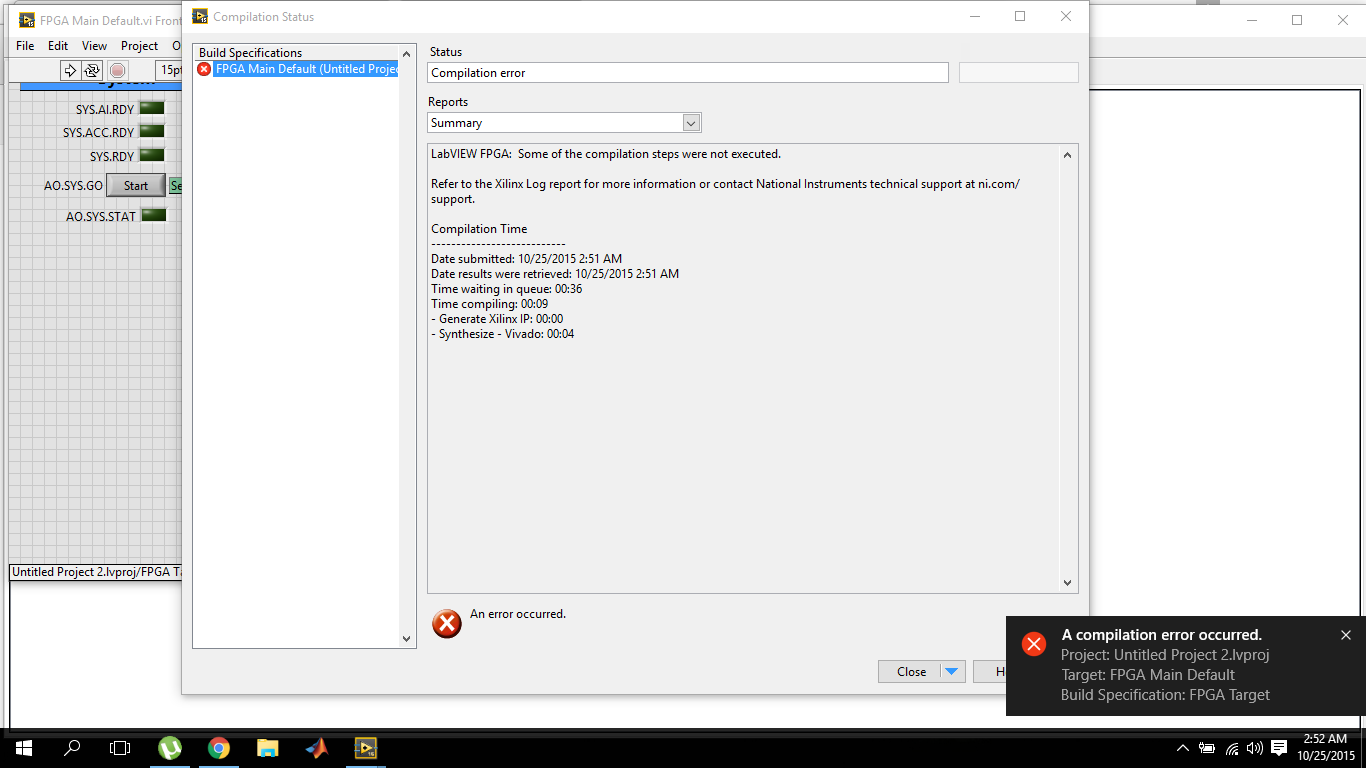
LabVIEW FPGA, 2015 compilation error
I've recently switched to LabVIEW 2015 and I'm working on OR myRIO. So also installed myRIO 2015 bundled software. The problem I have is that the compilation of fpga fails within 10 seconds.
and the target Xilinx journal report is empty
The first time when I tried to compile on 2015 version, it failed and the message box that failed came alongwith the avast antivirus warning for malicious activity. I reported it as wrong and now I tried several times with avast shield disabled control, but the results are the same. While the version of labVIEW 2014 works very well.
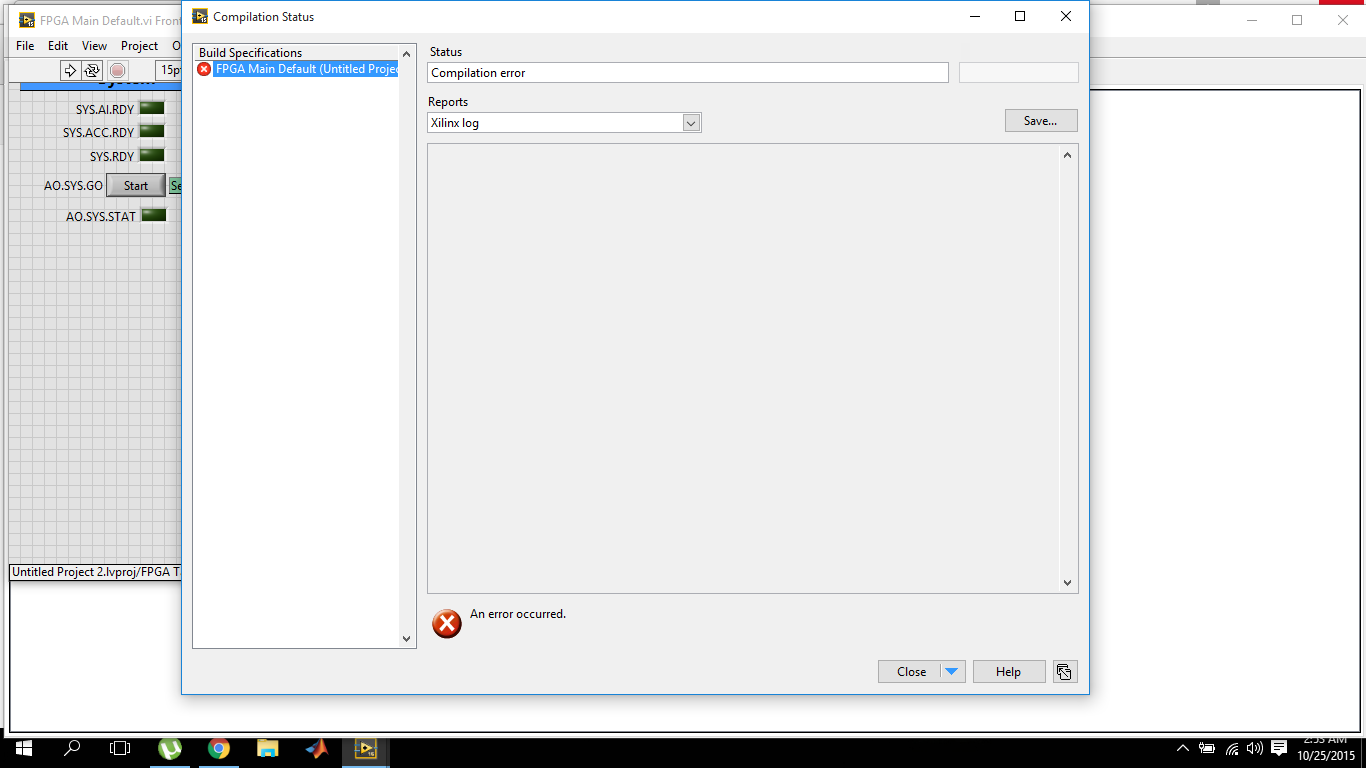
Now, I'm sure that there is something wrong with the installation of Vivado because this dll is part of it. The dll must be default in the2014_4\lib\win32.o directory C:\NIFPGA\programs\Vivado if you are using an operating system for 32-bit AND also in C:\NIFPGA\programs\Vivado2014_4\lib\win64.o If you use a 64-bit operating system. If the dll is not here, it is probably that the anti virus (I've never seen what happens to Xilinx but I have for other stuff).
I'm emphasizing the 2014_4 because LabVIEW 2015 uses Vivado 2014_4 while 2014 LabVIEW uses Vivado 2013_4. Since you have also installed LabVIEW 2014, you must have 2013_4 as well and if it works, you will find the dll I just wanted you make sure you check the correct directory for the Vivado 2014_4.
Download and install (reinstall or repair if already installed) 2015 LabVIEW FPGA Module Xilinx tools Vivado 2014.4. You can also use the DVD Setup if you have. It would be a good idea to do the installation with the disabled and even anti-virus try the first compilation the same. Try and let me know if the problem persists.
Kind regards
-
How to measure the frequency of sampling (s/s) in LabView FPGA?
Hello
I am trying to find a way to measure the sampling frequency (s/s) during which I read from analog input in LabVIEW FPGA. I know that the sampling frequency is specified in the data sheet of the module HAVE, but I want to measure in LabVIEW.
Any suggestions?
A screenshot of the example code would be greatly appreciated
Hey phg,.
If you have some time loopand in this loop, you export a sample by iteration of loop via an I/O node. You can't out two samples on the same I/O node within an iteration, it's always one!
So if your loop takes 1 second to run you have a sampling rate of 1 Hz output. The same goes for sampling of entry. How long your loop takes to run can be calculated as explained above.
Samplerate [s / s] = 1 / [s] while loop
-
LabVIEW FPGA CLIP node compilation error
Hello NO,.
I work on an application for my Single-Board RIO (sbRIO-9601) and faced with a compile error when I try to compile my FPGA personality via the ELEMENT node. I have two .vhd files that I declare in my .xml file and all at this point works great. I add the IP-level component to my project and then drag it to the VI I created under my FPGA.
Within the FPGA personality, I essentially have to add some constants on the indicators and entries CLIP to my CLIP out and attempt to save/compile. With this simple configuration, I met a compilation error (ERROR: MapLib:820 - symbol LUT4... see report filling for details on which signals were cut). If I go back to my VI and delete indicators on the output (making the output pin of the CLIP connected to nothing), compiles fine.
I've included screenshots, VHDL and LV project files. What could be causing an indicator of the output of my VI to force compilation errors?
Otherwise that it is attached to the output ELEMENT, a successful compilation...
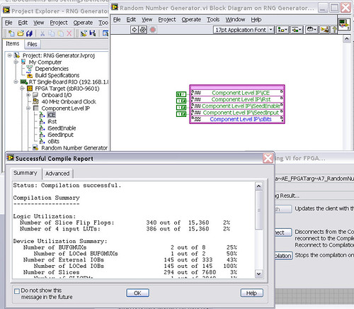
After that the output indicator comes with CLIP, compilation to fail...

NEITHER sbRIO-9601
LabVIEW 8.6.0
LabVIEW FPGA
Windows XP (32-bit, English)
No conflicting background process (not Google desktop, etc.).Usually a "trimming" error gives to think that there are a few missing IP. Often, a CLIP source file is missing or the path specified in the XML file is incorrect.
In your case I believe that there is an error in the XML declaration:
1.0
RandomNumberGenerator
urng_n11213_w36dp_t4_p89.vhd
fifo2.vhd
This indicates LV FPGA to expect a higher level entity called "RandomNumberGenerator" defined in one of two VHDL files. However, I couldn't see this entity in one of two files. If urng_n11213_w36dp_t4_p89 is the top-level entity, edit the XML to instead set the HDLName tag as follows:
urng_n11213_w36dp_t4_p89 Also - in your XML, you set the 'oBits' music VIDEO for output as a U32, however the VHDL port is defined as a vector of bits 89:
oBits: out std_logic_vector (89-1 downto 0)
These definitions must match and the maximum size of the vector CLIP IO is 32, so you have to break your oBits in three exits U32 output. I have added the ports and changed your logic of assignment as follows:
oBits1(31 downto 0)<= srcs(31="" downto="">
oBits2(31 downto 0)<= srcs(63="" downto="">
oBits3(31 downto 0)<= "0000000"="" &="" srcs(88="" downto="">Both of these changes resulted in a successful compilation.
Note: The only compiler errors when you add the flag because otherwise your CUTTING code is optimized design. If the IP is instantiated in a design, but nothing is connected to its output, it consumes all logic? Most of the time the FPGA compiler is smart enough to get it out.
-
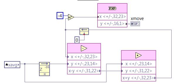
I created a Labview FPGA .vi using a structure flat sequence that shows the output of a sensor at a sampling frequency of 1 kHz on a digital SPI. After reading, I write the point data fixed in a FIFO, which is read by a host vi and finally written on the hard disk for post-processing. I need to add logic for the calculation of the average for the further process the signal FPGA vi. I want to continue at the exit of the original 1 kHz sampled datat to the FIFO, but also perform a sprawl on the steps and write these results at the same frequency of 1 kHz to the FIFO. The average feature, I would like to implement is a two-step process. Step 1 is to take samples of 1 kHz and perform an average of 16 samples based frame. In other words, I want samples of sum 16 1 kHz and dividing by 16 and decimate 16:1, which produces data of 62.5 Hz. Step 2 is to take 62.5 Hz sampled data and perform a moving average of 16 samples on these data and output resulting at the same sample rate of 62.5 Hz. I want these 62.5 Hz sampled data to be injected into the FIFA as well as the original data of 1 kHz sampled (unmodified) at the frequency of 1 kHz.
I've got step 1 work correctly using the block "mean, Variance, StdDev FPGA vi" with number of samples on 16. This block runs within a sequence of flat sequence structure after I received each sample 1 kHz on the SPI. My fight is the average feature mobile step 2. I try to use the code in the screenshot below, but am unclear regarding how/where to implement this logic inside is my structure flat separate sequence while loop, structure of the case, etc, in order to ensure that it only works on one of 62.5 Hz samples to this flow of data at once. I tried to put it inside the sequence that executes the block average and further in a case that is driven by the Boolean "valid" the average block output. I obviously don't understand how these different loops run, because it does not work properly. Can someone tell me how to implement the logic of moving average in my vi FPGA existing to produce the desired results as described above? Screenshot below of the logic (step 2) average mobile I am trying to use. In addition, find attached my screws vi FPGA that I need help with is 'CA215_SPI.vi' and the level vi host is 'Host.vi '. Thanks in advance.
Joel
This question is closed. I realized that my approach to implementation was actually working. I just had a stupid mistake on my fixed point output bit size, giving me results errenous.
-
Use of FIFO memory on two areas of clock (Labview FPGA) block
Greetings!
I'm developing an application on the FPGA of the vector signal OR 5644R
transmitter/receiver. I have two loops single-cycle timed: a 40 MHz making a convolution
and writing a FIFO memory block and the second at 120 MHz (sample clock)
who reads from block FIFO memory and uses the following values
interpolation...Under what circumstances is it permissible to use a FIFO memory block to transfer
values of a loop from 40 MHz to a loop of 120 MHz (sample clock)?
The reason I ask the question, it is that the compilation of my code repeatedly of not
reported the error below:ERROR: HDLCompiler:69 - "/ opt/apps/NIFPGA/jobs/J9k7Gwc_WXxzSVD/Interface.vhd" line 193:
is not declared. I share for everyone's reference, screenshots of my code which is an extension of
sample 'Project streaming VST' given in NI5644R. A brief description of attachments is
given below...
1. "Top_level_FPGA_part1_modification.png": in a loop SCTL 120 MHz, a sub - vi bed FPGA
go a block FIFO memory... In fact, the reading is actually made when entry
"read_stream" is activated... (see details in read_from_fifo_true_case.png)
2. "Top_level_FPGA_part2_modification.png": a 40 MHz SCTL, wherein is a subvi FPGA
called to write the output of convolution to block FIFO memory.
3. "target_respone_fpga_block_FIFO_modification.png": an output of a convolution filter is
written in block FIFO memory each time that the convolution output is available...
'ReadBlockFIFO' VI (circled in Top_level_FPGA_part1) is invoked in a 120 MHz SCTL.
4. "read_from_fifo_false_case.png": when the input "read_stream' of this vi is false,
data transfer memory FIFO of block to a different FIFO ('generation filter") takes
place.
5. "read_from_fifo_true_case.png": when the "read_stream' is set to true, the data is read in
'Filter generation' FIFO and spent on the chain of later interpolation to the
120 MHz SCTL...
I hope that the attachments give enough clarity to what I'm doing... If we need
For more information, do not hesitate to ask...
Kind regards
S. Raja Kumar
Greetings!
I think I understand the problem... The error probably occurs because a DMA FIFO
(FPGA host) is playing at 40 MHz, and it is checked for the number of items in a loop
120 MHz... It is not captured by the "pre-processing" by the labview FPGA, but by the Xilinx
compilation phase synthesis tool.
A lesson I share, is that if you observe this kind of problem, watch if there is incompatibility
in the areas of the clock to access a FIFO...
Kind regards
S. Raja Kumar
-
Integration of IP node evil in LabVIEW FPGA
Hi all
I am having trouble with the integration of LabVIEW FPGA IP option and was hoping someone could shed some light here.
I use a simple VHDL code for a bit, 2: 1 MUX in order to familiarize themselves with the integration of IP for the LabVIEW FPGA.
In the IP properties of the context node, the syntax checking integration says:
ERROR: HDLParsers:813 - "C:/NIFPGA/iptemp/ipin482231194540D2B0CC68A8AF0F43AAED/TwoToOneOneBitMux.vhd", line 15. Enumerated value U is absent from the selection.
but I'm still able to compile. Once the node is made and connected, I get the arrow to run the VI but when I do, I get a build errors in Code Pop up that says:
The selected object is only supported inside the single-cycle Timed loop.
Place a single cycle timed loop around the object.
The selected object in question is my IP integration node.
I add a loop timed to the node, but even if I am able to run the VI, it nothing happens. the output does not illuminate regardless of the configuration.
I would say that I tried everything, but I can't imagine would be the problem might be at this point given that everything compiles and the code is so simple.
I have attached the VI both VHDL code. Please let me know if any problems occur following different boards of the FPGA.
Would be really grateful for the help,
Yusif Nurizade
Hey, Yusif,.
Looks that you enter in the loop timed Cycle and never, leave while the indicator of Output never actually is updated. Try a real constant of wiring to the break of the SCTL condition. Otherwise, you could spend all controls/indicators inside the SCTL and get rid of the outside while loop. You can race in the calendar of meeting bad in larger designs without pipeling or by optimizing the code if you take this approach, however.
-
CPU register accessible in LabView FPGA FlexRIO
Hello people, I wonder if it is possible to get the following behaviors of Labview. I think that it is not.
Description of the system: application of CVI which communicates with SMU FlexRIO via controls and indicators.
Problem: The design of a CPU-FPGA interface specification which lists the "books" as a combination of reading and reading/writing-the bit fields.
Example:
According to the specification, there should be a 32-bit register. 31: 16 bits are read-only, and 15:0 bits are read/write, from the perspective of the CPU. In the world of labview, I would just do a uint16 control and indicator of uint16 and do with it.
However, to meet the specification (written for microprocessor buses) traditional, a reading of 32 bits of an address should read back the full content of the 32-bitregister to this place (implemented as flops on the FPGA, with appropriate memory within the FPGA device mapping). In the same way a 32 bits of an address entry must store the values in this registry (properly masking wrote at 31: 16 bits within the FPGA device).
Is it possible for me to have a unique address (basically, a component unique labview block diagram) that will allow me to accomplish this behavior? It seems to me that the only solution is to pack my records with bit fields that are all read, or all the read-write in order to register in the paradigm of labview. This means that the spec should go back and be re-written and approved again.
Thanks in advance,
-J
Thanks for the detailed explanation. I am familiar with the reading and writing in the FPGA registers - I did a lot of work non-LabVIEW recently with an Altera FPGA. I haven't, however, used the CVI to LabVIEW FPGA interface, I only used the LabVIEW interface. I'm not sure if your question is about the CVI, LabVIEW FPGA interface or both.
JJMontante wrote:
Thus, a restatement of my original question: y at - it a mechanism with the use of indicators of controls where both the FPGA AND the CPU can write to the same series of flip-flops in the FPGA? If I use an indicator, the FPGA can write to the indicator, but the CPU cannot. If I use a control, the CPU can write in the control, but can't the FPGA. Is this correct?
On LabVIEW FPGA, a control and indicator are essentially identical. You can write a check, or read a battery / battery, using a local variable in the FPGA code. It is common to use a single piece of front panel to transfer the data in either sense, and it's okay if it's a command or an indicator. For example, a common strategy uses a Boolean façade element for handshake. The CPU writes a value to a numeric control, and then sets the value Boolean true to indicate that the new data is available. FPGA reads this numerical value, and then sets the Boolean false, which indicates the processor that the value has been read. The LabVIEW FPGA interface (side CPU) covers also all elements of frontage on the same FPGA whether orders or the lights--they can be as well read and written.
That answer your question at all?
-
Simulate the sine wave using LabVIEW FPGA with NOR-myRIO and display in real time
Hello
I'm relatively new to LabVIEW FPGA. I am trying to test (and later apply) controllers high speed on myRIO.
At this point, I'm trying to simulate the sine wave from 1 to 10 kHz using Sinewave generator VI express. I also intend to display the sine wave on the time real (RT) using FIFO. However, I had a bit of trouble to understaing various synchronization parameters.
1. how to encode information about the sampling frequency generating sine wave? (The side FPGA vi requires only the frequency of the signal and possibly phase and does not rate update lines)
2. how to estimate the number of items in a FIFO? (that is, the relationship between the rate of updates to loop (RT), the signal frequency, sampling frequency and the number of items in the FIFO)
It would be great if we could share a very simple program (side host and target) that did something similar.
Thank you
MILIN
Milot,
I think the problem is the type of data in your FIFO. Your FIFO is configured to use a data type of I16. The problem is the number, it displays only ever will be-1, 0 or 1. To resolve this problem, you must send the sine wave as a fixed point data and convert it to a double on the side of the RT. This should significantly improve your resolution.
-
Internal software error of LabVIEW FPGA Module - 61499
I get the error next (in a pop-up window) in the phase of sompilation for the FPGA target with a vhdl IP. This error continues to occur even after restart LabVIEW and the PC. Someone at - it solved is this kind of problem before without having to re - install the software?
Here is the error information:
Error-61499 occurred at niFpgaXml_GetValue_String.vi<><><><>
Possible reasons:
LabVIEW FPGA: An internal software error in the LabVIEW FPGA Module has occurred. Please contact National Instruments technical support on ni.com/support.
Additional information: lack the tag required XML (/ CompileServerList)
As a first step, I can compile the vhdl IP node successfully. However, once when I'm running a VI with the FPGA, the bureau stop working. After that I restarted by force, it cannot perform the build of a vhdl IP node. Even without connecing to the jury of LabView, he pointed out errors before the end of the sompilation.
Interestingly, the screw which also includes nodes IP vhdl that I properly compiled before, I can still run the VI to the Commission and it works correctly.
Thank you
Looks like your ActiveJobsList somehow has been corrupted. I saw occur when computers are hard stop or blue screen during compilation. I don't have that LabVIEW 2014 installed on my machine, so your path will be a little different, and the file extension will be a .txt or .xml instead of .json, but try this:
Move the file "C:\Program Files (x 86) \National Instruments\LabVIEW 2014\vi.lib\rvi\CDR\niFpgaActiveJobList.json" (or your equivalent) out of the above directory (back it upward and delete essentially) and restart LabVIEW. Must regenerate the file and resolve the problem.
-
How to use bidirectional I/O in the CLIP of LabVIEW FPGA?
How to use or define two-way i/o for CLIP with LabVIEW FPGA? I want to use 1-wire communication inside the kernel CLIP, the function will be implemented to read and write as I/O inside the CLAMP.
The XML Generator (CXG) 1.1.0 ELEMENT does not support.
Thank you
Supawat
Work after separate IB pin (bidirectional) at the entrance and exit. Thank you.
-
NEITHER 9512 with Labview FPGA Interface
Is it possible to use the NI 9512 stepper with Labview FPGA interface drive unit or is it only possible to use it with the interface of scanning? When I try to add the module to a FPGA target, I get an error telling me that Labview FPGA does not support this module with the latest version of NOR-RIO, but I have the latest version of OR-installed RIO.
Hi Checkit,
You're right - the 9512 cannot currently be used in FPGA. There is an error in the documentation. The 9514 and 9516 can, however.
-
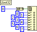
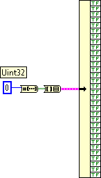
Int split into pieces in LabVIEW FPGA
Is there a clever way to split a Uint32 in 32 bit directly accessible (not a prison guard) in LabVIEW FPGA?
The only way I could come up with is the following, which is a writing of pain for 32 bit and seems a waste resources og to store all these clues.
.
Best regards, mola
I thought about it. I could use clusters by right-clicking on the table to the Cluster block and increase the cluster size in 32.
-
LabVIEW FPGA: Integration node clock wrong
Hello
I'm having some difficulties to understand how the clock is part of the node IP for LabVIEW FPGA and was hoping to get some advice.
What I try to do is to set up a digital logic circuit with a MUX feeding a parallel 8-bit shift register. I created the schema for this Xilinx ISE 12.4, put in place and can't seem to import the HDL code into an intellectual property node. When I run the VI, I am able to choose between the two entries for the MUX, load the output in the shift register, clearly the shift register and activate the CE.
My problem is that when I switch to the entrance of THIS, he should start 1 sec shift (Boolean true, SCR, High, what-have-you) in the registry once each clock period. Unfortunately, it instantly makes all 8 bits 1 s. I suspect it's a question of clock and here are some of the things I've tried:
-Specify the input clock while going through the process of configuring IP nodes.
-Adding an FPGA clock Constant as the timed loop.
-Remove the timed loop and just specifying the clock input (I'm not able to run the VI that I get an error that calls for a timed loop)
-Do not specify the clock to enter the Configuration of the IP node and wiring of the FPGA clock Constant to the clock input (I can't because the entry is generated as a Boolean).
-Remove an earlier version of the EC who had two entries up to a door and at ISE.
-Specify the CE in the process Configuration of the IP nodes.
-Not specify this in the process of setting up nodes IP and wiring it sperately.
-Various reconfigurations of the same thing that I don't remember.
I think I'm doing something wrong with the clock, and that's the problem I have. Previously, when I asked questions to the Board of Directors on the importation of ISE code in LabVIEW FPGA, a clock signal is not necessary and they advised me to just use a timed loop. Now, I need to use it but am unable to find an explanation online, as it is a node of intellectual property.
Any advice would be greatly appreciated, I'm working on a project that will require an understanding how to operate clocks the crux of intellectual property.
Thanks in advance,
Yusif Nurizade
P.S. I have attached my schematic ISE and the LabVIEW project with one of the incarnations of the VI. The site allow me to add as an attachment .vhd file, but if it would help I could just paste the body of the code VDHL so just let me know.
Hello Françoise,.
I spoke to the engineer OR this topic and it seems that it was sufficient to verify that your code works, by putting a wait function of 500 ms on the while loop to check that the registers responsible and clear. I'm glad that it worked very well!
-
Move from LabVIEW FPGA block of ram address to node CLIP?
Hello
I need to pass an index memory RAM of LabVIEW FPGA block to a CLIP node to the node CLIP to have access to the data in the BRAM. The node of the ELEMENT contains an IP address that we developed and the IP address is the use of Xilinx BRAM driver to access data. I guess that we need to move the physical address of the BRAM to the ELEMENT node.
Is this possible? If so, how? If this is not the case, what would be an alternative?
Thank you
Michel
If I understand you correctly, Yes, you should be able to use the memory block of the Xilinx pallet Builder in LabVIEW FPGA and in the loop of the single Cycle, connect the ports of this block signals CLIP exposed by the IP of your colleague. You may need to tweak/adapt some of the signals slightly to the LabVIEW data flow.
Maybe you are looking for
-
Bit of a strange question, but I tinker with options of FF often and today, I noticed the buttons at the bottom of my window options changed its 'Ok', 'Cancel' and 'Help' for all 'Close' and 'Help '. This change due to a recent Firefox update, or I d
-
I have a Hp Pavilion product g6 # LU897AV Serial # {deleted personal information} with the i3 cpu m370 I am wanting to upgrade for video and photo editing in adobe Cs6, I watched the i7 820 as a replacement. My question is because we're a duo core an
-
Fixes Windows Server2008, how to get all the fixes.
Hi all I have a Windows Server 2008 R2 with Service Pack 1 Build 7601 (14/12/2012). Now, I would like a list of all available patches, but unfortunately I have no possibility to use to WSUS. I could find them in this article: https://support.microsof
-
I replaced the processor on acer aspire m3201 and now it won't turn
Hi there, I have replaced CPU on my aser aspire with a like CPU now the Office not power power up.the is working.the fans kick on a second and when I press the power button goes nothing other that the indicated hard drive turns upward, but when I rel
-
I have adobe acrobat pro 8.0 for windows xp and vista, I need to load it on the new laptop with windows 7