5Ms/s FPGA gate
Looking at training courses, there are two courses of FPGA, one for applications with <5Msample econd="" i/o="" and="" one="" for="">5Ms/s.
Can someone give me an idea of what are the differences of choice for development in these two areas. I'm trying to understand what knowledge is required to span the gap of <5Ms to="">5Ms.
Hey, ToeCutter,.
In fact, the 2 courses are complementary. Usually, you want to know how to code a 'simple' FPGA application before moving on to more advanced concepts. The LV FPGA course helps you understand what a FPGA is and how to effectively design your embedded application.
The high flow/FlexRIO emphasizes details in-depth of a FPGA, which allows you to have a better understanding of how an FPGA runs your code. Knowing this, you can leverage your applications in terms of speed, which is often necessary when you use high due to the sampling frequency FlexRIO platform (HAVE up to 250 MHz).
In addition, the barrier of 5 ms/s is not true, because you learn on how to optimize the speed in the first courses, with fast 40 MHz loop rates.
If you have not gone through the outlines of courses which better describe what is taught in two classes, take a look here and there !
Kind regards
Tags: NI Software
Similar Questions
-
Digital electronics FPGA Board Hardware Driver for Windows 10
My son just made me aware that his school has a dozen of National Instruments Digital Electronics FPGA boards, but they have never been able to get them to work or actually use them in the curriculum. It seems that he has left his instructor know that I worked with FPGA Xilinx for more than 10 years and now everyone counting on me to get these maps work. The issue seems to be the USB driver. According to the manual, I tried DEFB2012_5_2.exe which simply refused to run on this machine Win 10 x 64. DEFB_4_3.exe ran, but complained that LabView components have not been installed and that it would not continue. Could someone tell me please how to install USB driver ONLY so that we can download files of bits with IMPACT? In terms of a school budget, the investment they have in these maps is not negligible. Thank you.
Hello Dave and TGregor,
I hope I can clear some things here. I'm sorry that you run in so many questions with your boards OF FPGA.
First of all, direct responses:
The LabVIEW FPGA 2015 driver should install the components needed to use the Board with Xilinx tools on WINDOWS 7, it will not work on any system more recent that the pilot has been developed before the release of Windows 8 and 10.
http://www.NI.com/download/NI-Digital-Electronics-FPGA-Board-driver-software-2015/5857/en/
My recommendation for Windows 8 or 10 is rather install Xilinx ISE you find on Xilinx website or on the downloads page OR:
https://www.Xilinx.com/products/design-tools/ISE-design-suite.html
http://www.NI.com/download/LabVIEW-FPGA-Module-2016/6231/en/
The difficulty that you face here is that tool Xilinx ISE is officially supported only on Windows 7 and below. So even though I think it will work (and it will move to the difference in the link of the above driver OF FPGA) for Windows 8 and 10, you can continue to deal with certain issues.
Now you are all looking to program the FPGA using an HDL, Multisim and LabVIEW? If you just use an HDL, you should be all set to go and in the dev environment, you had planned using the program. Circuit design of Multisim 'S simulation tool which includes a complete library of graphic digital components. A digital circuit can be built using the graphical logic gates in Multisim then downloaded directly on the FPGA without first having to learn VHDL or Verilog. It is quite popular among the logical classes digital introduction and we can help you by establishes that as well if you are interested.
For anyone else who might stumble upon this page, I want to make sure you are all aware that, while the Board of Directors OF FPGA is still supported and sold, it has been developed a number of years and has recently been replaced by the Council for development of the digital system (DSDB)that uses a 7020 architecting and has much periphrials more to the program than the FPGA OF. So I know that it is not useful for the current issue, but anyone looking for if they would like to buy more OF FPGA boards, I recommend watching the DSDB instead.
Thank you!
-
FPGA block memory and Timing FIFO
Hello
I am trying to access the data of the memory block and a FIFO, both having an equal number of elements.
I'm trying to access the data must be coordinated with the waveform of a block of Xilinx, I use to deal with the elements of the FIFO and the memory block.
My block of Xilinx has a 3 clock offset cycle and one without a clock cycle lag, which can lead to my use of knots of late.
My question is, the output of an element of a FIFO occur in a clock or a clock set cycle? Also, I am aware that there is a delay of the output clock cycle
block of memory to hold data into account initial reading, which will lead to my choice of offset of 3 clock cycle. Just a handful to decide how much to delay the nodes to use.See you soon
Hi RichieA
If the function or if it is a FIFO, or a memory block is inside the recycled then timed loop function and of all that is on the inside must be executed in a heartbeat. Don't forget that when you compile you are actually programming and connect a gate array so when the compiler is running, it will try to create the FIFO or memory to be executed on a tick. If this is not possible, you should get an error in NI LabVIEW or in the compilation process. Here is a link with more information.
Single-Cycle timed loop FAQ for the LabVIEW FPGA Module
Concerning
R. Esteban
-
How data for chart FPGA of DMA Fifo and relaxation
Have a design Question here:
IM using a FIFO DMA here at the flow of data from the target to the host. Side host, I was using the FIFO read Functinon, converting to Dynamic Data and display in a chart in 'real time '. Pretty easy.
However, I would like to make it more functional. The incoming signal is essentially a square wave. I want to trigger on a rising edge, and then graphic permanently the result in the table. I tried to add that 'trigger and Gate' express Vi, but its uneven (see attached photo).
I am on the right track, or should it be done differently? I was not able to find specific examples for this. I think Im getting messed up because my data are read from the FIFO as a table 1 d, 5,000 items at a time. All of the other examples I've found just show the signals that are generated on the host computer already at a fixed frequency.
Thank you!!!
Bones349,
Hello! Some ideas/questions
1.), you could make a detection of edges in your FPGA, saving you a lot of treatment because no no need to spend no relevant data until the host code.
(2.) what you're doing in splitting the numbers before their conversion to the type of dynamic data? I'm not surw what happens there. You can use a data type of waveform instead, because she would have an element of time to your data.
3.) 5000 incidentally both through your FIFO would be fine.
-
Sub - VI implicit calendar within a LabVIEW FPGA SCTL
I have a question about the time of a Subvi in one SCTL when LabVIEW is translated into VHDL. Did the translate Flatten all code within the SCTL effectively remove the Subvi borders, or a Subvi act like a framework unique sequence around this code.
For example, if I have a block of code inside a Subvi, which is not connected to any entrance or exit of the Subvi, is it still wait for all entries of Subvi settle for run? I know that the answer is Yes normally, but I was wondering if it was different inside a SCTL. If the answer is always Yes, remove implicit synchronization in the construction specifications FPGA effectively remove this application for each block of code that is not directly connected?
I ask because sometimes I wonder if the code inside a Subvi, which is part of the critical path of a loop may be simplifying the BD, but can be the critical path timing wrong because some functions/gates do not run as soon as they can if it is inside a Subvi.
The SCTL flattens all code inside, by removing all intermediate registers.
So Yes use Subvi to cleanup code / duplicate inside SCTLs.
-
How many modules NI 9505 can I program the FPGA (with SoftMotion) NI 9104?
Hello.This is my first question here. When I try to make the FPGA code to four NI 9505 (with loop position (including SplineEngine), current loop, loop PWM and encoder loop) I simply double code for module four times. I use the NI 9104 chassis with 3 m doors, but compiler returns compilation error (I guess, code does not fit on FPGA). I tried to make the code more simple (I combined some terminals). But it did not help me. Thanks to lot.P.S. sorry for my English.
This message may be a bit delayed - but I did a lot of work to obtain many 9505 modules compiled on a number of different FPGA targets. Seven on a Virtex-II 3 m gate FPGA and eight on a 2 million doors Spartan3 (don't be fooled by the size of the door - the Spartan FPGA tends to be more effective in the compilation of size, but the worst with a timing compared to the Virtex II. The Virtex5 are better all around).
They key is "mulitplex" code - in particular the SoftMotion contructeurs algorithm. Multiplex in this sense means both use the same code for each axis and process things in series parallel vs. Because the constructor requires the backup of important data for each axis between the loop itterations, use of these VI block of RAM on the FPGA vs using large arrays in FPGA fabric.
I have attached a code that will work with LabVIEW 8.6 and SoftMotion 2.2. This will NOT work with 2009 SoftMotion (RT both the FPGA VI changed).
-
How to activate Noise Gates in GarageBand?
I use GarageBand 10.1.0. I want to use a Noise Gate, but the option is grayed out and is not clickable. See picture attached. I guess I have to load a plugin to enable this feature. Can anyone advise how to do this in the latest version of Garageband? FYI, I found instructions for older versions of GarageBand which concern 'by clicking on a location empty', but I do not know how to translate these instructions for the new screens in the latest version of GarageBand.
Appreciate the help...

Noise gate will be automatically activated, if some effects have been applied to a track.
She works for instruments that use effects such as the simulation of distortion, overdrive and amp. See:
Prevent noise effects in GarageBand - Apple Support
Disturbed by the noise in quiet passages of your recordings of real instruments? No problem - meet suppressor of GarageBand.
Overdrive amp and effects like distortion simulators involve the amplification of the input signal of the real Instrument. This amplification can also push otherwise imperceptible noise instrument and the background. The noise gate can prevent these unwanted sounds at low altitude in the effects
To reduce noise in a silent passage:
- Select the desired range.
- Click the icon of headphones for the solo track.
- Open the track info window.
- Expand the window you will see "details".
- Click the box of the grid.
- Start playing the song.
- Adjust the slider of the door so that the noise disappears from silent passages, but the instrument is not still normally elsewhere.
I can not give all tracks voice, but for most pieces of guitar and bass tracks is already active, as soon as I create the track.
-
Possible to use the main clock FPGA as a basic Source of time for the NI 9234?
Hello
I am running a NI 9234, and NI 9222 module on a cRIO-9114 chassis with a real-time 9022 controller, data acquisition on the 8 channels on the full sample rate, using the FPGA.
My problem is the synchronization of the data, where the NI9234 is usually a late acquisition, compared to the NI9222. I tried manually delay the NI9222 to take the first samples, but so far without success.
To solve this problem and also to ensure a rate of data more comparable on both cards, I was wondering is it possible to create a Source of time Base master for the NI9234 WITH THE FPGA (opposite to import from another NI9234 or similar module)? The NI9222 I already provide with sampling of the impulses from the FPGA (as expected with this module).
Another issue would be the characteristics of the exact chronology of the two modules, including in terms of synchronization between the beginning of the acquisition and the first samples of data. I couldn't find any information about it...
Thank you in advance,
O Hoppe
Hello!
I've never heard of a possibility to use a time base FPGA with a module of Delta-Sigma.
But I think that the question should be what has not worked to delay the signal and how you did it. Have you read this article?
How can I compensate for delays of different group with the C Series Modules in LabVIEW FPGA?
http://digital.NI.com/public.nsf/allkb/74EB238E1BCADD528625735300681A7DCan you give a more detailed description of your trial to delay acquisitions? Can you provide a code example?
Best regards
Christoph
-
LabVIEW FPGA SPI accident - SPI OR IP address for example - R series OR
Hello
I am trying to run the series R - sample project NI SPI FPGA Simulation.lvproj that comes with the SPI IP OR on a real FlexRIO FPGA SMU-7976R target with an attached digital adaptation NI 6581 B Module. The example is for a PCIe-7841R but I wore during my target FPGA, follow these steps and made additional changes to try to make it work with my set-up. I learned that FlexRIO FAMs CLIPs do not work with nodes in office had so I know I can't simulate the project originally planned so I will try to use FPGA to e/s node host side (open FPGA vi reference) to implement the actual hardware.
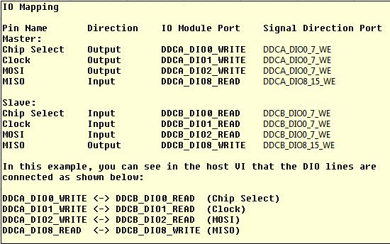
My first question concerns my configuration of the adapter module e/s and selection. I added the IO Module (NI 6581 B: NI 6581 B channel) for my project and selected the channels as shown in the table below. I have a real physical hardware connection as described below using two NI SHC68-C68-D4 cables and a break-out Board.
I changed the names as well:
I selected these DIO channels because I wanted the DDCA connector to be the master and the DDCB connector to be the slave. In addition, in this CLIP every eight channels of i/o has a write enable signal. I have not used the Port configuration because I needed 4 available DIO channels and I saw DIO0-3. Is my logic of selection of channel vs correct Port here?
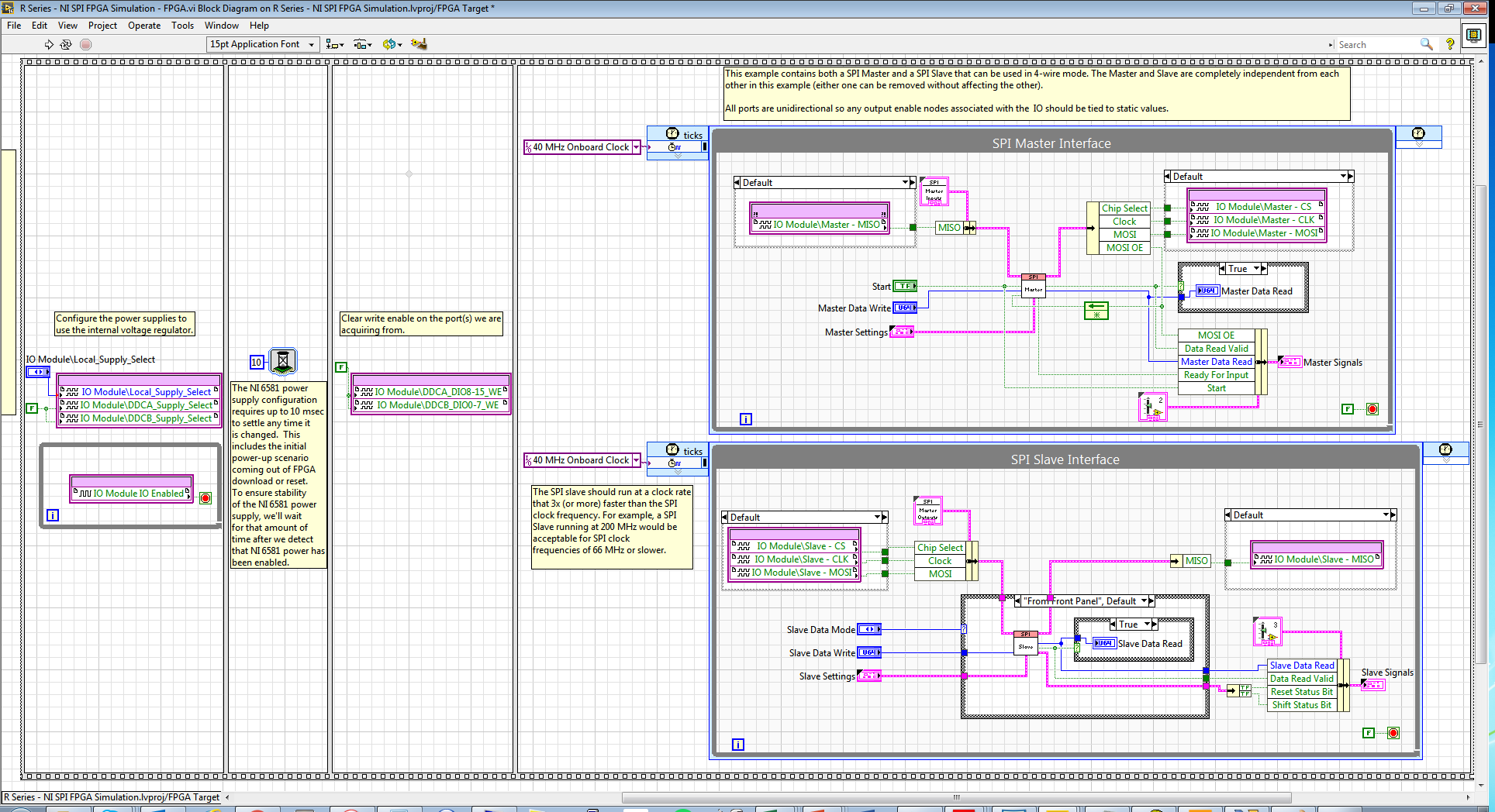
Following the same strategy that examples FlexRIO/NI6581B, I changed the FPGA.vi to include initialization outside of timed loops:
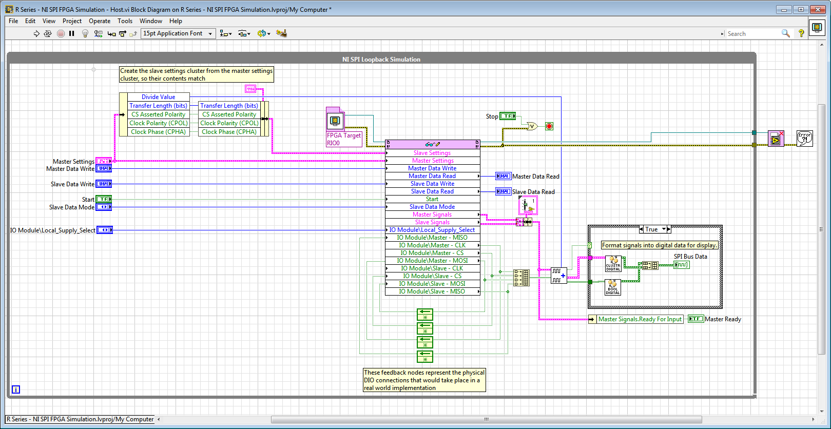
And in the Host.vi I have a node reference FPGA and wired loops of feedback accordingly:
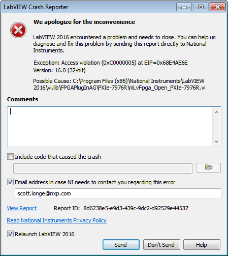
When I compile the FPGA and try to run Host.vi LabVIEW inevitably crashes with Crash Reporter below and must restart:
Does anyone know what I'm doing wrong here? My guess is that it has something to do with the CLIP/IOModule. Any help is appreciated.
Thank you
Scott
Hi Scott,.
I suspect that the problem might be related to the fact that your node open FPGA VI reference is in the while loop and trying to open a new FPGA reference at each iteration.
If you move outside of the while loop, it does not solve the crash?On channel vs port question, your logic seems reasonable to me, but I recommend to try it since this feature could depend on device.
-
I'm looking at the SMU 7857R. I would use the 8 analog inputs and the FPGA to do some annalysisy and DIO based on the best data. I was wondering if it is possible to also define a DAQ task so that all analog data will be made available to the host. Using a data acquisition task would be easier for me to have to write code fpga for use a DMA fifo to send back data.
Hi bcat!
A data acquisition task is only for devices Data Acquisition product supported by driver DAQmx as X-, M-, S-, maps E-Series. The boards of the R series are only supported by the driver OR RIO.
If you don't need pre-treatment on the FPGA so that you can distribute simple data through DMA on your host. If you are looking for an API for the comparable FPGA with the DAQmx API then please check the NI CompactRIO waveform reference library. You can also use the library for R Series boards. -
FPGA/FPGA adapter creates 250 mV voltage offset
I use a high-7971R FPGA in a chassis SMU-1073 with the adaptation Module 5782 (DC coupling) and 2016,08 device drivers. When I turn on the chassis and my computer, nothing strange happens. When I try to run something on the FPGA, however, things get weird. Each piece of code works exactly as it should, but as soon as that 'open FPGA reference' finishes running the adapter begins to produce a voltage mV to 0 to + 250 Ai and AI 1. It doesn't go to AO 0 or 1 AO. This shift of power disappears temporarily as long as 'Reference FPGA open' or "Close FPGA reference" are running, but the only way to get rid of the tension of offset entirely is to restart the chassis. Can someone explain to me why this is happening and how to fix it? The FPGA code, I am running can handle a small shift, but this shift seems to be to saturate the signal.
To see the shift: branch I HAVE 0 and AI 1 directly in a 1 M complete oscilloscope.
It is planned. CDA on this FAM (and more high-end a/d converters) have a range of sampling which is not centered around zero. The front end of the compenstates of the FAM for this by applying an offset from the signal which would appear to the user that the range of the ADC is centered around zero. What is different between this FAMILY and other instruments, is that it is not an additional circuit preventing that this lag observed a user of height of the output of the analog input.
You see the shift happen to reference open FPGA is because that's when power to the GPA is activated. The shift should not have an effect on reading which provides the analog input. Just make sure you have impedance corresponding to the source of the signal at the analogue input and you should be good.
-
Band bandwidth SMU for FPGA chassis
I'm specing on material for an FPGA FlexRIO system. The module FPGA and adapter, we will use has already been defined, a 7975R and a 5782. For our application, we will be streaming 2 inputs analog on a RT controller attached. From my understanding, these samples will be single precision floating point numbers, each of which is a piece of 4 bytes. Assuming that the 5782 max sampling rate is used, 250 MECH. / s, I think that I will need 2 GB/s of bandwidth on my SMU chassis.
Here my question, then, what SMU chassis should I consider? The SMU-1082 has "up to 2 GB/s per-slot dedicated bandwidth", but it is a real or theoretical number? Normally, I would just get the next thing that high, just to be sure, but there is a significant price difference on the way to the SMU 1085, which is also much larger I need. So I would like to save space and several thousands of dollars if I could get away with a 1082. Sampling does not quite to the max modules of adaptation would be acceptable, but I would be interested to know where about my maximum sampling speed would be.
Thanks in advance for your help.
The 1082 has more than enough bandwidth to stream data at a time to the analog inputs of a 5782. The 5782 has a 14 bit ADC with two channels that sample to 250 ms/s. These samples are returned as an I16 with the two least significant bits filled with zeros.
So assuming that you transfer all I16, rather than packing the 14 bits of data, you would have the following bandwidth requirements.
2 channels x 2 bytes/sample x 250 mega-samples per second = 1 GB/s
The 1082 a 2 GB/s of throughput dedicated per slot. The 7975 accommodates up to 1.6 Gbps streaming. I would recommend calling chat with someone, if you are looking for a recommendation on what type of chassis to purchase, but based on the requirements of streaming that you're fine with the combo 7975 and 1082, you thought. Just make sure you get a controller which can accommodate streaming speeds you're looking for. The 8840 is a good candidate.
-
Hello
I would like to smooth out motion of my linear motor. For example, I would like to start a program on the cRIO in scan mode Let's say 1ms interval scan and then perform the interpolation between the points of output (for example, the wave of fishing) on the scan interval 100us. FPGA I wrote programs little but my linear motor does not move. I can't find where I made a mistake or / and something is missing.
Any help would be approciated.
I put in the attachment of my FPGA file, but also the host file I have on the cRIO.
Thank you.
Kamil
Dear Alex,
Thank you interested in my topic. I just understood how do. I went by this example: http://www.ni.com/product-documentation/3598/en/. However I have modyfied somewhat FPGA interpolation method. One described is nove myself smooth enough movement. I have attached files if anyone will need one day. I think that the case is closed.
-
Hello
I use card FPGA 7966R with Module of e/s 6587. I have two sets of screws FPGA, one that uses 6587 mode series (Serdi channel) and the other in parallel mode (Serdi connector). I'm trying to select one of the FPGA VIs via the host VI and I don't know if it's possible.
Some things to note:
- All IOs have the same names, FIFO has the same data type and name.
- Because they use the IO 6587 controller in a different configuration, I can't parallelize them and combine them into a single VI.
Thank you
MILIN
You should take a look at the function of Bitfile dynamic reference opened .
-
Control of read/write of FPGA Interface
I need help on control of FPGA read/write Interface. I would like to connect data TCP Read (String) directly to VI FPGA Read, but the entrance is an FXP... How can I do this?
Then change your FPGA control to be a byte (U8). On the side of your host, use the array of strings of bytes, then Index Array to get the specific byte you want to write on the FPGA.


Maybe you are looking for
-
If I was in a hurry to put up my apple account and don't think through issues of security. I was invited to respond today until I could pay for my products. I gave her too many attempts. Now when I try to pay, it says Apple ID locked. I tried to chan
-
Annoing problem with keyboard focus when redirects to wrong url
When I enter the URL and it wrong, it displays "Page not found" page This time I see already I misspelled and try to correct BUT focus redirects to the "Page not found" page, and I am typing a new URL, nothing helps. To catch the mouse, click the add
-
I tried all of the suggestions posted and have had no success in restarting my print spooler. Help, please. Original title: I tried to restart the print spooler as directed, and he returned the error 2: the system cannot find the specified file. He d
-
Windows 7 will not work a game made for windows XP
Hi, I'm trying to run an old game designed for XP, and it doesn't seem to begin. The game is: Harry Potter Quiditch World Cup. The game installed perfectly, but at startup, it crashes without black screen. After playing with the compatibility mode, w
-
Windows Media Player is the collection of every image in my PC
I had this happens in music and found that they were related to my coolpix camera images and so I removed it. This time there are thousands of images mixed in my videos and my pictures. Some are pictures of games, some are logos of the office as wel